OP-07 Low Offset Low Drift Operational Amplifier
December 1994
OP-07 Low Offset Low Drift Operational Amplifier
General Description
The OP-07 has very low input offset voltage which is obtained by trimming at the wafer stage These low offset voltages generally eliminate any need for external nulling The OP-07 also features low input bias current and high openloop gain The low offsets and high open-loop gain make the OP-07 particularly useful for high-gain applications The wide input voltage range of g 13V minimum combined with high CMRR of 110 dB and high input impedance provide high accuracy in the non-inverting circuit configuration Excellent linearity and gain accuracy can be maintained even at high closed-loop gains Stability of offsets and gain with time or variation in temperature is excellent The OP-07 is available in TO-99 metal can ceramic or molded DIP For improved specifications see the LM607
Features
Y Y Y Y Y Y Y Y
Low VOS 75 mV Max Low VOS Drift 0 6 mV C Max Ultra-Stable vs Time 1 0 mV Month Max Low Noise 0 6 mVp-p Max g 14V Wide Input Voltage Range g 3V to g 18V Wide Supply Voltage Range Fits 725 108A 308A 741 AD510 Sockets Replaces the mA714
Applications
Y Y Y Y
Strain Gauge Amplifiers Thermocouple Amplifiers Precision Reference Buffer Analog Computing Functions
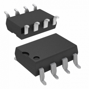
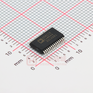
Connection Diagram
Dual-In-Line Package
TL H 10550 – 1
See NS Package Number N08E
Ordering Information
TA e 25 C VOSMax (mV) 75 150 150
Also available per SMD
N08E Plastic OP07EP OP07CP OP07DP
8203602
Operating Temperature Range COM COM COM
C1995 National Semiconductor Corporation
TL H 10550
RRD-B30M115 Printed in U S A
�Absolute Maximum Ratings
If Military Aerospace specified devices are required please contact the National Semiconductor Sales Office Distributors for availability and specifications Supply Voltage Internal Power Dissipation (Note 5) Differential Input Voltage Input Voltage (Note 6) Output Short-Circuit Duration
g 22V
Storage Temperature Range Lead Temperature (Soldering 60 sec ) Junction Temperature
b 65 C to a 150 C
260 C
b 65 C to a 150 C
500 mW g 30V g 22V Continuous
Operating Temperature Range
OP-07E OP-07C OP-07D 0 C to a 70 C
Simplified Schematic
TL H 10550 – 3
R2A and R2B are electronically trimmed on chip at the factory for minimum offset voltage
2
�Electrical Characteristics
Unless otherwise specified VS e g 15V TA e 25 C Boldface type refers to limits over 0 C s TA s 70 C Symbol VOS VOS t IOS IB enp-p en Parameter Input Offset Voltage Long-Term VOS Stability Input Offset Current Input Bias Current Input Noise Voltage Input Noise Voltage Density Input Noise Current Input Noise Current Density Input Resistance Differential-Mode Input Resistance Common-Mode Input Voltage Range Common-Mode Rejection Ratio Power Supply Rejection Ratio Large Signal Voltage Gain VCM e g 13V VS e g 3V to g 18V VS e g 3V to g 18V RL t 2 kX VO e g 10V RL t 2 k X RL t 500X VO e g 0 5V VS e g 3V (Note 4) RL t 10 kX RL t 2 kX RL t 2 k X RL t 1 k X RL t 2 kX (Note 3) AVCL e a 1 (Note 3) VO e 0 IO e 0 VS e g 15V No Load VS e g 3V No Load RP e 20 kX (Note 4) 200 180 150
g 12 5 g 12 0 g 12 0 g 10 5 g 13 0
Conditions Min (Note 1) (Note 2)
OP-07E Typ 30 45 03 05 09
g1 2 g1 5
OP-07C Max 75 130 15 38 53
g4 0 g5 5
Units Max 150 250 20 60 80
g7 0 g9 0
Min
Typ 60 85 04 08 16
g1 8 g2 2
mV mV Mo nA nA mVp-p nV 0Hz pAp-p pA 0Hz
0 1 Hz to 10 Hz (Note 3) fO e 10 Hz fO e 100 Hz (Note 3) fO e 1000 Hz 0 1 Hz to 10 Hz (Note 3) fO e 10 Hz fO e 100 Hz (Note 3) fO e 1000 Hz (Note 4) 15
0 35 10 3 10 0 96 14 0 32 0 14 0 12 50 160
g 14 0
06 18 0 13 0 11 0 30 0 80 0 23 0 17 8
0 38 10 5 10 2 98 15 0 35 0 15 0 13 33 120
g 13 g 14
0 65 20 0 13 5 11 5 35 0 90 0 27 0 18
inp-p in
RIN RINCM IVR CMRR PSRR AVO
MX GX V dB 32 51 mV V
106 103
123 123 5 7 500 450 400
g 13 0 g 12 8 g 12 6 g 12 0
100 97 20 32 120 100 100
g 12 0 g 11 5 g 11 0
120 120 7 10 400 400 400
g 13 0 g 12 8 g 12 6 g 12 0
V mV
VO
Output Voltage Swing
V
SR BW RO Pd
Slew Rate Closed-Loop Bandwidth Output Resistance Power Consumption Offset Adj Range
01 04
03 06 60 75 4
g4
01 04
03 06 60
V ms MHz X 150 8 mW mV 18 mV C
120 6
80 4
g4
TCVOS
TCVOSn TCIOS TCIB
Average Input Offset Voltage Drift Without External Trim With External Trim Average Input Offset Current Drift Average Input Bias Current Drift
03
13
05
RP e 20 kX (Note 4) (Note 3) (Note 3)
03 8 13 3
13 35 35
04 12 18
16 50 50 pA C pA C
�Electrical Characteristics
Unless otherwise specified VS e g 15V TA e 25 C Boldface type refers to limits over 0 C s TA s a 70 C Symbol VOS VOS t IOS IB enp-p en Parameter Input Offset Voltage Long-Term VOS Stability Input Offset Current Input Bias Current Input Noise Voltage Input Noise Voltage Density 0 1 Hz to 10 Hz (Note 3) fO e 10 Hz fO e 100 Hz (Note 3) fO e 1000 Hz 0 1 Hz to 10 Hz (Note 3) fO e 10 Hz fO e 100 Hz (Note 3) fO e 1000 Hz (Note 4) 7 Conditions Min (Note 1) (Note 2) OP-07D Typ 60 85 05 08 16
g2 0 g3 0
Units Max 150 250 30 60 80
g 12 0 g 14 0
mV mV Mo nA nA mVp-p nV 0Hz pAp-p pA 0Hz
0 38 10 5 10 3 98 15 0 35 0 15 0 13 31 120
g 13 g 14
0 65 20 0 13 5 11 5 35 0 90 0 27 0 18
inp-p in
Input Noise Current Input Noise Current Density
RIN RINCM IVR CMRR PSRR AVO
Input Resistance Differential-Mode Input Resistance Common-Mode Input Voltage Range Common-Mode Rejection Ratio Power Supply Rejection Ratio Large Signal Voltage Gain
MX GX V dB 32 51 mV V
VCM e g 13V VS e g 3V to g 18V RL s 2 kX VO e g 10V RL e 2 kX VO e g 10V RL t 500X VO e g 0 5V VS g 3V (Note 4) RL t 10 kX RL t 2 k X RL t 2 k X RL t 1 kX RL t 2 kX (Note 3) AVCL e a 1 (Note 3) VO e 0 IO e 0 VS e g 15V No Load VS e g 3V No Load RP e 20 kX (Note 4)
94 94
110 106 7 10
120 100
400 400 400
V mV
VO
Output Voltage Swing
g 12 0 g 11 5 g 11 0
g 13 0 g 12 8 g 12 6 g 12 0
V
SR BW RO Pd
Slew Rate Closed-Loop Bandwidth Output Resistance Power Consumption Offset Adj Range
01 04
03 06 60 80 4
g4
V ms MHz X 150 8 mW mV 25 mV C
TCVOS
TCVOSn TCIOS TCIB
Average Input Offset Voltage Drift Without External Trim With External Trim Average Input Offset Current Drift Average Input Bias Current Drift
07
RP e 20 kX (Note 4) (Note 3) (Note 3)
07 12 18
25 50 50
mV C pA C pA C
Note 1 VOS is measured approximately 0 5 second after application of power Note 2 Long-Term Offset Voltage Stability refers to the averaged trend line of VOS vs Time over extended periods after the first 30 days of operation Excluding the initial hour of operation changes in VOS during the first 30 operating days are typically 2 5 mV Parameter is sample tested Note 3 Sample Tested Note 4 Guaranteed by design
4
�Test Circuits
Offset Voltage Test Circuit Low Frequency Noise Test Circuit
TL H 10550 – 4 TL H 10550 – 5
Optional Offset Nulling Circuit
TL H 10550 – 6
5
�OP-07 Low Offset Low Drift Operational Amplifier
Physical Dimensions inches (millimeters) (Continued)
Order Number OP-07EP OP-07CP or OP-07DP NS Package Number N08E
LIFE SUPPORT POLICY NATIONAL’S PRODUCTS ARE NOT AUTHORIZED FOR USE AS CRITICAL COMPONENTS IN LIFE SUPPORT DEVICES OR SYSTEMS WITHOUT THE EXPRESS WRITTEN APPROVAL OF THE PRESIDENT OF NATIONAL SEMICONDUCTOR CORPORATION As used herein 1 Life support devices or systems are devices or systems which (a) are intended for surgical implant into the body or (b) support or sustain life and whose failure to perform when properly used in accordance with instructions for use provided in the labeling can be reasonably expected to result in a significant injury to the user
National Semiconductor Corporation 1111 West Bardin Road Arlington TX 76017 Tel 1(800) 272-9959 Fax 1(800) 737-7018
2 A critical component is any component of a life support device or system whose failure to perform can be reasonably expected to cause the failure of the life support device or system or to affect its safety or effectiveness
National Semiconductor Europe Fax (a49) 0-180-530 85 86 Email cnjwge tevm2 nsc com Deutsch Tel (a49) 0-180-530 85 85 English Tel (a49) 0-180-532 78 32 Fran ais Tel (a49) 0-180-532 93 58 Italiano Tel (a49) 0-180-534 16 80
National Semiconductor Hong Kong Ltd 13th Floor Straight Block Ocean Centre 5 Canton Rd Tsimshatsui Kowloon Hong Kong Tel (852) 2737-1600 Fax (852) 2736-9960
National Semiconductor Japan Ltd Tel 81-043-299-2309 Fax 81-043-299-2408
National does not assume any responsibility for use of any circuitry described no circuit patent licenses are implied and National reserves the right at any time without notice to change said circuitry and specifications
�
很抱歉,暂时无法提供与“OP-07CP”相匹配的价格&库存,您可以联系我们找货
免费人工找货- 国内价格
- 1+54.18899
- 10+52.18199
- 100+47.3652
- 500+44.9568
- 国内价格
- 1+31.05
- 10+29.9
- 100+27.14
- 500+25.76
- 国内价格
- 1+31.05002
- 10+29.90002
- 国内价格
- 1+7.6428
- 10+6.4647
- 200+5.0688
- 400+4.4352
- 1000+4.2867
- 国内价格
- 1+4.6233
- 10+3.7719
- 500+2.54876
- 1000+2.42649
- 国内价格
- 1+56.6402
- 10+55.0032
- 100+51.0744
- 500+49.11