2N7002
N−Ch, Enhancement Mode
Field Effect Transistor
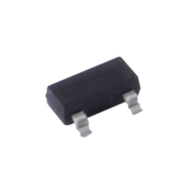
SOT−23 Type Package
Features:
D High Density Cell Design for Low RDS(ON)
D Voltage Controlled Small Signal Switch
D Rugged and Reliable
D High Saturation Current Capability
D
G
S
Absolute Maximum Ratings: (TA = +25C unless otherwise specified)
Drain−Source Voltage, VDSS . . . . . . . . . . . . . . . . . . . . . . . . . . . . . . . . . . . . . . . . . . . . . . . . . . . . . . . . . 60V
Drain−Gate Voltage (RGS 1M), VDGR . . . . . . . . . . . . . . . . . . . . . . . . . . . . . . . . . . . . . . . . . . . . . . 60V
Gate−Source Voltage, VGS
Continuous . . . . . . . . . . . . . . . . . . . . . . . . . . . . . . . . . . . . . . . . . . . . . . . . . . . . . . . . . . . . . . . . . 20V
Non−Repetitive (tp 50s) . . . . . . . . . . . . . . . . . . . . . . . . . . . . . . . . . . . . . . . . . . . . . . . . . . . 40V
Maximum Drain Current, ID
Continuous . . . . . . . . . . . . . . . . . . . . . . . . . . . . . . . . . . . . . . . . . . . . . . . . . . . . . . . . . . . . . . . 115mA
Pulsed . . . . . . . . . . . . . . . . . . . . . . . . . . . . . . . . . . . . . . . . . . . . . . . . . . . . . . . . . . . . . . . . . . . 800mA
Maximum Power Dissipation, PD . . . . . . . . . . . . . . . . . . . . . . . . . . . . . . . . . . . . . . . . . . . . . . . . . 200mW
Derate above 25C . . . . . . . . . . . . . . . . . . . . . . . . . . . . . . . . . . . . . . . . . . . . . . . . . . . . . 1.6mW/C
Operating Junction Temperature Range, TJ . . . . . . . . . . . . . . . . . . . . . . . . . . . . . . . . . . −55 to +150C
Storage Temperature Range, Tstg . . . . . . . . . . . . . . . . . . . . . . . . . . . . . . . . . . . . . . . . . . −55 to +150C
Thermal Resistance, Junction−to−Ambient, Rth(JA) . . . . . . . . . . . . . . . . . . . . . . . . . . . . . . . . . 625C/W
Maximum Lead Temperature (During Soldering, 1/16” from Case, 10sec), TL . . . . . . . . . . . . +300C
Electrical Characteristics: (TA = +25C unless otherwise specified)
Parameter
Symbol
Test Conditions
Min
Typ
Max
Unit
VGS = 0V, ID = 10A
60
−
−
V
VDS = 60V,
VGS = 0
−
−
1.0
A
−
−
0.5
mA
OFF Characteristics
Drain−Source Breakdown Voltage
BVDss
Zero−Gate−Voltage Drain Current
IDSS
TJ = +125C
Gate−Body Leakage Current, Forward
IGSSF
VGSF = 20V, VDS = 0
−
−
100
nA
Gate−Body Leakage Current, Reverse
IGSSR
VGSF = −20V, VDS = 0
−
−
−100
nA
�Electrical Characteristics (Cont’d): (TA = +25C unless otherwise specified)
ON Characteristics (Note 1)
Gate Threshold Voltage
VGS(th)
ID = 250A, VDS = VGS
1.0
2.1
2.5
V
Static Drain−Source ON Resistance
rDS(on)
VGS = 10V,
ID = 500mA
−
1.2
7.5
−
1.7
13.5
−
1.7
7.5
−
2.4
13.5
VGS = 10V, ID = 500mA
−
0.6
3.75
V
VGS = 5V, ID = 50mA
−
0.09
1.5
V
VGS = 5V,
ID = 50mA
Drain−Source ON−Voltage
VDS(on)
ON−State Drain Current
TJ = +100C
TJ = +100C
ID(on)
VGS = 10V, VDS 2 VDS(on)
500
2700
−
mA
gFS
VDS 2 VDS(on), ID = 200mA
80
320
−
mS
Input Capacitance
Ciss
VDS = 25V, VGS = 0V, f = 1MHz
−
20
50
pF
Reverse Transfer Capacitance
Coss
−
11
25
pF
Output Capacitance
Crss
−
4
5
pF
−
−
20
ns
−
−
20
ns
IS
−
−
115
mA
Maximum Pulsed Drain−Source
Diode Forward Current
ISM
−
−
0.8
A
Drain−Source Diode Forward Voltage
VSD
−
0.88
1.5
V
Forward Transconductance
Dynamic Characteristics
Turn−On Time
ton
Turn−Off Time
toff
VDD = 30V, RL = 150,
ID = 200mA, VGS = 10V,
RGEN = 25
Drain−Source Diode Characteristics and Maximum Ratings
Maximum Continuous Drain−Source
Diode Forward Current
VGS = 0V, IS = 115mA, Note 1
Note 1. Pulse Test: Pulse Width 300s, Duty Cycle 2%.
.016 (0.48)
.098
(2.5)
Max
D
G
S
.037 (0.95)
.074 (1.9)
.118 (3.0) Max
.051 (1.3)
.043 (1.1)
.007 (0.2)
�
很抱歉,暂时无法提供与“2N7002”相匹配的价格&库存,您可以联系我们找货
免费人工找货