MPSA92 & MPSA93
Silicon PNP Transistors
High Voltage, General Purpose Amplifier
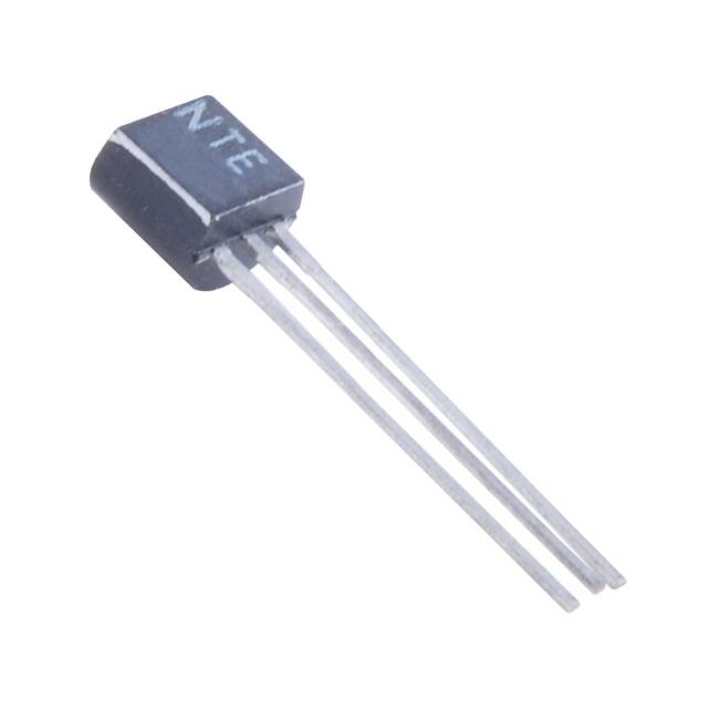
TO−92 Type Package
Absolute Maximum Ratings: (Note 1)
Collector−Emitter Voltage, VCEO
MPSA93 . . . . . . . . . . . . . . . . . . . . . . . . . . . . . . . . . . . . . . . . . . . . . . . . . . . . . . . . . . . . . . . . . . . 200V
MPSA92 . . . . . . . . . . . . . . . . . . . . . . . . . . . . . . . . . . . . . . . . . . . . . . . . . . . . . . . . . . . . . . . . . . . 300V
Collector−Base Voltage, VCBO
MPSA93 . . . . . . . . . . . . . . . . . . . . . . . . . . . . . . . . . . . . . . . . . . . . . . . . . . . . . . . . . . . . . . . . . . . 200V
MPSA92 . . . . . . . . . . . . . . . . . . . . . . . . . . . . . . . . . . . . . . . . . . . . . . . . . . . . . . . . . . . . . . . . . . . 300V
Emitter−Base Voltage, VEBO . . . . . . . . . . . . . . . . . . . . . . . . . . . . . . . . . . . . . . . . . . . . . . . . . . . . . . . . . . 5V
Continuous Collector Current, IC . . . . . . . . . . . . . . . . . . . . . . . . . . . . . . . . . . . . . . . . . . . . . . . . . . 500mA
Total Device Dissipation @ TA = +25C, PD . . . . . . . . . . . . . . . . . . . . . . . . . . . . . . . . . . . . . . . . 625mW
Derate Above +25C . . . . . . . . . . . . . . . . . . . . . . . . . . . . . . . . . . . . . . . . . . . . . . . . . . . . . . 5mW/C
Total Device Dissipation @ TC = +25C, PD . . . . . . . . . . . . . . . . . . . . . . . . . . . . . . . . . . . . . . . . . . . 1.5W
Derate Above +25C . . . . . . . . . . . . . . . . . . . . . . . . . . . . . . . . . . . . . . . . . . . . . . . . . . . . . 12mW/C
Operating Junction Temperature Range, TJ . . . . . . . . . . . . . . . . . . . . . . . . . . . . . . . . . . −55 to +150C
Storage Temperature Range, Tstg . . . . . . . . . . . . . . . . . . . . . . . . . . . . . . . . . . . . . . . . . . −55 to +150C
Thermal Resistance, Junction−to−Ambient, RthJA . . . . . . . . . . . . . . . . . . . . . . . . . . . . . . . . . 200C/mW
Thermal Resistance, Junction−to−Case, RthJC . . . . . . . . . . . . . . . . . . . . . . . . . . . . . . . . . . 83.3C/mW
Note 1. Stresses exceeding Absolute Maximum ratings may damage the device. Absolute Maximum
Ratings are stress ratings only. Functional operation above the Recommended Operating
Conditions is not implied. Extended exposure to stresses above the Recommended Operating
Conditions may affect device reliability.
Electrical Characteristics: (TA = +25C unless otherwise specified)
Parameter
Symbol
Test Conditions
Min
Typ
Max Unit
OFF Characteristics
Collector−Emitter Breakdown Voltage
MPSA92
V(BR)CEO IC = 1mA, IB = 0, Note 2
MPSA93
Collector−Base Breakdown Voltage
MPSA92
300
200
−
−
−
−
V
V
V(BR)CBO IC = 100A, IE = 0
300
200
5
−
−
−
−
−
−
V
V
V
−
−
−
−
−
−
0.25
0.25
0.1
A
A
A
MPSA93
Emitter−Base Breakdown Voltage
Collector Cutoff Current
MPSA92
MPSA93
Emitter Cutoff Current
V(BR)EBO IE = 100A, IC = 0
ICBO
VCB = 200V, IE = 0
IEBO
VCB = 160V, IE = 0
VEB = 3V, IC = 0
Note 2. Pulse Test: Pulse Width 300s, Duty Cycle 2%.
�Electrical Characteristics (Cont’d): (TA = +25C unless otherwise specified)
Parameter
Symbol
Test Conditions
Min
Typ Max Unit
ON Characteristics (Note 2)
DC Current Gain
hFE
IC = 1mA, VCE = 10V
IC = 10mA, VCE = 10V
IC = 30mA, VCE = 10V
25
40
25
−
−
−
−
−
−
IC = 20mA, IB = 2mA
−
−
−
−
−
−
0.5
0.4
0.9
V
V
V
IC = 10mA, VCE = 20V, f = 100MHz
50
−
−
MHz
VCB = 20V, IE = 0, f = 1MHz
−
−
−
−
6
8
pF
pF
Collector−Emitter Saturation Voltage
MPSA92
VCE(sat) IC = 20mA, IB = 2mA
MPSA93
Base−Emitter Saturation Voltage
VBE(sat)
Small−Signal Characteristics
Current Gain − Bandwidth Product
Collector−Base Capacitance
MPSA92
fT
Ccb
MPSA93
Note 1. Pulse Test: Pulse Width 300s, Duty Cycle 2%.
.135 (3.45) Min
.210
(5.33)
Max
Seating Plane
.021 (.445) Dia Max
.500
(12.7)
Min
E B C
.100 (2.54)
.050 (1.27)
.165
(4.2)
Max
.105 (2.67) Max
.205 (5.2) Max
.105 (2.67) Max
�
很抱歉,暂时无法提供与“MPSA93”相匹配的价格&库存,您可以联系我们找货
免费人工找货