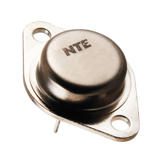
NTE2386
MOSFET
N−Channel Enhancemen Mode,
High Speed Switch
TO3 Type Package
Description:
The NTE2386 Power MOSFET features advantages such as voltage control, very fast switching,
ease of paralleling and temperature stability, and is suited for applications such as switching power
supplies, motor controls, inverters, choppers, audio amplifiers, and high energy pulse circuits.
Features:
� Repetitive Avalanche Ratings
� Dynamic dv/dt Rating
� Simple Drive Requirements
� Ease of Paralleling
D
Case
G
S
Absolute Maximum Ratings:
Continuous Drain Current, ID
(TC = +25�C) . . . . . . . . . . . . . . . . . . . . . . . . . . . . . . . . . . . . . . . . . . . . . . . . . . . . . . . . . . . . . . . 6.2A
(TC = +100�C) . . . . . . . . . . . . . . . . . . . . . . . . . . . . . . . . . . . . . . . . . . . . . . . . . . . . . . . . . . . . . . 2.8A
Pulsed Drain Current (Note 1), IDM . . . . . . . . . . . . . . . . . . . . . . . . . . . . . . . . . . . . . . . . . . . . . . . . . . . 25A
Maximum Power Dissipation (TC = +25�C), PD . . . . . . . . . . . . . . . . . . . . . . . . . . . . . . . . . . . . . . . 125W
(Derate linearly above +25�C) . . . . . . . . . . . . . . . . . . . . . . . . . . . . . . . . . . . . . . . . . . . . . 1.0W/�C
Gate−to−Source Voltage, VGS . . . . . . . . . . . . . . . . . . . . . . . . . . . . . . . . . . . . . . . . . . . . . . . . . . . . . . � 20V
Single Pulse Avalanche Energy (Note 2), EAS . . . . . . . . . . . . . . . . . . . . . . . . . . . . . . . . . . . . . . . 670mJ
Avalanche Current (Repetitive or Non−Repetitive, Note 1), IAR . . . . . . . . . . . . . . . . . . . . . . . . . . 6.2A
Repetitive Avalanche Energy (Note 1), EAR . . . . . . . . . . . . . . . . . . . . . . . . . . . . . . . . . . . . . . . . . . 13mJ
Peak Diode Recovery (Note 3), dv/dt . . . . . . . . . . . . . . . . . . . . . . . . . . . . . . . . . . . . . . . . . . . . . 3.0V/mS
Operating Junction Temperature Range, TJ . . . . . . . . . . . . . . . . . . . . . . . . . . . . . . . . . . −55�to +150�C
Storage Temperature Range, Tstg . . . . . . . . . . . . . . . . . . . . . . . . . . . . . . . . . . . . . . . . . . −55�to +150�C
Lead Temperature (During Soldering, 0.063 in. (1.6mm) from case for 10s), TL . . . . . . . . . . +300�C
Rev. 12−13
�Electrical Characteristics: (TJ = +25�C unless otherwise specified)
Parameter
Symbol
Test Conditions
Min
Typ
Max
Unit
600
−
−
V
Breakdown Voltage
Drain−to−Source
BVDSS
VGS = 0V, ID = 250�A
Static Drain−to−Source
On−State Resistance
RDS(on)
VGS = 10V, ID = 3.4A, Note 4
−
0.97
1.2
�
On−State Drain Current
ID(on)
VDS > ID(on) x RDS(on) Max,
VGS = 10V, Note 4
6.2
−
−
A
Gate Threshold Voltage
VGS(HL)
VDS = VGS, ID = 250�A
2.0
−
4.0
V
VDS = 60V, IDC = 3.4A, Note 4
4.7
70
−
mhos
VDS = Max. Rating VCS = 0V
−
−
250
�A
VDS = 0.8 x Max Rating , VSS = 0V,
TJ = 125�C
−
−
1000
Forward Transconductance
Zero Gate Voltage Drain Current
gs
IDSS
Forward Leakage Current
Gate−to−Source
IGSS
VGS = 20V
−
−
100
nA
Reverse Leakage Current
Gate−to−Source
IGSS
VGS = −20V
−
−
−100
nA
−
4.0
80
nC
−
6.5
8.2
nC
−
20
30
nC
−
1.3
20
ns
−
18
27
−
65
83
−
20
20
Total Gate Charge
Qg
Gate−to−Source Charge
Qgs
Gate−to−Drain (“Miller”) Charge
Qgd
Turn−On Delay Time
td(on)
Rise Time
tr
Turn−Off Delay Time
Fall Time
td(off)
VGS = 10V, ID = 6.2A,
VDS = 0.8 x Max Rating
(independent of operating temperature)
VDD = 300V, fD = 6.2A,
RG = 9.1�� RD = 47�
(independent at operating temperature)
tf
Internal Drain Inductance
LD
Measured from the drain lead, 6mm
(0.25 In) from packaged to center of
die.
−
5.0
−
Internal Source Inductance
LS
Measured from the source lead, 6mm
(0.25 in) from package to source
bonding pad.
−
18
−
VGS = 0V, VDS = 25V, f = 1.0MHz
−
1300
−
nH
Input Capacitance
Ciss
Output Capacitance
Coss
−
150
−
Reverse Transfer Capacitance
Crss
−
30
−
Min
Typ
Max
Unit
−
−
6.2
A
pF
Source−Drain Diode Ratings and Characteristics:
Parameter
Continuous Source Current
(Body Diode)
Symbol
Test Conditions
IS
Pulsed Source Current
(Body Diode)
ISM
Note 1
−
−
26
A
Diode Forward Voltage
VSO
TJ = 25�C, IS = 6.2A, VGS = 0V, Note 4
−
−
1.5
V
Reverse Recovery Time
trr
TJ = 25�C, IF = 6.2A
di/dt = 100A/�s
1.8
3.6
7.9
�C
Forward Turn−On Time
ton
Intrinsic turn−on time is negligible Turn on speed is substantially
controlled by LS + LD
�Thermal Resistance:
Parameter
Symbol
Test Conditions
Min
Typ
Max
Unit
−
−
1.0
�C/W
Junction−to−Case
RthJC
Case−to−Sink
RthCS
Mounting surface flat, smooth, and greased
−
0.12
−
�C/W
Junction−to−Ambient
RthJA
Typical socket mount
−
−
30
�C/W
Note
Note
Note
Note
1.
2.
3.
4.
Repetitive Rating: Pulse Width limited by maximum junction temperature.
VDD = 60V, Starting TJ = 25�C, L = 27mH, RG = 25�, Peak IC = 6.2A
ISD � 6.2A, di/dt = 80A/�s VDD � 3VDSS, TJ � 150�C, Suggested RG = 9.1�
Pulse width � 300�s: Duty Cycle � 2%.
.135 (3.45) Max
.350 (8.89)
.875 (22.2)
Dia Max
Seating
Plane
.312 (7.93) Min
Source
.040 (1.02)
1.187 (30.16)
.665
(16.9)
.215 (5.45)
.156 (3.96) Dia
(2 Holes)
.430
(10.92)
.188 (4.8) R Max
Gate
.525 (13.35) R Max
Drain/Case
�