NTE2394
MOSFET
N−Channel Enhancement Mode,
High Speed Switch
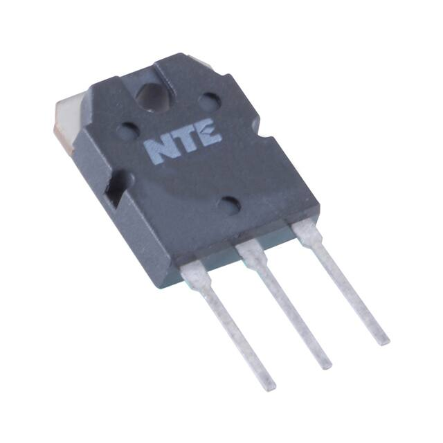
TO3P Type Package
Description:
The NTE2394 is an N−Channel Enhancement Mode Power MOS Field Effect Transistor. Easy drive
and very fast switching times make this device ideal for high speed switching applications. Typical
applications include switching mode power supplies, uninterruptible power supplies, and motor
speed control.
Features:
D High Voltage: 450V for Off−Line SMPS
D High Current: 12A for up to 350W SMPS
D Ultra Fast Switching for Operation at less than 100kHz
Industrial Applications:
D Switching Mode Power Supplies
D Motor Controls
D
G
S
Absolute Maximum Ratings:
Drain−Source Voltage (VGS = 0, Note 1), VDS . . . . . . . . . . . . . . . . . . . . . . . . . . . . . . . . . . . . . . . . . 500V
Drain−Gate Voltage (RGS = 20k�� Note 1), VDGR . . . . . . . . . . . . . . . . . . . . . . . . . . . . . . . . . . . . . . 500V
Gate−Source Voltage, VGS . . . . . . . . . . . . . . . . . . . . . . . . . . . . . . . . . . . . . . . . . . . . . . . . . . . . . . . . . � 20V
Pulsed Drain Current (Note 2), IDM . . . . . . . . . . . . . . . . . . . . . . . . . . . . . . . . . . . . . . . . . . . . . . . . . . . 56A
Clamped Drain Inductive Current (L = 100�H), IDLM . . . . . . . . . . . . . . . . . . . . . . . . . . . . . . . . . . . . . 56A
Continuous Drain Current, ID
TC = +25� C . . . . . . . . . . . . . . . . . . . . . . . . . . . . . . . . . . . . . . . . . . . . . . . . . . . . . . . . . . . . . . . . . . 14A
TC = +100� C . . . . . . . . . . . . . . . . . . . . . . . . . . . . . . . . . . . . . . . . . . . . . . . . . . . . . . . . . . . . . . . . 8.8A
Total Dissipation (TC = +25� C), Ptot . . . . . . . . . . . . . . . . . . . . . . . . . . . . . . . . . . . . . . . . . . . . . . . . . 180W
Derate Above 25� C . . . . . . . . . . . . . . . . . . . . . . . . . . . . . . . . . . . . . . . . . . . . . . . . . . . . . . 1.44W/� C
Maximum Operating Junction Temperature, TJ . . . . . . . . . . . . . . . . . . . . . . . . . . . . . . . . . . . . . . +150� C
Storage Temperature Range, Tstg . . . . . . . . . . . . . . . . . . . . . . . . . . . . . . . . . . . . . . . . . . −55� to +150� C
Note 1. TJ = +25� to +125� C
Note 2. Repetitive Rating: Pulse width limited by maximum junction temperature.
Rev. 10−13
�Thermal Data:
Maximum Thermal Resistance, Junction−to−Case, RthJC . . . . . . . . . . . . . . . . . . . . . . . . . . . 0.69� C/W
Typical Thermal Resistance, Case−to−Sink, RthCS . . . . . . . . . . . . . . . . . . . . . . . . . . . . . . . . . . 0.1� C/W
Maximum Thermal Resistance, Junction−to−Ambient, RthJA . . . . . . . . . . . . . . . . . . . . . . . . . 30� C/W
Maximum Lead Temperature (During Soldering), TL . . . . . . . . . . . . . . . . . . . . . . . . . . . . . . . . . +300� C
Electrical Characteristics: (TC = +25� C unless otherwise specified)
Parameter
Symbol
Test Conditions
Min
Typ
Max
Unit
500
−
−
V
VGS = 0, VDS = Max Rating
−
−
250
�A
VGS = 0, VDS = 400V,
TC = +125� C
−
−
1000
�A
VDS = 0, VGS = � 20V
−
−
� 500
nA
VDS = VGS, ID = 250�A
2
−
4
V
VDS > ID(on) x RDS(on) max,
VGS = 10V
14
−
−
A
VGS = 10V, ID = 7.9A
−
−
0.4
�
9.3
−
−
mho
−
−
3000
pf
−
−
600
pf
−
−
200
pf
−
−
35
ns
−
−
50
ns
td(off)
−
−
150
ns
tf
−
−
70
ns
−
−
120
nC
−
−
14
A
OFF Characteristics
Drain−Source Breakdown Voltage
V(BR)DSS ID = 250�A, VGS = 0
Zero−Gate Voltage Drain Current
Gate−Body Leakage Current
IDSS
IGSS
ON Characteristics (Note 3)
Gate Threshold Voltage
VGS(th)
On−State Drain Current
ID(on)
Static Drain−Source On Resistance
RDS(on)
Dynamic Characteristics
Forward Transconductance
gfs
VDS > ID(on) x RDS(on) max,
ID = 7.9A, Note 4
Input Capacitance
Ciss
Output Capacitance
Coss
VDS = 25V, VGS = 0,
f = 1MHz
Reverse Transfer Capacitance
Crss
Switching Characteristics
Turn−On Time
Rise Time
Turn−Off Delay Time
Fall Time
Total Gate Charge
td(on)
tr
Qg
VDD = 210V, ID = 7.0A,
RI = 4.7�
VGS = 10V, ID = 13A,
VDS = 400V
Source Drain Diode Characteristics
Source−Drain Current
ISD
Source−Drain Current (Pulsed)
ISDM
Note 3
−
−
56
A
Forward ON Voltage
VSD
ISD = 14A, VGS = 0
−
−
1.4
V
IDS = 14A, di/dt = 100A/�s,
TJ = +150� C
−
1300
−
ns
−
7.4
−
�C
Reverse Recovery Time
trr
Reverse Recovered Charge
Qrr
Note 3. Repetitive Rating: Pulse width limited by maximum junction temperature.
Note 4. Pulsed: Pulse Duration = 300�s, Duty Cycle 1.5%
�.190 (4.82)
.615 (15.62)
D
.787
(20.0)
.591
(15.02)
.787
(20.0)
.126
(3.22)
Dia
G
D
S
.215 (5.47)
�
很抱歉,暂时无法提供与“NTE2394”相匹配的价格&库存,您可以联系我们找货
免费人工找货