NTE2631
Integrated Circuit
Quad Differential Line Driver
Functional Description:
The NTE2631 is a quad differential line driver constructed using Advanced Low−Power Schottky
processing in a 16−Lead DIP type package designed for digital data transmission over balanced lines.
This device meets all the requirements of EIA standard RS−422 and federal standard 1020 and is
designed to provide unipolar differential drive to twisted−pair or parallel−wire transmission lines.
The NTE2631 provides an enable and disable function common to all four drivers and features
3−state outputs and logical OR−ed complemtary enable inputs. The inputs are all LS cxompatible
and are all one unit load.
Features:
D 2.0ns Output Skew Typical
D Operation from Single +5V Supply
D Output won’t Load Line when VCC = 0
D Four Line Drivers in One Package for Maximum Package Density
D Output Short−Circuit Protection
D Complementary Outputs
D Meets the Requirements of EIA Standard RS−422
D High Output Drive Capability for 100Ω Terminated Transmission Lines
D Advanced Low−Power Schottky Processing
Absolute Maximum Ratings: (above which the useful life may be impaired)
Supply Voltage . . . . . . . . . . . . . . . . . . . . . . . . . . . . . . . . . . . . . . . . . . . . . . . . . . . . . . . . . . . . . . . . . . . . 7.0V
Input Voltage . . . . . . . . . . . . . . . . . . . . . . . . . . . . . . . . . . . . . . . . . . . . . . . . . . . . . . . . . . . . . . . . . . . . . 7.0V
Output Voltage . . . . . . . . . . . . . . . . . . . . . . . . . . . . . . . . . . . . . . . . . . . . . . . . . . . . . . . . . . . . . . . . . . . . 5.5V
Storage Temperature Range . . . . . . . . . . . . . . . . . . . . . . . . . . . . . . . . . . . . . . . . . . . . −65°C to +165°C
�Electrical Characteristics: (VCC = 5V ±5%, TA = 0° to +70°C, Note 1 unless otherwise specified)
Parameter
Symbol
Test Conditions
Min
Typ
Max
Unit
2.5
3.2
−
V
−
0.32
0.5
V
Output HIGH Voltage
VOH
VCC = Min, IOH = −20mA
Output LOW Voltage
VOL
VCC = Min, IOL = 20mA
Input HIGH Voltage
VIH
VCC = Min
2.0
−
−
V
Input LOW Voltage
VIL
VCC = Max
−
−
0.8
V
Input LOW Current
IIL
VCC = Max, VIN = 0.4V
−
−0.20
−0.36
mA
Input HIGH Current
IIH
VCC = Max, VIN = 2.7V
−
0.5
20
µA
Input Reverse Current
II
VCC = Max, VIN = 7.0V
−
0.001
0.1
mA
Off−State (High Impedance)
Output Current
IO
VCC = Max, VO = 5.5V
−
0.5
20
µA
VO = 0.5V
−
0.5
−20
µA
Input Clamp Voltage
VI
VCC = Min, IIN = 18mA
−
−0.8
−1.5
V
Output Short Circuit Current
ISC
VCC = Max
−30
−60
−150
mA
Power Supply Current
ICC
VCC = Max, all outputs disabled
−
60
80
mA
Input to Output
tPLH
VCC = 5V, TA = +25°C, Load = Note 2
−
12
20
ns
tPHL
−
12
20
ns
Output to Output
SKEW
−
2.0
6.0
ns
Enable to Output
tLZ
−
23
35
ns
−
17
30
ns
−
35
45
ns
−
30
40
ns
VCC =
Max,
VCC = 5V, TA = +25°C, CL = 10pF
tHZ
tZL
VCC = 5V, TA = +25°C, Load = Note 2
tZH
Note 1. All typical values are VCC = 5V, TA = +25°C.
Note 2. CL = 30pF, VIN = 1.3V to VOUT = 1.3V, VPULSE = 0V to +3.0V.
�Pin Connection Diagram
Input A 1
16 VCC
(+) Output A 2
15 Input D
(−) Output A 3
14 (+) Output D
ENABLE 4
13 (−) Output D
(−) Output B 5
12 ENABLE
(+) Output B 6
11 (−) Output C
Input B 7
10 (+) Output C
GND 8
16
9 Input C
9
.260 (6.6) Max
1
8
.785 (19.9) Max
.300 (7.62)
.200 (5.08)
Max
.245
(6.22)
Min
.100 (2.54)
.700 (17.7)
�
很抱歉,暂时无法提供与“NTE2631”相匹配的价格&库存,您可以联系我们找货
免费人工找货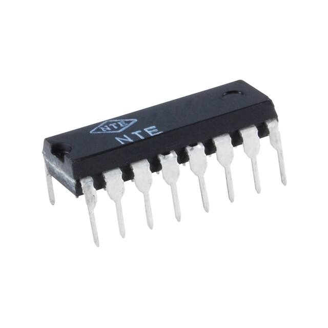


 工商网监
湘ICP备2023018690号
工商网监
湘ICP备2023018690号