NTE2946
MOSFET
N−Channel, Enhancement Mode
High Speed Switch
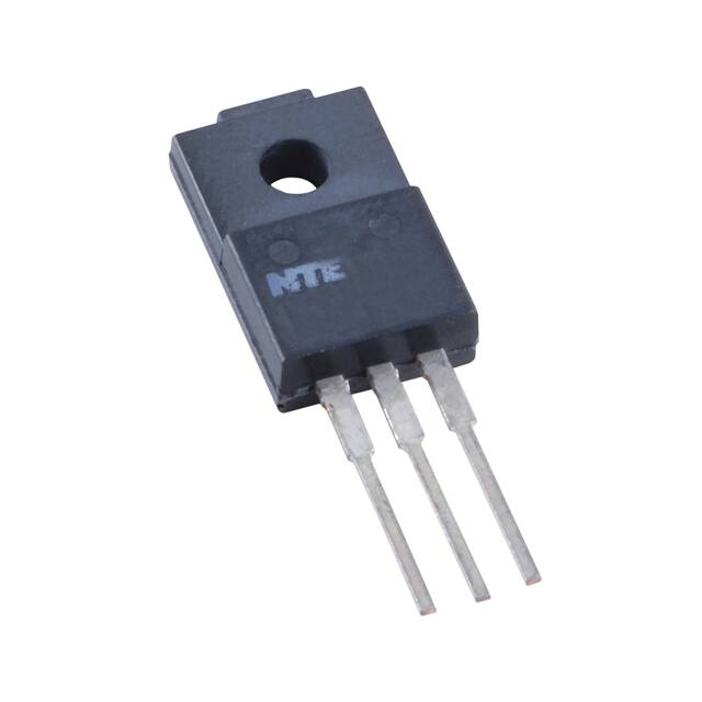
TO220 Full Pack Type Package
Features:
D Low Static Drain−Source ON Resistance
D Improved Inductive Ruggedness
D Fast Switching Times
D Low Input Capacitance
D Extended Safe Operating Area
D Improved High Temperature Reliability
D TO220 Type Isolated Package
D
G
S
Absolute Maximum Ratings:
Drain−Source Voltage (Note 1), VDSS . . . . . . . . . . . . . . . . . . . . . . . . . . . . . . . . . . . . . . . . . . . . . . . . 500V
Drain−Gate Voltage (RGS = 1M+ , Note 1), VDGR . . . . . . . . . . . . . . . . . . . . . . . . . . . . . . . . . . . . . . 500V
Gate−Source Voltage, VGS . . . . . . . . . . . . . . . . . . . . . . . . . . . . . . . . . . . . . . . . . . . . . . . . . . . . . . . . . +20V
Drain Current, ID
Continuous
TC = +255C . . . . . . . . . . . . . . . . . . . . . . . . . . . . . . . . . . . . . . . . . . . . . . . . . . . . . . . . . . . . . . 4.6A
TC = +1005C . . . . . . . . . . . . . . . . . . . . . . . . . . . . . . . . . . . . . . . . . . . . . . . . . . . . . . . . . . . . . 3.2A
Pulsed (Note 2) . . . . . . . . . . . . . . . . . . . . . . . . . . . . . . . . . . . . . . . . . . . . . . . . . . . . . . . . . . . . . . 32A
Gate Current (Pulsed), IGM . . . . . . . . . . . . . . . . . . . . . . . . . . . . . . . . . . . . . . . . . . . . . . . . . . . . . . . . +1.5A
Single Pulsed Avalanche Energy (Note 3), EAS . . . . . . . . . . . . . . . . . . . . . . . . . . . . . . . . . . . . . . 161mJ
Avalanche Current, IAS . . . . . . . . . . . . . . . . . . . . . . . . . . . . . . . . . . . . . . . . . . . . . . . . . . . . . . . . . . . . . 4.6A
Total Power Dissipation (TC = +255C), PD . . . . . . . . . . . . . . . . . . . . . . . . . . . . . . . . . . . . . . . . . . . . 40W
Derate Above 255C . . . . . . . . . . . . . . . . . . . . . . . . . . . . . . . . . . . . . . . . . . . . . . . . . . . . . . 0.32W/5C
Operating Junction Temperature Range, TJ . . . . . . . . . . . . . . . . . . . . . . . . . . . . . . . . . . −555 to +1505C
Storage Temperature Range, Tstg . . . . . . . . . . . . . . . . . . . . . . . . . . . . . . . . . . . . . . . . . . −555 to +1505C
Maximum Lead Temperature (During Soldering, 1/8” from case, 5sec), TL . . . . . . . . . . . . . . +3005C
Thermal Resistance:
Maximum Junction−to−Case, RthJC . . . . . . . . . . . . . . . . . . . . . . . . . . . . . . . . . . . . . . . . . 3.12K/W
Typical Case−to−Sink (Mounting surface flat, smooth, and greased), RthCS . . . . . . . 0.5K/W
Maximum Junction−to−Ambient (Free Air Operation), RthJA . . . . . . . . . . . . . . . . . . . . 62.5K/W
Note 1. TJ = +255 to +1505C.
Note 2. Repetitive Rating: Pulse width limited by maximum junction temperature.
Note 3. L = 14mH, VDD = 50V, RG = 25+ , Starting TJ = +255C.
Rev. 10−13
�Electrical Characteristics: (TC = +255C unless otherwise specified)
Parameter
Symbol
Test Conditions
Min
Typ
Max
Unit
Drain−Source Breakdown Voltage
BVDSS
VGS = 0v, ID = 250.A
500
−
−
V
Gate Threshold Voltage
VGS(th)
VDS = VGS, ID = 250.A
2.0
−
4.0
V
Gate−Source Leakage Forward
IGSS
VGS = 20V
−
−
100
nA
Gate−Source Leakage Reverse
IGSS
VGS = −20V
−
−
−100
nA
Zero Gate Voltage Drain Current
IDSS
VDS = Max. Rating, VGS = 0
−
−
250
.A
VDS = 0.8 Max. Rating, TC = +1255C
−
−
1000
.A
RDS(on)
VGS = 10V, ID = 4A, Note 4
−
−
0.85
+
Forward Transconductance
gfs
VDS . 50V, ID = 4A, Note 4
4.0
6.5
−
mhos
Input Capacitance
Ciss
VGS = 0V, VDS = 25V, f = 1MHz
−
1510
−
pF
Output Capacitance
Coss
−
154
−
pF
Reverse Transfer Capacitance
Crss
−
66
−
pF
Turn−On Delay Time
td(on)
−
14
21
ns
−
23
35
ns
td(off)
−
49
74
ns
tf
−
20
30
ns
−
−
74
nC
−
9
−
nC
−
27
−
nC
(Body Diode)
−
−
8
A
Static Drain−Source ON Resistance
Rise Time
Turn−Off Delay Time
Fall Time
tr
Total Gate Charge
(Gate−Source Plus Gate−Drain)
Qg
Gate−Source Charge
Qgs
Gate−Drain (“Miller”) Charge
Qgd
VDD = 0.5 BVDSS, ID = 8A, ZO = 9.1+ ,
(MOSFET switching times are essentially
independent of operating temperature)
VGS = 10V, ID = 8A, VDS = 0.8 Max.
Rating, (Gate charge is essentially
independent of operating temperature)
Source−Drain Diode Ratings and Characteristics
Continuous Source Current
IS
Pulse Source Current
ISM
(Body Diode) Note 2
−
−
32
A
Diode Forward Voltage
VSD
TJ = +255C, IS = 8A, VGS = 0V, Note 4
−
−
2
V
Reverse Recovery Time
trr
TJ = +255C, IF = 8A, dIF/dt = 100A/.s
−
460
970
ns
Note 2. Repetitive Rating: Pulse width limited by maximum junction temperature.
Note 4. Pulse Test: Pulse Width 3 300.s, Duty Cycle 3 2%.
�.402 (10.2) Max
.224 (5.7) Max
.122 (3.1)
Dia
.295
(7.5)
.165
(4.2)
.669
(17.0)
Max
G
D
S
.531
(13.5)
Min
.100 (2.54)
.059 (1.5) Max
.173 (4.4)
Max
.114 (2.9)
Max
�
很抱歉,暂时无法提供与“NTE2946”相匹配的价格&库存,您可以联系我们找货
免费人工找货- 国内价格
- 1+100.54800
- 200+40.12200
- 500+38.78280
- 1000+38.12400