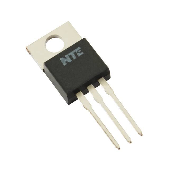
NTE2991
MOSFET
N−Channel, Enhancement Mode
High Speed Switch
TO220 Type Package
Features:
D Ultra Low On−Resistance
D Dynamic dv/dt Rating
D +175C Operating Temperature
D Fast Switching
D Fully Avalanche Rated
D
G
S
Absolute Maximum Ratings:
Drain Current, ID
Continuous (VGS = 10V)
TC = +25C (Note 1) . . . . . . . . . . . . . . . . . . . . . . . . . . . . . . . . . . . . . . . . . . . . . . . . . . . . . . 110A
TC = +100C . . . . . . . . . . . . . . . . . . . . . . . . . . . . . . . . . . . . . . . . . . . . . . . . . . . . . . . . . . . . . . 80A
Pulsed (Note 2) . . . . . . . . . . . . . . . . . . . . . . . . . . . . . . . . . . . . . . . . . . . . . . . . . . . . . . . . . . . . . 390A
Total Power Dissipation (TC = +25C), PD . . . . . . . . . . . . . . . . . . . . . . . . . . . . . . . . . . . . . . . . . . . 200W
Derate Above 25C . . . . . . . . . . . . . . . . . . . . . . . . . . . . . . . . . . . . . . . . . . . . . . . . . . . . . . . 1.3W/C
Gate−Source Voltage, VGS . . . . . . . . . . . . . . . . . . . . . . . . . . . . . . . . . . . . . . . . . . . . . . . . . . . . . . . . . 20V
Single Pulsed Avalanche Energy (IAS = 62A, L = 138H, Note 3), EAS . . . . . . . . . . . . . . . . . . 264mJ
Avalanche Current (Note 2), IAR . . . . . . . . . . . . . . . . . . . . . . . . . . . . . . . . . . . . . . . . . . . . . . . . . . . . . . 62A
Repetitive Avalanche Energy (Note 2), EAR . . . . . . . . . . . . . . . . . . . . . . . . . . . . . . . . . . . . . . . . . . 20mJ
Peak Diode Recovery dv/dt (Note 4), dv/dt . . . . . . . . . . . . . . . . . . . . . . . . . . . . . . . . . . . . . . . . . . 5.0V/ns
Operating Junction Temperature Range, TJ . . . . . . . . . . . . . . . . . . . . . . . . . . . . . . . . . . −55 to +175C
Storage Temperature Range, Tstg . . . . . . . . . . . . . . . . . . . . . . . . . . . . . . . . . . . . . . . . . . −55 to +175C
Maximum Lead Temperature (During Soldering, 1.6mm from case, 10sec), TL . . . . . . . . . . +300C
Maximum Thermal Resistance:
Junction−to−Case, RthJC . . . . . . . . . . . . . . . . . . . . . . . . . . . . . . . . . . . . . . . . . . . . . . . . . 0.75C/W
Junction−to−Ambient, RthJA . . . . . . . . . . . . . . . . . . . . . . . . . . . . . . . . . . . . . . . . . . . . . . . . 62C/W
Typical Thermal Resistance, Case−to−Sink (Flat, greased surface), RthCS . . . . . . . . . . . . 0.50C/W
Note 1. Calculated continuous current based on maximum allowable junction temperature. Package
limitation current is 75A.
Note 2. Repetitive Rating: Pulse width limited by maximum junction temperature.
Note 3. This is a calculated value limited to TJ = +175C.
Note 4. ISD 62A, di/dt 207A/s, VDD V(BR)DSS, TJ +175C.
Rev. 5−19
�Electrical Characteristics: (TJ = +25C unless otherwise specified)
Parameter
Drain−Source Breakdown Voltage
Breakdown Voltage Temperature
Coefficient
Symbol
BVDSS
Test Conditions
VGS = 0V, ID = 250A
V(BR)DSS/ Reference to +25C, ID = 1mA
TJ
Min
Typ
Max
Unit
55
−
−
V
−
0.057
−
V/C
−
−
8.0
m
Static Drain−Source ON Resistance
RDS(on)
VGS = 10V, ID = 62A, Note 5
Gate Threshold Voltage
VGS(th)
VDS = VGS, ID = 250A
2.0
−
4.0
V
VDS = 25V, ID = 62A, Note 5
44
−
−
mhos
VDS = 55V, VGS = 0
−
−
25
A
VDS = 44V, VGS = 0V, TC = +150C
−
−
250
A
Forward Transconductance
Drain−to−Source Leakage Current
gfs
IDSS
Gate−Source Leakage Forward
IGSS
VGS = 20V
−
−
100
nA
Gate−Source Leakage Reverse
IGSS
VGS = −20V
−
−
−100
nA
VGS = 10V, ID = 62A, VDS = 44V
−
−
146
nC
Total Gate Charge
Qg
Gate−Source Charge
Qgs
−
−
35
nC
Gate−Drain (“Miller”) Charge
Qgd
−
−
54
nC
Turn−On Delay Time
td(on)
−
14
−
ns
−
101
−
ns
td(off)
−
50
−
ns
tf
−
65
−
ns
Between lead, 6mm (0.25”) from
package and center of die contact
−
4.5
−
nH
−
7.5
−
nH
VGS = 0V, VDS = 25V, f = 1MHz
−
3247
−
pF
Rise Time
Turn−Off Delay Time
Fall Time
tr
Internal Drain Inductance
LD
Internal Source Inductance
LS
VDD = 28V, ID = 62A, RG = 4.5,
VGS = 10V, Note 5
Input Capacitance
Ciss
Output Capacitance
Coss
−
781
−
pF
Reverse Transfer Capacitance
Crss
−
211
−
pF
(Body Diode)
−
−
110
A
Source−Drain Diode Ratings and Characteristics
Continuous Source Current
IS
Pulse Source Current
ISM
(Body Diode) Note 2
−
−
390
A
Diode Forward Voltage
VSD
TJ = +25C, IS = 62A, VGS = 0V, Note 5
−
−
1.3
V
Reverse Recovery Time
trr
−
69
104
ns
Reverse Recovery Charge
Qrr
TJ = +25C, IF = 62A, di/dt = 100A/s,
Note 5
−
143
215
C
Forward Turn−On Time
ton
Intrinsic turn−on time is neglegible
(turn−on is dominated by LS + LD)
Note 2. Repetitive Rating: Pulse width limited by maximum junction temperature.
Note 5. Pulse Width 400s, Duty Cycle 2%.
�.420 (10.67)
Max
.110 (2.79)
.147 (3.75) Dia Max
.500
(12.7)
Max
.250 (6.35)
Max
.500
(12.7)
Min
.070 (1.78) Max
Gate
.100 (2.54)
Source
Drain/Tab
�