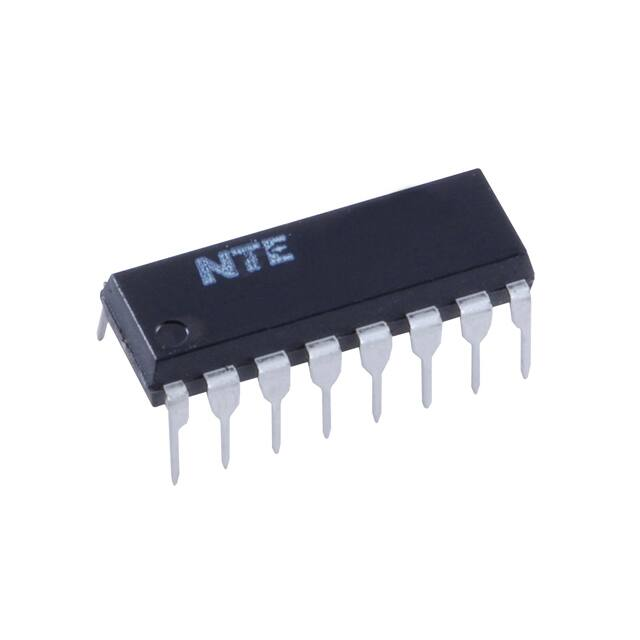
NTE7445
Integrated Circuit
TTL, BCD−toDecimal Decoder/Driver
16−Lead DIP Type Package
Features:
D Full Decoding of Input Logic
D 80mA Sink−Current Capability
D All Outputs are off for Invalid BCD Input Conditions
Description:
The NTE7445 is a monolithic BCD−to−decimal decoder/driver in a 16−Lead DIP type package consisting of eight inverters and ten four−input NAND gates. The inverters are connected in pairs to make
BCD input data available for decoding by the NAND gates. Full decoding of valid BCD input logic
ensures that all outputs remain off for all invalid binary input conditions. This decoder features TTL
inputs and high−performance, NPN output transistors designed for use as an indicator/relay driver
or as an open−collector logic−circuit driver. Each of the high−breakdown output transistors (30 volts)
will sink up to 80 milliamperes of current. Each input is one normalized Series 74 load. Inputs and
outputs are entirely compatible for use with TTL or DTL logic circuits, and the outputs are compatible
for interfacing with most MOS integrated circuits. Power dissipation is typically 215 milliwatts.
Absolute Maximum Ratings: (TA = 0 to +70C unless otherwise specified)
Supply Voltage (Note 1), VCC . . . . . . . . . . . . . . . . . . . . . . . . . . . . . . . . . . . . . . . . . . . . . . . . . . . . . . . . . 7V
Input Voltage, VI . . . . . . . . . . . . . . . . . . . . . . . . . . . . . . . . . . . . . . . . . . . . . . . . . . . . . . . . . . . . . . . . . . 5.5V
Maximum Current Into Any Output (Off−State) . . . . . . . . . . . . . . . . . . . . . . . . . . . . . . . . . . . . . . . . 1mA
Operating Ambient Temperature Range . . . . . . . . . . . . . . . . . . . . . . . . . . . . . . . . . . . . . . . 0C to +70C
Storage Temperature Range . . . . . . . . . . . . . . . . . . . . . . . . . . . . . . . . . . . . . . . . . . . . . −65C to +150C
Note 1. Voltage values are with respect to network GND terminal.
Recommended Operating Conditions:
Parameter
Supply Voltage
Symbol Min
VCC
Off−State Output Voltage
Operating Ambient Temperature
TA
Typ
Max
Unit
4.75
5.0
5.25
V
−
−
30
V
0
−
70
C
�Electrical Characteristics: (TA = 0 to +70C, Note 2 unless otherwise specified)
Parameter
Symbol
Test Conditions
Min Typ Max Unit
High−Level Input Voltage
VIH
2
−
−
V
Low Level Input Voltage
VIL
−
−
0.8
V
Input Clamp Voltage
VIK
−
−
−1.5
V
IO(on) = 80mA
−
0.5
0.9
V
IO(on) = 20mA
−
−
0.4
V
VCC = Min, VIH = 2V, VIL − 800mV,
VO(off) = 30V
−
−
250
A
On−State Output Voltage
VO(on)
Off−State Output Current
IO(off)
VCC = Min, II = −12mA
VCC = Min, VIH = 2V,
VIL = 800mV
Input Current at Max. Input Voltage
II
VCC = Max, VI = 5.5V
−
−
1
mA
High−Level Input Current
IIH
VCC = Max, VI = 2.4V
−
−
40
A
Low−Level Input Current
IIL
VCC = Max, VI = 0.4V
−
−
Supply Current
ICC
VCC = Max, Note 3
−
43
−1.6 mA
70
mA
Note 2. All typical values are at VCC = 5V, TA = +25C. For conditions shown as Min or Max, use the
appropriate value specified under recommended operating conditions for the application
type.
Note 3. ICC is measured with all inputs grounded and outputs open.
Switching Characteristics: (VCC = 5V, TA = +25C unless otherwise specified)
Parameter
Symbol
Propagation Delay Time, Low−to−High Level Output
tPLH
Propagation Delay Time, High−to−Low Level Output
tPHL
Test Conditions
Min Typ Max Unit
CL = 15pF,
RL = 100
−
−
50
ns
−
−
50
ns
Functional Table:
Inputs
Outputs
D
C
B
A
0
1
2
3
4
5
6
7
8
9
0
L
L
L
L
L
H
H
H
H
H
H
H
H
H
1
L
L
L
H
H
L
H
H
H
H
H
H
H
H
2
L
L
H
L
H
H
L
H
H
H
H
H
H
H
3
L
L
H
H
H
H
H
L
H
H
H
H
H
H
4
L
H
L
L
H
H
H
H
L
H
H
H
H
H
5
L
H
L
H
H
H
H
H
H
L
H
H
H
H
6
L
H
H
L
H
H
H
H
H
H
L
H
H
H
7
L
H
H
H
H
H
H
H
H
H
H
L
H
H
8
H
L
L
L
H
H
H
H
H
H
H
H
L
H
9
H
L
L
H
H
H
H
H
H
H
H
H
H
L
H
L
H
L
H
H
H
H
H
H
H
H
H
H
H
L
H
H
H
H
H
H
H
H
H
H
H
H
H
H
L
L
H
H
H
H
H
H
H
H
H
H
H
H
L
H
H
H
H
H
H
H
H
H
H
H
H
H
H
L
H
H
H
H
H
H
H
H
H
H
H
H
H
H
H
H
H
H
H
H
H
H
H
H
INVALID
No.
H = High Level (Off), L = Low Level (On)
�Pin Connection Diagram
Output 0 1
16 VCC
Output 1 2
15 Input A
Output 2 3
14 Input B
Output 3 4
13 Input C
Output 4 5
12 Input D
Output 5 6
11 Output 9
Output 6 7
10 Output 8
GND 8
9 Output 7
16
9
1
8
.260 (6.6)
Max
.870 (22.0) Max
.200
(5.08)
Max
.100 (2.54)
.700 (17.78)
.099 (2.5) Min
�
很抱歉,暂时无法提供与“NTE7445”相匹配的价格&库存,您可以联系我们找货
免费人工找货