NTE74C240 & NTE74C244
Integrated Circuit
TTL− CMOS Octal Buffers and Line Drivers
w/3−State Outputs
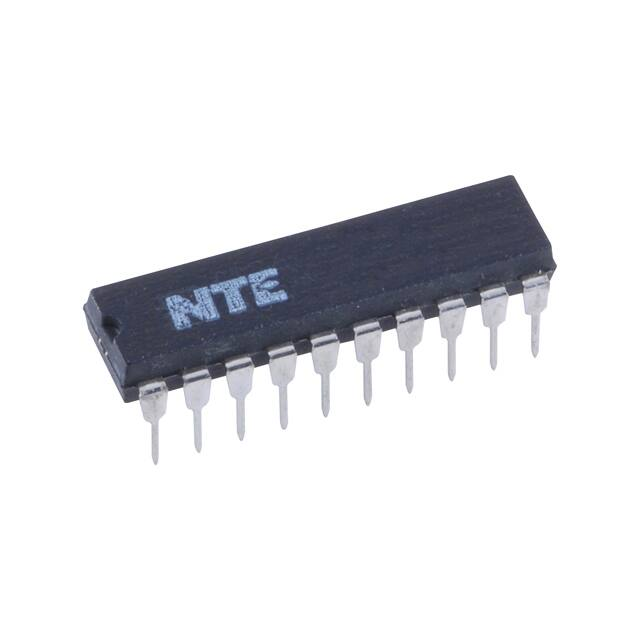
20−Lead DIP
Description:
The NTE74C240 (Inverting) and NTE74C244 (Non−Inverting) octal buffers and line drivers are
monolithic complementary MOS (CMOS) integrated circuits in a 20−Lead DIP type package with
3−state outputs. These outputs have been specially designed to drive highly capacitive loads such
as bus−oriented systems. These devices have a fan out of 6 low power Schottky loads. A high logic
level on the output disable control input G makes the outputs go into the high impedance state.
Features:
D Wide Supply Range: 3V to 15V
D High Noise Immunity: 0.45 VCC (typ)
D Low Power Consumption
D High Capacitive Load Drive Capability
D 3−State Outputs
D Input Protection
D TTL Compatible
D High Speed: 25ns (typ.) at 10V, 50pF (NTE74C244 ONLY)
Absolute Maximum Ratings: (Note 1)
Voltage at Any Pin . . . . . . . . . . . . . . . . . . . . . . . . . . . . . . . . . . . . . . . . . . . . . . . . . . . . −0.3V to VCC +0.3V
Power Dissipation, PD . . . . . . . . . . . . . . . . . . . . . . . . . . . . . . . . . . . . . . . . . . . . . . . . . . . . . . . . . . 700mW
Operating VCC Range . . . . . . . . . . . . . . . . . . . . . . . . . . . . . . . . . . . . . . . . . . . . . . . . . . . . . . . . . . 3V to 15V
Maximum VCC Voltage . . . . . . . . . . . . . . . . . . . . . . . . . . . . . . . . . . . . . . . . . . . . . . . . . . . . . . . . . . . . . . 18V
Operating Temperature Range, TA . . . . . . . . . . . . . . . . . . . . . . . . . . . . . . . . . . . . . . . . . . . −40° to +85°C
Storage Temperature Range, Tstg . . . . . . . . . . . . . . . . . . . . . . . . . . . . . . . . . . . . . . . . . . −65° to +150°C
Lead Temperature (During Soldering, 10sec), TL . . . . . . . . . . . . . . . . . . . . . . . . . . . . . . . . . . . . +260°C
Note 1. “Absolute Maximum Ratings” are those values beyond which th safety of the device cannot
be guaranteed. Except for “Operating Temperature Range”, they are not meant to imply that
the devices should be operated at these limits. The table of “Electrical Characteristics”
provides conditions for actual device operation.
�DC Electrical Characteristics: (TA = −40° to +85°C unless otherwise specified)
Parameter
Symbol
Test Conditions
Min
Typ
Max
Unit
VCC = 5V
3.5
−
−
V
VCC = 10V
8.0
−
−
V
VCC = 5V
−
−
1.5
V
VCC = 10V
−
−
2.0
V
4.5
−
−
V
9.0
−
−
V
−
−
0.5
V
VCC = 10V
−
−
1.0
V
CMOS to CMOS
Logical “1” Input Voltage
Logical “0” Input Voltage
Logical “1” Output Voltage
VIN(1)
VIN(0)
VOUT(1)
VCC = 5V
IO = −10μA
VCC = 10V
Logical “0” Output Voltage
VOUT(0)
VCC = 5V
IO = 10μA
Logical “1” Input Current
IIN(1)
VCC = 15V, VIN = 15V
−
0.005
1.0
μA
Logical “0” Input Current
IIN(0)
VCC = 15V, VIN = 0V
−1.0
−0.005
−
μA
Supply Current
ICC
VCC = 15V
−
0.05
300
μA
CMOS/LPTTL Interface
Logical “1” Input Voltage
VIN(1)
VCC = 4.75V
VCC−1.5
−
−
V
Logical “0” Input Voltage
VIN(0)
VCC = 4.75V
−
−
0.8
V
VOUT(1)
VCC = 4.75V
IO = −450μA
VCC−0.4
−
−
V
IO = −2.2mA
2.4
−
−
V
−
−
0.4
V
VOUT = 0,
TA = +25°C
−14
−30
−
mA
−36
−70
−
mA
VOUT = VCC,
TA = +25°C
12
20
−
mA
48
70
−
mA
Logical “1” Output Voltage
Logical “0” Output Voltage
VOUT(0)
VCC = 4.75V, IO = 2.2mA
Output Drive
Output Source Current (P−Channel)
ISOURCE VCC = 5V
VCC = 10V
Output Sink Current (N−Channel)
ISINK
VCC = 5V
VCC = 10V
AC Electrical Characteristics: (TA = +25°, CL = 50pF, Note 2 unless otherwise specified)
Parameter
Propagation Delay (Data In to Out)
NTE74C240
Symbol
tPD(1), tPD(0)
Test Conditions
Min
Typ
Max
Unit
−
60
90
ns
−
80
110
ns
−
40
70
ns
−
60
90
ns
−
45
70
ns
−
60
90
ns
−
25
50
ns
CL = 150pF
−
40
70
ns
RL = 1kΩ
−
45
80
ns
−
35
60
ns
−
50
90
ns
VCC = 10V
−
30
60
ns
VCC = 5V
−
45
80
ns
−
75
140
ns
−
30
60
ns
−
50
100
ns
VCC = 5V
CL = 150pF
VCC = 10V
CL = 150pF
NTE74C244
VCC = 5V
CL = 150pF
VCC = 10V
Propagation Delay Output Disable to High
Impedance State (from a Logic Level)
t1H, t0H
Propagation Delay Output Disable to Logic
Level (from High Impedance State)
tH1, tH0
Transition Time
VCC = 5V
VCC = 10V
tT(HL), tT(LH)
VCC = 5V
RL = 1kΩ
CL = 150pF
VCC = 10V
CL = 150pF
Note 2. AC Parameters are guaranteed by DC correlated testing.
�AC Electrical Characteristics (Cont’d): (TA = +25°, CL = 50pF, Note 2 unless otherwise specified)
Parameter
Symbol
Test Conditions
Power Dissipation Capacitance
(Output Enabled Buffer)
CPD
Note 4
Power Dissipation Capacitance
(Output Disabled Buffer)
NTE74C240
CPD
Note 4
NTE74C244
Input Capacitance (Any Input)
CIN
Output Capacitance (Output Disabled)
CO
VIN = 0V, f = 1Mhz,
TA = +25°C
Min
Typ
Max
Unit
−
100
−
pF
−
10
−
pF
−
0
−
pF
−
10
−
pF
−
10
−
pF
Note 2. AC Parameters are guaranteed by DC correlated testing.
Note 3. Capacitance is guaranteed by periodic testing.
Note 4. Cpd determines the no load AC power consumption of any CMOS device.
ODA
1
1
0
0
Truth Table (NTE74C240):
IA
OA
ODB
IA
X
X
0
1
Z
Z
1
0
1
1
0
0
X
X
0
1
OB
Z
Z
1
0
1 = High Level
0 = Low Level
X = Don’t Care
Z = 3−State
ODA
1
1
0
0
Truth Table (NTE74C244):
IA
OA
ODB
IA
X
X
0
1
Z
Z
0
1
1
1
0
0
1 = High Level
0 = Low Level
X = Don’t Care
Z = 3−State
Pin Connection Diagram
ODA 1
20 VCC
IA1 2
OB4 3
19 ODB
18 OA1
IA2 4
17 IB4
OB3 5
16 OA2
IA3 6
15 IB3
OB2 7
14 OA3
IA4 8
13 IB2
OB1 9
12 OA4
GND 10
11 IB1
X
X
0
1
OB
Z
Z
0
1
�20
11
1
10
.300 (7.62)
1.200 (30.5) Max
.260 (6.6)
Max
.200
(5.08)
Max
.100 (2.54)
Min
.012
(0.30)
.100 (2.54) Typ
.350 (8.89)
�
很抱歉,暂时无法提供与“NTE74C240”相匹配的价格&库存,您可以联系我们找货
免费人工找货- 国内价格
- 1+128.84400
- 200+51.40800
- 500+49.69080
- 1000+48.84840