NTE911
Integrated Circuit
Dual Voltage Comparator
Description:
The NTE911 is a dual, differential voltage comparator in a 10−Lead Metal Can type package featuring
high accuracy, fast response times, large input voltage range, low power consumption and compatibility with practically all integreated logic forms. When used as a sense amplifier, the threshold voltage
can be adjusted over a wide range, almost independent of the integrated circuit characteristics. Independent strobing of each comparator channel is provided, and pulse stretching on the output is easily
accomplished. Other applications of the dual comparator include a window discriminator in pulse
height detectors and a double−ended limit detector for automatic Go/No−Go test equipment.
Features:
D Fast Response Time − 40ns Typical
D 5mV Maximum Offset Voltage
D 10µA Maximum Offset Current
D Independent Comparator Strobing
Absolute Maximum Ratings:
Positive Supply Voltage . . . . . . . . . . . . . . . . . . . . . . . . . . . . . . . . . . . . . . . . . . . . . . . . . . . . . . . . . . . +14V
Negative Supply Voltage . . . . . . . . . . . . . . . . . . . . . . . . . . . . . . . . . . . . . . . . . . . . . . . . . . . . . . . . . . −7.0V
Peak Output Current . . . . . . . . . . . . . . . . . . . . . . . . . . . . . . . . . . . . . . . . . . . . . . . . . . . . . . . . . . . . . 50mA
Differential Input Voltage . . . . . . . . . . . . . . . . . . . . . . . . . . . . . . . . . . . . . . . . . . . . . . . . . . . . . . . . . ±5.0mA
Input Voltage . . . . . . . . . . . . . . . . . . . . . . . . . . . . . . . . . . . . . . . . . . . . . . . . . . . . . . . . . . . . . . . . . . . . ±7.0V
Strobe Voltage . . . . . . . . . . . . . . . . . . . . . . . . . . . . . . . . . . . . . . . . . . . . . . . . . . . . . . . . . . . . . . 0 to +6.0V
Internal Power Dissipation (TA ≤ +70°C) . . . . . . . . . . . . . . . . . . . . . . . . . . . . . . . . . . . . . . . . . . . . 500mW
Derate Linearly Above +70°C . . . . . . . . . . . . . . . . . . . . . . . . . . . . . . . . . . . . . . . . . . . . 6.3mW/°C
Operating Temperature Range . . . . . . . . . . . . . . . . . . . . . . . . . . . . . . . . . . . . . . . . . . . . . . . 0° to +70°C
Strobe Temperature Range . . . . . . . . . . . . . . . . . . . . . . . . . . . . . . . . . . . . . . . . . . . . . . . −65° to +150°C
Lead Temperature (During Soldering, 10sec) . . . . . . . . . . . . . . . . . . . . . . . . . . . . . . . . . . . . . . . +260°C
Electrical Characteristics: (TA = 25°C, V+ = 12V, V− = −6.0V unless otherwise specified)
Parameter
Input
p Offset Voltage
g
Test Conditions
VOUT = +1.4V,
RS ≤ 200Ω
VCM = 0
RS ≤ 200Ω,
TA = 0° to +70°C
Note 1
VCM = 0
Min
Typ
Max
Unit
−
1.0
5.0
mV
−
1.0
7.5
mV
−
−
6.0
mV
−
−
10
mV
Note 1 The input offset voltage is specified for a logic threshold as follows:
1.5V at 0°C, 1.4 at +25°C, 1.2V at +70°C
�Parameter
Test Conditions
Input
p Offset Current
Min
Typ
Max
Unit
Note 1
VOUT = +1.4V
−
0.5
15
µA
Note 1
TA = 0° to +70°C
−
−
25
µA
−
25
100
µA
−
−
150
µA
700
1500
−
500
−
−
−
40
−
ns
−
12
−
ns
±5
−
−
V
±5
−
−
V
−
200
−
Ω
−
4.5
5.0
V
Input
p Bias Current
TA = 0° to +70°C
Voltage
g Gain
TA = 0° to +70°C
Response Time
Note 2
Strobe Release Time
Input Voltage Range
V = −7V
Differential Input Voltage Range
Output Resistance
Output HIGH Voltage
VIN ≥ 10mV
Loaded Output HIGH Voltage
VIN ≥ 10mV, IO = 5mA
2.5
3.5
−
V
Output LOW Voltage
VIN ≥ 10mV
−1.0
−0.5
0
V
Strobed Output Level
VSTROBE ≤ 0.3V
−1.0
−
0
V
Output Sink Current
VIN ≥ 10mV, VOUT ≥ 0
0.5
0.8
−
mA
Strobe Current
VSTROBE = 100mV
−
1.2
2.5
mA
Positive Supply Current
VOUT = GND, Inverting Input = +10mV
8.6
−
mA
Negative Supply Current
VOUT = GND, Inverting Input = +10mV
−
3.9
−
mA
−
130
230
mW
−
5.0
−
µV/°C
Power Consumption
Temperature Coefficient of Input Offset Voltage
TA = 0° to +70°C
Note 1 The input offset voltage is specified for a logic threshold as follows:
1.5V at 0°C, 1.4 at +25°C, 1.2V at +70°C
Note 2. The response time specified is for a 100mV step input with 5mV overdrive.
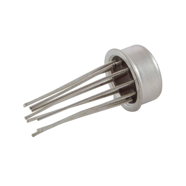
Pin Connection Diagram
(Top View)
Invert Input B
Strobe B
Output
7
6
Non−Invert Input B
5
8
V (−)
4 Non−Invert Input A
9
10
3
V (+)
GND
1
2
Invert Input A
Strobe A
�.335 (8.52) Dia Max
.175
(4.45)
Max
.500
(12.7)
Min
.018 (0.45) Dia Typ
.100 (2.54)
4
3
2
5
6
1
10
.370
(9.4)
Max
7
9
8
.200 (5.08) Dia
�
很抱歉,暂时无法提供与“NTE911”相匹配的价格&库存,您可以联系我们找货
免费人工找货