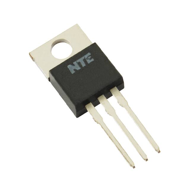
NTE959
Linear Integrated Circuit
Voltage Regulator, Negative, –18V, 1A
Description:
The NTE959 voltage regulator employs current limiting, thermal shutdown, and safe–area compensation which makes it remarkably rugged under most operating conditions. With adequate heat–
sinking they can deliver output currents in excess of 1.0 amperes.
Features:
D No External Components Required
D Internal Thermal Overload Protection
D Internal Short–Circuit Current Limiting
D Output Transistor Safe–Area Compensation
Absolute Maximum Ratings: (TA = +25°C unless otherwise specified)
Input Voltage, VIN . . . . . . . . . . . . . . . . . . . . . . . . . . . . . . . . . . . . . . . . . . . . . . . . . . . . . . . . . . . . . . . . . –35V
Internal Power Dissipation, PD . . . . . . . . . . . . . . . . . . . . . . . . . . . . . . . . . . . . . . . . . . . Internally Limited
Derate Above +25°C . . . . . . . . . . . . . . . . . . . . . . . . . . . . . . . . . . . . . . . . . . . . . . . . . . . 15.4mW/°C
Internal Power Dissipation (TC = +25°C), PD . . . . . . . . . . . . . . . . . . . . . . . . . . . . . . . Internally Limited
Derate Above +75°C . . . . . . . . . . . . . . . . . . . . . . . . . . . . . . . . . . . . . . . . . . . . . . . . . . . . 200mW/°C
Maximum Junction Temperature Range, TJ . . . . . . . . . . . . . . . . . . . . . . . . . . . . . . . . . . –55° to +150°C
Storage Temperature Range, Tstg . . . . . . . . . . . . . . . . . . . . . . . . . . . . . . . . . . . . . . . . . . –65° to +150°C
Thermal Resistance, Junction–to–Ambient, RthJA . . . . . . . . . . . . . . . . . . . . . . . . . . . . . . . . . . . 65°C/W
Thermal Resistance, Junction–to–Case, RthJC . . . . . . . . . . . . . . . . . . . . . . . . . . . . . . . . . . . . . . . 5°C/W
Electrical Characteristics: (VIN = –27V, IO = 500mA, TJ = 0° to +125°C unless otherwise specified)
Parameter
Output Voltage
Line Regulation
Load Regulation
Symbol
VO
RegLine
RegLoad
Test Conditions
Min
Typ
Max
Unit
TJ = +25°C
–17.3 –18.0
–18.7
V
5mA ≤ IO ≤ 1A, PO ≤ 15W,
–33V ≤ VIN ≤ –21V
–17.1 –18.0
–18.9
V
mV
TJ = +25°C,
Note 1
–33V ≤ VIN ≤ –21V
–
25
360
–30V ≤ VIN ≤ –24V
–
10
180
TJ = +25°C,
Note 1
5mA ≤ IO ≤ 1.5A
–
55
360
250mA ≤ IO ≤ 750mA
–
22
180
mV
�Electrical Characteristics: (VIN = –27V, IO = 500mA, TJ = 0° to +125°C unless otherwise specified)
Parameter
Quiescent Current
Quiescent Current Change
Symbol
IB
∆IB
Ripple Rejection
RR
Dropout Voltage
VIN – VO
Test Conditions
Min
Typ
Max
Unit
TJ = +25°C
–
4.5
8.0
mA
–33V ≤ VIN ≤ –21V
–
–
1.0
mA
5mA ≤ IO ≤ 1A
–
–
0.5
32V ≤ VIN ≤ 21V, f = 120Hz
–
57
–
dB
TJ = +25°C, IO = 1A
–
2.0
–
V
Output Noise Voltage
Vn
TA = +25°C, 10Hz ≤ f ≤ 100kHz
–
10
–
µV/VO
Output Resistance
rO
f = 1kHz
–
19
–
mΩ
Short–Circuit Current Limit
Isc
TA = +25°C, VIN = 35V
–
0.2
–
A
TJ = +25°C
–
2.2
–
A
–
–1.1
–
mV/°C
Peak Output Current
Average Temperature
Coefficient of Output
Voltage
Imax
TCVO
Note 1. Load and line regulation are specified at constant junction temperature. Changes in VO
due to heating effects must be taken into account spearately. Pulse testing with low duty
cycle is used.
.420 (10.67)
Max
.110 (2.79)
.147 (3.75)
Dia Max
.500
(12.7)
Max
.250 (6.35)
Max
.500
(12.7)
Min
.070 (1.78)
Max
GND
.100 (2.54)
VOUT
VIN/Tab
�
很抱歉,暂时无法提供与“NTE959”相匹配的价格&库存,您可以联系我们找货
免费人工找货- 国内价格
- 1+23.58720
- 200+9.41760
- 500+9.10440
- 1000+8.94240


 工商网监
湘ICP备2023018690号
工商网监
湘ICP备2023018690号