NTE978

NTE978

  • 厂商:

    NTE

  • 封装:

    DIP14

  • 描述:

    IC-DUAL TIMING CIRCUIT 14-LEAD

  • 详情介绍
  • 数据手册
  • 价格&库存
NTE978 数据手册
NTE978/NTE978C/NTE978SM Integrated Circuit Dual Timer Description: The NTE978 series dual timing circuit is a highly stable controller capable of producing accurate time delays or oscillation. The NTE978 is a dual NTE955. Timing is provided by an external resistor and capacitor for each timing function. The two timers operate independently of each other sharing only VCC and GND. The circuits may be triggered and reset on falling waveforms. The output structures may sink or source 200mA. Features: D Direct Replacement for 556 Timers D Replaces Two 555 Timers (NTE955M) D Timing from Microseconds through Hours D Operates in both Astable and Monostable Modes D Adjustable Duty Cycle D Output can Source or Sink 200mA D Output and Supply TTL Compatible D Temperature Stability better than 0.005% per 5C D Normally On and Normally Off Output D Available in Three Types: NTE978 14−Lead DIP NTE978C 14−Lead DIP (CMOS) NTE978SM SOIC−14 (Surface Mount) Applications: D Precision Timing D Pulse Generation D Sequential Timing D Time Delay Generation D Pulse Width Modulation D Pulse Position Modulation D Linear Ramp Generator Absolute Maximum Ratings: Supply Voltage, VCC . . . . . . . . . . . . . . . . . . . . . . . . . . . . . . . . . . . . . . . . . . . . . . . . . . . . . . . . . . . . . . . +18V Power Dissipation (Note 1), PD . . . . . . . . . . . . . . . . . . . . . . . . . . . . . . . . . . . . . . . . . . . . . . . . . . 1620mW Operating Temperature Range, TA . . . . . . . . . . . . . . . . . . . . . . . . . . . . . . . . . . . . . . . . . . . . . 05 to +705C Storage Temperature Range, Tstg . . . . . . . . . . . . . . . . . . . . . . . . . . . . . . . . . . . . . . . . . . −655 to +1505C Lead Temperature (During Soldering, 10sec Max), TL . . . . . . . . . . . . . . . . . . . . . . . . . . . . . . . . +2605C Note 1. For operating at elevated temperatures the device must be derated based on a +1505C maximum junction temperature and a thermal resistance of +775C/W for NTE978 and NTE978C and +1105C/W for NTE978SM. Rev. 6−14 Electrical Characteristics: (TA = +255C, VCC = +5V to +15V, unless otherwise specified) Parameter Symbol Supply Voltage VCC Supply Current (Each Timer Section) ICC Test Conditions Min Typ Max Unit 4.5 − 16 V VCC = 5V, RL = 8 − 3 6 mA VCC = 15V, RL = 8 − 10 14 mA − 0.75 − % − 50 − ppm/5C − 1.5 − % − 0.1 − %/V − 2.25 − % − 150 − ppm/5C − 3.0 − % − 0.30 − %/V VCC = 15V 4.5 5.0 5.5 V VCC = 5V 1.25 1.67 2.0 V − 0.2 1.0 5A 0.4 0.5 1.0 V − 0.1 0.6 mA VTH = V−Control, Note 5 − 0.03 0.1 5A VTH = 11.2V − − 250 nA VCC = 15V 9 10 11 V VCC = 5V 2.6 3.33 4.0 V − 1 100 nA VCC = 15V, I = 15mA − 180 300 mV VCC = 4.5V, I = 4.5mA − 80 200 mV ISINK = 10mA − 0.1 0.25 V ISINK = 50mA − 0.4 0.75 V ISINK = 100mA − 2.0 2.75 V ISINK = 200mA − 2.5 − V VCC = 5V ISINK = 5mA − 0.25 0.35 V VCC = 15V ISOURCE = 200mA − 12.5 − V ISOURCE = 100mA 12.75 13.3 − V 2.75 3.3 − V Low State, Note 2 Timing Error, Monostable Initial Accuracy RA = 1k to 100k+ , C = 0.15 F, Note 3 Drift with Temperature Accuracy over Temperature Drift with Supply Timing Error, Astable Initial Accuracy RA, RB = 1k to 100k+ , C = 0.15 F, Note 3 Drift with Temperature Accuracy over Temperature Drift with Supply Trigger Voltage VT Trigger Current IT Reset Voltage VR Reset Current IR Threshold Current ITH Control Voltage Level and Threshold Voltage VCL VTH Pin1, Pin13 Leakage Output High Idis Pin1, Pin13 Saturation Output Low Output Voltage Drop (Low) Output Voltage Drop (High) Note 4 Note 6 VOL VOH VCC = 15V VCC = 5V Rise Time of Output tOLH − 100 − ns Fall Time of Output tOHL − 100 − ns − 0.1 2.0 % − +10 − ppm/5C − 0.2 0.5 %/V Matching Characteristics Initial Timing Accuracy Timing Druft with Temperature Drift with Supply Voltage Note 7 Note Note Note Note 2. 3. 4. 5. Supply current when output high typically 1mA less at VCC = 5V. Tested at VCC = 5V and VCC = 15V. As reset voltage lowers, timing is inhibited and then the output goes low. This will determine the maximum value of RA + RB for 15V operation. The maximum total (RA + RB) is 20M+ . Note 6. No protection against excessive Pin1, Pin13 current is necessary providing the package dissipation rating will not be exceeded. Note 7. Matching characteristics refer to, the difference between performance characteristics of each timer section. NTE978, NTE978C Pin Connection Diagram Discharge 1 14 VCC Threshold 2 13 Discharge Control Voltage 3 12 Threshold Reset 4 14 8 1 7 11 Control Voltage Output 5 10 Reset Trigger 6 9 Output GND 7 8 Trigger .785 (19.95) Max .300 (7.62) .200 (5.08) Max .100 (2.45) .099 (2.5) Min .600 (15.24) NTE978SM .340 (8.64) 14 8 1 7 .236 (5.99) .154 (3.91) .050 (1.27) 016 (.406) .198 (5.03) 061 (1.53) .006 (.152) NOTE: Pin1 on Beveled Edge
NTE978
物料型号:NTE978/NTE978C/NTE978SM

器件简介: NTE978系列双定时电路是一种高稳定性控制器,能够产生精确的时间延迟或振荡。该系列是双NTE955定时器,通过外部电阻和电容为每个定时功能提供计时。两个定时器独立操作,仅共享VCC和GND。电路可以在下降波形上触发和复位。输出结构可以吸收或提供200mA电流。

引脚分配: - 
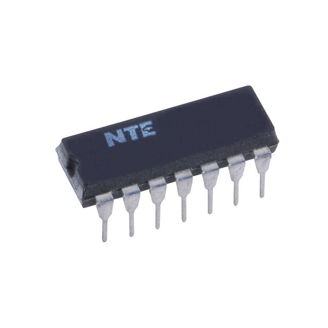
NTE978和NTE978C有14个引脚,其中1号引脚为输出,6号和8号引脚为触发输入,11号和13号引脚为控制电压/阈值引脚,14号引脚为GND。 - NTE978SM为表面贴装版本,引脚配置与NTE978和NTE978C相似,但形状不同。

参数特性: - 供电电压范围:+18V - 功耗:1620mW - 工作温度范围:0到+70°C - 存储温度范围:-65到+150°C - 引脚耐温:+260°C(焊接时,最多10秒)

功能详解: - 直接替代556定时器 - 可替换两个555定时器(NTE955M) - 计时范围从微秒到小时 - 可操作在稳定和单稳态模式 - 可调占空比 - 输出与TTL兼容 - 温度稳定性优于0.005%每摄氏度

应用信息: - 精密计时 - 脉冲生成 - 顺序计时 - 时间延迟生成 - 脉冲宽度调制 - 脉冲位置调制 - 线性斜坡发生器

封装信息: - NTE978:14脚DIP封装 - NTE978C:14脚DIP封装(CMOS) - NTE978SM:SOIC-14表面贴装封装
NTE978 价格&库存

很抱歉,暂时无法提供与“NTE978”相匹配的价格&库存,您可以联系我们找货

免费人工找货