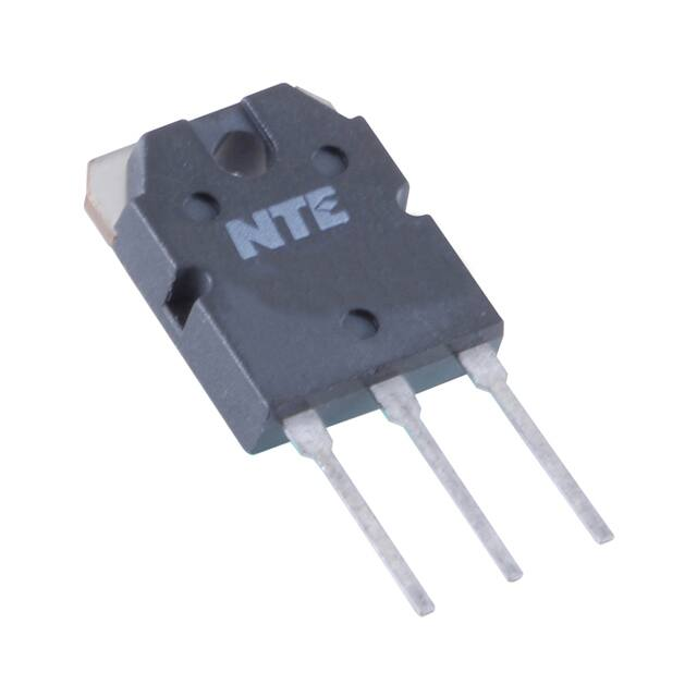
TIP142
Silicon NPN Transistor
Darlington Power Amp, Switch
TO−247 Type Package
Description:
The TIP142 is a silicon NPN Darlington transistor in a TO−247 type package designed for general
purpose amplifier and low frequency switching applications.
Features:
D High DC Current Gain: hFE = 1000 (Min) at IC = 5A, VCE = 4V
D Collector−Emitter Sustaining Voltage: VCEO(sus) = 100V (Min) at IC = 30mA
Absolute Maximum Ratings: (Note 1)
Collector−Emitter Voltage, VCEO . . . . . . . . . . . . . . . . . . . . . . . . . . . . . . . . . . . . . . . . . . . . . . . . . . . . . 100V
Collector−Base Voltage, VCB . . . . . . . . . . . . . . . . . . . . . . . . . . . . . . . . . . . . . . . . . . . . . . . . . . . . . . . . 100V
Emitter−Base Voltage, VEB . . . . . . . . . . . . . . . . . . . . . . . . . . . . . . . . . . . . . . . . . . . . . . . . . . . . . . . . . . . 5V
Collector Current, IC
Continuous . . . . . . . . . . . . . . . . . . . . . . . . . . . . . . . . . . . . . . . . . . . . . . . . . . . . . . . . . . . . . . . . . . 10A
Peak (Note 2) . . . . . . . . . . . . . . . . . . . . . . . . . . . . . . . . . . . . . . . . . . . . . . . . . . . . . . . . . . . . . . . . 15A
Base Current, IB . . . . . . . . . . . . . . . . . . . . . . . . . . . . . . . . . . . . . . . . . . . . . . . . . . . . . . . . . . . . . . . . 500mA
Total Power Dissipation (TC = +25C), PD . . . . . . . . . . . . . . . . . . . . . . . . . . . . . . . . . . . . . . . . . . . 125W
Operating Junction Temperature Range, TJ . . . . . . . . . . . . . . . . . . . . . . . . . . . . . . . . . . −65 to +150C
Storage Temperature Range, Tstg . . . . . . . . . . . . . . . . . . . . . . . . . . . . . . . . . . . . . . . . . . −65 to +150C
Thermal Resistance, Junction−to−Case, RthJC . . . . . . . . . . . . . . . . . . . . . . . . . . . . . . . . . . . . . 1.0C/W
Thermal Resistance, Junction−to−Ambient, RthJA . . . . . . . . . . . . . . . . . . . . . . . . . . . . . . . . . . 35.7C/W
Note 1. Stresses exceeding those listed in the Absolute Maximum Ratings table may damage the
device. If any of these limits are exceeded, device functionality should not be assumed, damages may occur and reliability may be affected.
Note 2. 5ms, 10% Duty Cycle
Electrical Characteristics: (TC = +25C unless otherwise specified)
Parameter
Symbol
Test Conditions
Min
Typ
Max
Unit
VCEO(sus) IC = 30mA, IB = 0, Note 3
100
−
−
V
OFF Characteristics
Collector−Emitter Sustaining Voltage
Collector Cutoff Current
Emitter Cutoff Current
ICBO
VCB = 100V, IE = 0
−
−
1.0
mA
ICEO
VCE = 50V, IB = 0
−
−
2.0
mA
IEBO
VBE = 5V
−
−
2
mA
Note 3. Pulse Test: Pulse Width = 300s, Duty Cycle 2%.
�Electrical Characteristics (Cont’d): (TC = +25C unless otherwise specified)
Parameter
Symbol
Test Conditions
Min
Typ
Max
Unit
VCE = 4V, IC = 5A
1000
−
−
VCE = 4V, IC = 10A
500
−
−
IC = 5A, IB = 10mA
−
−
2.0
V
IC = 10A, IB = 40mA
−
−
3.0
V
ON Characteristics (Note 3)
DC Current Gain
hFE
Collector−Emitter Saturation Voltage
VCE(sat)
Base−Emitter Saturation Voltage
VBE(sat)
IC = 10A, IB = 40mA
−
−
3.5
V
Base−Emitter On Voltage
VBE(on)
IC = 10A, VCE = 4V
−
−
3.0
V
VCC = 30V, IC = 5A, IB = 20mA,
Duty Cycle 2%, IB1 = IB2,
RC & RB Varied, TJ = +25C
−
0.15
−
s
−
0.55
−
s
−
2.5
−
s
−
2.5
−
s
Switching Characteristics
Delay Time
td
Rise Time
tr
Storage Time
ts
Fall Time
tf
Note 3. Pulse Test: Pulse Width = 300s, Duty Cycle 2%.
.626 (15.9)
Max
.197 (5.0)
.217
(5.5)
.787
(20.0)
.143 (3.65)
Dia Max
B
C
B
C
E
.157
(4.0)
.559
(14.2)
Min
E
.215 (5.45)
.047 (1.2)
.094 (2.4)
�
很抱歉,暂时无法提供与“TIP142”相匹配的价格&库存,您可以联系我们找货
免费人工找货