Freescale Semiconductor
User’s Guide
Document Number: MC13192RFCUG
Rev. 1.2, 09/2006
MC13192 RF Daughter Card
User’s Guide
1
Introduction
The MC13192 RF Daughter Card (13192RFC-A00) is used in conjunction with a microcontroller
development board for RFIC evaluation, code development, and system evaluation. It interfaces directly
to the M68EVB908GB60 HCS08 family Microcontroller Development Board but it can be adapted to
other boards that offer access to the MCU input/output ports.
The RF Daughter Card is configured with all the off-chip circuitry required for functional performance of
the MC13192 RF data modem except the MCU. The MCU interface required by the RFIC is pinned out at
the edge of the card using standard header pins. The RF interface is accomplished through SMA
connectors for the TX and RX ports. The SMA connectors can be connected to test equipment using coax
cables for testing or connected to screw-on antennas (two provided) for testing purposes.
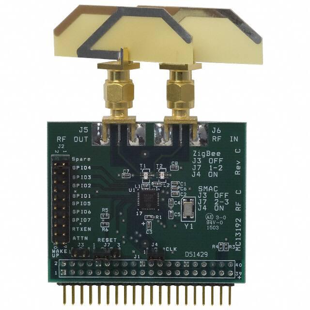
Figure 1-1 shows the RF Daughter Card with the two detachable dipole antennas.
Figure 1-1. MC13192 RF Daughter Card with Antennas
© Freescale Semiconductor, Inc., 2004, 2005, 2006. All rights reserved.
�MCU Interface
Figure 1-2 shows the RF Daughter Card installed in a GB60 development board.
Figure 1-2. RF Daughter Card Installed in the GB60 Development Board
2
MCU Interface
Refer to the MC13192 Data Sheet and/or MC13192 Reference Manual for interface details.
MC13192 RF Daughter Card, Rev. 1.2
2
Freescale Semiconductor
�Safety Information
3
Safety Information
Any modifications to this product may violate the rules of the Federal Communications Commission and
make operation of the product unlawful.
47 C.F.R. Sec. 15.21
This equipment has been tested and found to comply with the limits for a Class B digital device, pursuant
to part 15 of the FCC Rules. These limits are designed to provide reasonable protection against harmful
interference in a residential installation. This equipment generates uses and can radiate radio frequency
energy and, if not installed and used in accordance with the instructions, may cause harmful interference
to radio communications. However, there is no guarantee that interference will not occur in a particular
installation. If this equipment does cause harmful interference to radio or television reception, which can
be determined by turning the equipment off and on, the user is encouraged to try to correct the interference
by one or more of the following measures:
• Reorient or relocate the receiving antenna.
• Increase the separation between the equipment and receiver.
• Connect the equipment into an outlet on a circuit different from that to which the receiver is
connected.
• Consult the dealer or an experienced radio/TV technician for help.
47 C.F.R. Sec.15.105(b)
This equipment complies with FCC radiation exposure limits set forth for an uncontrolled environment.
The antenna(s) used for this equipment must be installed to provide a separation distance of at least 8
inches (20cm) from all persons.
This device complies with Part 15 of the FCC Rules. Operation is subject to the following two conditions:
• This device may not cause harmful interference.
• This device must accept any interference received, including interference that may cause undesired
operation.
MC13192 RF Daughter Card, Rev. 1.2
Freescale Semiconductor
3
�Daughter Card Description
4
Daughter Card Description
Figure 4-1 shows the top side and component layout of the RF Daughter Card PCB.
Figure 4-1. RF Daughter Card PCB (Top View)
Figure 4-2 shows the bottom side of the RF Daughter Card PCB.
Figure 4-2. RF Daughter Card PCB (Bottom View)
As shown in Figure 1-2 and Figure 4-1 , connector J1 is the main interface to the GB60 Development
Board. The interface connections described in Section 4.2, “Connections”, fall under the following three
broad categories:
1. Serial Peripheral Interface (SPI)
2. Control
3. Power
MC13192 RF Daughter Card, Rev. 1.2
4
Freescale Semiconductor
�Daughter Card Description
4.1
SPI Connections
J1 Pins 35 through 38 provide the following four wire SPI interface:
• MOSI
• SPICLK
• CE
• MISO
The MC13192 always functions as a slave device. SPI operation is described in detail in the MC13192
Data Sheet and/or MC13192 Reference Manual.
4.2
Connections
The following sections describe the interconnects for the GB60 Development Board.
4.2.1
•
•
•
Control Connections
J1 Pin 19 is the IRQ line from MC13192. Connection to the MCU depends on how the MCU
services interrupts.
J1 Pin 31, RXTXEN, allows the MCU to initiate transceiver functions.
J1 Pin 34, the ATTN line, allows the MCU to wake up the MC13192 from Doze or Hibernate low
power modes.
NOTE
RXTXEN and ATTN are also available at header J2 for manual control.
•
•
•
•
•
•
4.2.2
J1 Pin 24 provides the MC13192 CLKO to the MCU when a jumper is installed at J4.
J1 Pin 32 interfaces with the MCU to provide a Reset to the MC13192 and header J7 controls the
functionality.
When Pin 2 and Pin 3 of J7 are shunted, the MC13192 and the MCU can be reset simultaneously.
When Pin 1 and Pin 2 of J7 are shorted, the MCU will reset the MC13192.
Pin 5 and Pin 22 of J1 provide a wake up function to the MCU when a shunt is installed at J3.
Pin 13 and Pin 14 of J1 provide access to MC13192 GPIO1 and GPIO2 ports.
Power Connections
J1 Pin 39 provides the supply voltage to the RF Daughter Card. Voltage on this line should not exceed
3.6 VDC and the nominal supply should not exceed 3.4 VDC. J1 Pin 40 is ground.
4.2.3
Non-MCU connections
Header J2 provides connections to a number of MC13192 contacts for non-MCU connections. As already
stated, the RXTXEN and ATTN lines are available at J2 for external control using switches or other
hardware. The MC13192 GPIO are also available for interface to external hardware.
MC13192 RF Daughter Card, Rev. 1.2
Freescale Semiconductor
5
�Software Configuration
5
Software Configuration
As shown in Figure 4-1, the legend printed on the RF Daughter Card PCB shows the jumper settings for
ZigBee and SMAC applications. The SMAC jumper settings on the board can now be ignored because as
of this release, the SMAC and 802.15.4 MAC use the same settings.
6
Bill of Materials and Schematic
Table 6-1 shows the RF Daughter Card bill of materials (BOM).
Table 6-1. Bill of Materials
Item
Quantity
Reference
Part
1
3
C1,C2,C3,C8
100pF /0402
2
2
C4,C5
9pF /0402
3
2
C7,C6
1nF /0402
5
1
J1
MCU Interface Header 20X2
6
1
J2
Interface HEADER 10X2
7
1
J3
Wake Up Header 1X2
8
1
J4
CLK SOURCE Header 1X2
9
2
J6,J5
Connector SMA
10
1
L1
8.2nH /0402
11
1
L2
6.8nH /0402
12
1
R1,R4,R5,R6
47kΩ /0402
13
1
R2
200Ω /0402
14
1
R3
10kΩ /0402
15
2
T1,T2
16
1
16
1
Part Number
Source
142-0701-881
Johnson
Balun Transformer
2450BL15B200
Johnson
U1
IC
MC13192
Freescale
Semiconductor
Y1
Crystal
TSX-10A@16MHz
Toyocom
Figure 6-1 shows the RF Daughter Card schematic.
MC13192 RF Daughter Card, Rev. 1.2
6
Freescale Semiconductor
�1
L1
T1
2450BL15B100
R2
L2
C8
100 pF
3.9 nH
2
SMA
2
200 Ω
6.8 nH
2
J6
C7
1 nF
5
4
1
3
1
1
3
5
4
2
T2
2450BL15B100
C1
100 pF
C2
100 pF
C4
9 pF
RFINRFIN+
GND
GND
PAO+
PAOGND
GPIO4
MC13192
1
2
3
4
5
6
7
8
U1
2
SMA
Y1
TSX-10A@16MHz
1
3
5
7
9
11
13
4
6
8
10
12
14
J5
32
31
30
29
28
27
26
25
VDDA
VBATT
VDDVCO
VDDLO1
VDDLO2
XTAL2
XTAL1
GPIO7
GPIO6
GPIO5
VDDINT
VDDD
IRQ
CE
MISO
MOSI
J2
HEADER 10X2
GPIO3
GPIO2
GPIO1
RST
RXTXEN
ATTN
CLKO
SPICLK
9
10
11
12
13
14
15
16
15
17
19
MC13192 RF Daughter Card, Rev. 1.2
16
18
20
MOTOROLA
18
17
24
23
22
21
20
19
C5
9 pF
RTXEN
GPIO1
GPIO2
C3
100 pF
C6
1 nF
R4
47 kΩ
R3
10 kΩ
RTXEN
MOSI
CE
VCC
IRQ
GPIO1
R1
47 kΩ
PA2
1
3
5
7
9
11
13
15
17
19
21
23
25
27
29
31
33
35
37
39
MCU Interface
J1
2
4
6
8
10
12
14
16
18
20
22
24
26
28
30
32
34
36
38
40
R6
47 kΩ
RST
SPICLK
MISO
MCU RESET
ATTN
RXD
CLKO from MC13192
GPIO2
R5
47 kΩ
3
2
1
2
1
1
2
RESET
J7
CLK Source
J4
Wake Up
J3
NOTES
Figure 6-1. RF Daughter Card Schematic
7
�How to Reach Us:
Home Page:
www.freescale.com
E-mail:
support@freescale.com
USA/Europe or Locations Not Listed:
Freescale Semiconductor
Technical Information Center, CH370
1300 N. Alma School Road
Chandler, Arizona 85224
+1-800-521-6274 or +1-480-768-2130
support@freescale.com
Europe, Middle East, and Africa:
Freescale Halbleiter Deutschland GmbH
Technical Information Center
Schatzbogen 7
81829 Muenchen, Germany
+44 1296 380 456 (English)
+46 8 52200080 (English)
+49 89 92103 559 (German)
+33 1 69 35 48 48 (French)
support@freescale.com
Japan:
Freescale Semiconductor Japan Ltd.
Headquarters
ARCO Tower 15F
1-8-1, Shimo-Meguro, Meguro-ku,
Tokyo 153-0064, Japan
0120 191014 or +81 3 5437 9125
support.japan@freescale.com
Asia/Pacific:
Freescale Semiconductor Hong Kong Ltd.
Technical Information Center
2 Dai King Street
Tai Po Industrial Estate
Tai Po, N.T., Hong Kong
+800 2666 8080
support.asia@freescale.com
For Literature Requests Only:
Freescale Semiconductor Literature Distribution Center
P.O. Box 5405
Denver, Colorado 80217
1-800-521-6274 or 303-675-2140
Fax: 303-675-2150
LDCForFreescaleSemiconductor@hibbertgroup.com
Document Number: MC13192RFCUG
Rev. 1.2
09/2006
Information in this document is provided solely to enable system and software implementers to use
Freescale Semiconductor products. There are no express or implied copyright licenses granted
hereunder to design or fabricate any integrated circuits or integrated circuits based on the information
in this document.
Freescale Semiconductor reserves the right to make changes without further notice to any products
herein. Freescale Semiconductor makes no warranty, representation or guarantee regarding the
suitability of its products for any particular purpose, nor does Freescale Semiconductor assume any
liability arising out of the application or use of any product or circuit, and specifically disclaims any
and all liability, including without limitation consequential or incidental damages. “Typical” parameters
that may be provided in Freescale Semiconductor data sheets and/or specifications can and do vary
in different applications and actual performance may vary over time. All operating parameters,
including “Typicals”, must be validated for each customer application by customer’s technical
experts. Freescale Semiconductor does not convey any license under its patent rights nor the rights
of others. Freescale Semiconductor products are not designed, intended, or authorized for use as
components in systems intended for surgical implant into the body, or other applications intended to
support or sustain life, or for any other application in which the failure of the Freescale Semiconductor
product could create a situation where personal injury or death may occur. Should Buyer purchase
or use Freescale Semiconductor products for any such unintended or unauthorized application,
Buyer shall indemnify and hold Freescale Semiconductor and its officers, employees, subsidiaries,
affiliates, and distributors harmless against all claims, costs, damages, and expenses, and
reasonable attorney fees arising out of, directly or indirectly, any claim of personal injury or death
associated with such unintended or unauthorized use, even if such claim alleges that Freescale
Semiconductor was negligent regarding the design or manufacture of the part.
Freescale™ and the Freescale logo are trademarks of Freescale Semiconductor, Inc. All other
product or service names are the property of their respective owners.
© Freescale Semiconductor, Inc. 2004, 2005, 2006. All rights reserved.
�