74ABT16543
16-bit latched transceiver with dual enable; 3-state
Rev. 04 — 26 May 2005
Product data sheet
1. General description
The 74ABT16543 high-performance BiCMOS device combines low static and dynamic
power dissipation with high speed and high output drive.
The 74ABT16543 16-bit registered transceiver contains two sets of D-type latches for
temporary storage of data flowing in either direction. Separate latch enable (nLEAB,
nLEBA) and output enable (nOEAB, nOEBA) inputs are provided for each register to
permit independent control of data transfer in either direction. The outputs are guaranteed
to sink 64 mA.
2. Features
■
■
■
■
■
■
■
■
■
■
Two 8-bit octal transceivers with D-type latch
Live insertion and extraction permitted
Power-up 3-state
Power-up reset
Multiple VCC and GND pins minimize switching noise
Back-to-back registers for storage
Separate controls for data flow in each direction
Output capability: +64 mA and −32 mA
Latch-up protection exceeds 500 mA per JEDEC Std 78
ESD protection:
◆ MIL STD 883 method 3015: exceeds 2000 V
◆ Machine model: exceeds 200 V
3. Quick reference data
Table 1:
Quick reference data
Tamb = 25 °C; GND = 0 V
Symbol Parameter
Conditions
Min
Typ
Max
Unit
tPLH
propagation delay nAx to nBx CL = 50 pF; VCC = 5 V
-
2.5
-
ns
tPHL
propagation delay nAx to nBx CL = 50 pF; VCC = 5 V
-
2.2
-
ns
CI
input capacitance
VI = 0 V or VCC
-
3
-
pF
CI/O
I/O capacitance
VO = 0 V or VCC; 3-state
-
7
-
pF
ICC
quiescent supply current
VCC = 5.5 V; VI = GND
or VCC
outputs 3-state
-
0.55
-
mA
outputs LOW-state
-
9
-
mA
�74ABT16543
Philips Semiconductors
16-bit latched transceiver with dual enable; 3-state
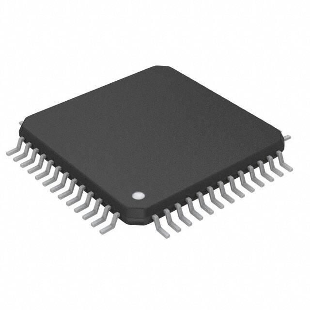
4. Ordering information
Table 2:
Ordering information
Type number
74ABT16543BB
Package
Temperature range Name
Description
Version
−40 °C to +85 °C
plastic quad flat package; 52 leads (lead length
1.6 mm); body width 10 × 10 × 2 mm
SOT379-2
QFP52
5. Functional diagram
50
51
1
2
3
5
6
7
1A0 1A1 1A2 1A3 1A4 1A5 1A6 1A7
49
1EAB
44
1EBA
1OEAB
47
48
1LEAB
1OEBA
46
45
1LEBA
1B0 1B1 1B2 1B3 1B4 1B5 1B6 1B7
42
41
39
38
37
36
35
34
8
9
10
11
12
13
15
16
2A0 2A1 2A2 2A3 2A4 2A5 2A6 2A7
18
2EAB
23
2EBA
2OEAB
20
19
2LEAB
2OEBA
21
22
2LEBA
2B0 2B1 2B2 2B3 2B4 2B5 2B6 2B7
33
32
31
29
28
27
25
24 001aad030
Fig 1. Logic symbol
9397 750 15046
Product data sheet
© Koninklijke Philips Electronics N.V. 2005. All rights reserved.
Rev. 04 — 26 May 2005
2 of 17
�74ABT16543
Philips Semiconductors
16-bit latched transceiver with dual enable; 3-state
1OEBA
1EBA
1LEBA
1OEAB
1EAB
1LEAB
1A0
46
44
45
47
49
48
1EN3
G1
1C5
2EN4
G2
2C6
50
3
6D
1A1
1A2
1A3
1A4
1A5
1A6
1A7
2OEBA
2EBA
2LEBA
2OEAB
2EAB
2LEAB
51
5D
4
42
1B0
2A0
21
23
22
20
18
19
7EN9
G7
7C11
8EN10
G8
8C12
8
9
12D
41
1
39
2
38
3
37
5
36
6
35
7
34
1B1
2A1
1B2
2A2
1B3
2A3
1B4
2A4
1B5
2A5
1B6
2A6
1B7
2A7
9
11D
10
33
32
10
31
11
29
12
28
13
27
15
25
16
24
2B0
2B1
2B2
2B3
2B4
2B5
2B6
2B7
001aad032
Fig 2. IEC logic symbol
nOEBA
nEBA
nLEBA
nOEAB
nEAB
nLEAB
LE
D
nA1
LE
8 IDENTICAL
CHANNELS
nB1
D
to 7 other channels
001aac924
Fig 3. Logic diagram
9397 750 15046
Product data sheet
© Koninklijke Philips Electronics N.V. 2005. All rights reserved.
Rev. 04 — 26 May 2005
3 of 17
�74ABT16543
Philips Semiconductors
16-bit latched transceiver with dual enable; 3-state
6. Pinning information
40 VCC
41 1B1
42 1B0
43 GND
44 1EBA
45 1LEBA
46 1OEBA
47 1OEAB
48 1LEAB
49 1EAB
50 1A0
51 1A1
52 VCC
6.1 Pinning
1A2
1
39 1B2
1A3
2
38 1B3
1A4
3
37 1B4
GND
4
36 1B5
1A5
5
35 1B6
1A6
6
1A7
7
2A0
8
32 2B1
2A1
9
31 2B2
34 1B7
16543
33 2B0
VCC 26
2B6 25
2B7 24
2EBA 23
2LEBA 22
2OEBA 21
2OEAB 20
2LEAB 19
2EAB 18
27 2B5
GND 17
28 2B4
2A5 13
2A7 16
29 2B3
2A4 12
2A6 15
30 GND
2A3 11
VCC 14
2A2 10
001aad034
Fig 4. Pin configuration QFP52
6.2 Pin description
Table 3:
Pin description
Symbol
Pin
Description
1A2
1
1 data input or output 2; A-side
1A3
2
1 data input or output 3; A-side
1A4
3
1 data input or output 4; A-side
GND
4
ground (0 V)
1A5
5
1 data input or output 5; A-side
1A6
6
1 data input or output 6; A-side
1A7
7
1 data input or output 7; A-side
2A0
8
2 data input or output 0; A-side
2A1
9
2 data input or output 1; A-side
2A2
10
2 data input or output 2; A-side
2A3
11
2 data input or output 3; A-side
2A4
12
2 data input or output 4; A-side
2A5
13
2 data input or output 5; A-side
VCC
14
supply voltage
2A6
15
2 data input or output 6; A-side
9397 750 15046
Product data sheet
© Koninklijke Philips Electronics N.V. 2005. All rights reserved.
Rev. 04 — 26 May 2005
4 of 17
�74ABT16543
Philips Semiconductors
16-bit latched transceiver with dual enable; 3-state
Table 3:
Pin description …continued
Symbol
Pin
Description
2A7
16
2 data input or output 7; A-side
GND
17
ground (0 V)
2EAB
18
A-to-B output enable input (active LOW)
2LEAB
19
A-to-B latch enable input (active LOW)
2OEAB
20
A-to-B enable input (active LOW)
2OEBA
21
B-to-A output enable input (active LOW)
2LEBA
22
B-to-A latch enable input (active LOW)
2EBA
23
B-to-A enable input (active LOW)
2B7
24
2 data input or output 7; B-side
2B6
25
2 data input or output 6; B-side
VCC
26
supply voltage
2B5
27
2 data input or output 5; B-side
2B4
28
2 data input or output 4; B-side
2B3
29
2 data input or output 3; B-side
GND
30
ground (0 V)
2B2
31
2 data input or output 2; B-side
2B1
32
2 data input or output 1; B-side
2B0
33
2 data input or output 0; B-side
1B7
34
1 data input or output 7; B-side
1B6
35
1 data input or output 6; B-side
1B5
36
1 data input or output 5; B-side
1B4
37
1 data input or output 4; B-side
1B3
38
1 data input or output 3; B-side
1B2
39
1 data input or output 2; B-side
VCC
40
positive supply voltage
1B1
41
1 data input or output 1; B-side
1B0
42
1 data input or output 0; B-side
GND
43
ground (0 V)
1EBA
44
B-to-A output enable input (active LOW)
1LEBA
45
B-to-A latch enable input (active LOW)
1OEBA
46
B-to-A enable input (active LOW)
1OEAB
47
A-to-B output enable input (active LOW)
1LEAB
48
A-to-B latch enable input (active LOW)
1EAB
49
A-to-B enable input (active LOW)
1A0
50
1 data input or output 0; A-side
1A1
51
1 data input or output 1; A-side
VCC
52
supply voltage
9397 750 15046
Product data sheet
© Koninklijke Philips Electronics N.V. 2005. All rights reserved.
Rev. 04 — 26 May 2005
5 of 17
�74ABT16543
Philips Semiconductors
16-bit latched transceiver with dual enable; 3-state
7. Functional description
7.1 Function table
Table 4:
Function table [1]
Input
Output
Status
nOEAB or
nOEBA
nEAB or
nEBA
nLEAB or
nLEBA
nAx or nBx
nBx or nAx
H
X
X
X
Z
disabled
X
H
X
X
Z
disabled
L
↑
L
h
Z
disabled + latch
L
↑
L
I
Z
disabled + latch
L
L
↑
h
H
latch + display
L
L
↑
I
L
latch + display
L
L
L
H
H
transparent
L
L
L
L
L
transparent
L
L
H
X
NC
hold
[1]
H = HIGH voltage level;
h = HIGH voltage level one set-up time prior to the LOW-to-HIGH transition of nLEAB, nLEBA, nEAB or
nEBA;
L = LOW voltage level;
l = LOW voltage level one set-up time prior to the LOW-to-HIGH transition of nLEAB, nLEBA, nEAB or
nEBA;
X = don t care;
Z = high-impedance off state;
↑ = LOW-to-HIGH transition;
NC= no change.
7.2 Description
The 74ABT16543 contains two sets of eight D-type latches, with separate control pins for
each set. Using data flow from A to B as an example, when the A-to-B enable (nEAB)
input and the A-to-B latch enable (nLEAB) input are LOW the A-to-B path is transparent.
A subsequent LOW-to-HIGH transition of the nLEAB signal puts the A data into the
latches where it is stored and the B outputs no longer change with the A inputs. With
nEAB and nOEAB both LOW, the 3-state B output buffers are active and display the data
present at the outputs of the A latches.
Control of data flow from B to A is similar, but using the nEBA, nLEBA, and nOEBA inputs.
9397 750 15046
Product data sheet
© Koninklijke Philips Electronics N.V. 2005. All rights reserved.
Rev. 04 — 26 May 2005
6 of 17
�74ABT16543
Philips Semiconductors
16-bit latched transceiver with dual enable; 3-state
8. Limiting values
Table 5:
Limiting values
In accordance with the Absolute Maximum Rating System (IEC 60134). Voltages are referenced to
GND (ground = 0 V).
Symbol
Parameter
Conditions
VCC
supply voltage
VI
input voltage
[1]
VO
output voltage
output in OFF-state or
HIGH-state
[1]
IIK
input diode current
VI < 0 V
-
−18
mA
IOK
output diode current
VO < 0 V
-
−50
mA
IO
output current
output in LOW-state
-
128
mA
-
−64
mA
output in HIGH-state
Tj
junction temperature
Tstg
storage temperature
[2]
Min
Max
Unit
−0.5
+7.0
V
−1.2
+7.0
V
−0.5
+5.5
V
-
+150
°C
−65
+150
°C
[1]
The input and output voltage ratings may be exceeded if the input and output current ratings are observed.
[2]
The performance capability of a high-performance integrated circuit in conjunction with its thermal
environment can create junction temperatures which are detrimental to reliability.
9. Recommended operating conditions
Table 6:
Recommended operating conditions
Symbol
Parameter
VCC
VI
Conditions
Min
Typ
Max
supply voltage
4.5
-
5.5
V
input voltage
0
-
VCC
V
VIH
HIGH-level input voltage
2.0
-
-
V
VIL
LOW-level input voltage
-
-
0.8
V
IOH
HIGH-level output current
-
-
−32
mA
IOL
LOW-level output current
-
-
64
mA
∆t/∆V
input transition rise or fall rate
0
-
10
ns/V
Tamb
ambient temperature
−40
-
+85
°C
in free air
9397 750 15046
Product data sheet
Unit
© Koninklijke Philips Electronics N.V. 2005. All rights reserved.
Rev. 04 — 26 May 2005
7 of 17
�74ABT16543
Philips Semiconductors
16-bit latched transceiver with dual enable; 3-state
10. Static characteristics
Table 7:
Static characteristics
At recommended operating conditions; voltages are referenced to GND (ground = 0 V)
Symbol Parameter
Conditions
Min
Typ
Max
Unit
-
-
−1.2
V
IOH = −3 mA
2.5
2.9
-
V
IOH = −32 mA
2.0
2.4
-
V
3.0
3.4
-
V
-
0.36
0.55
V
-
0.13
0.55
V
-
±0.01 ±1.0
µA
-
±2.0
±100
µA
-
±1.0
±50
µA
outputs HIGH-state at VO = 5.5 V
-
1.0
10
µA
outputs LOW-state at VO = 0.0 V
-
−1.0
−10
µA
-
1.0
50
µA
−50
−100
−200
mA
Tamb = 25 °C
VIK
input clamp voltage
VCC = 4.5 V; IIK = −18 mA
VOH
HIGH-level output voltage
VCC = 4.5 V; VI = VIL or VIH
VCC = 5.0 V; VI = VIL or VIH
IOH = −3 mA
VOL
LOW-level output voltage
VCC = 4.5 V; VI = VIL or VIH; IOL = 64 mA
VRST
power-up output voltage
VCC = 5.5 V; IO = 1 mA; VI = GND or VCC
ILI
input leakage current of
control pins
VCC = 5.5 V; VI = GND or 5.5 V
IOFF
power-off leakage current
VCC = 0.0 V; VO or VI ≤ 4.5 V
IPU, IPD
power-up or power-down
down 3-state output current
VCC = 2.1 V; VO = 0.0 V or VCC; VI = GND or
VCC; VnOEAB and VnOEBA = don’t care
IOZ
3-state output current
VCC = 5.5 V; VI = VIL or VIH
[1]
[2]
ICEX
output HIGH leakage current VCC = 5.5 V; VO = 5.5 V; VI = GND or VCC
IO
output current
VCC = 5.5 V; VO = 2.5 V
CI
input capacitance
VI = 0 V or VCC
-
3
-
pF
CI/O
I/O capacitance
VO = 0 V or VCC; 3-state
-
7
-
pF
ICC
quiescent supply current
VCC = 5.5 V; VI = GND or VCC
outputs HIGH-state
-
0.55
2
mA
outputs LOW-state
-
9
19
mA
-
0.55
2
mA
-
5.0
50
µA
-
-
−1.2
V
IOH = −3 mA
2.5
-
-
V
IOH = −32 mA
2.0
-
-
V
3.0
-
-
V
0.55
V
[3]
outputs 3-state
∆ICC
additional supply current per
input pin
VCC = 5.5 V; one input at 3.4 V; other inputs
at VCC or GND
[4]
Tamb = −40 °C to +85 °C
VIK
input clamp voltage
VCC = 4.5 V; IIK = −18 mA
VOH
HIGH-level output voltage
VCC = 4.5 V; VI = VIL or VIH
VCC = 5.0 V; VI = VIL or VIH
IOH = −3 mA
VOL
LOW-level output voltage
VCC = 4.5 V; VI = VIL or VIH; IOL = 64 mA
VRST
power-up output voltage
VCC = 5.5 V; IO = 1 mA; VI = GND or VCC
ILI
input leakage current of
control pins
IOFF
power-off leakage current
-
-
0.55
V
VCC = 5.5 V; VI = GND or 5.5 V
-
-
±1.0
µA
VCC = 0.0 V; VO or VI ≤ 4.5 V
-
-
±100
µA
9397 750 15046
Product data sheet
[1]
© Koninklijke Philips Electronics N.V. 2005. All rights reserved.
Rev. 04 — 26 May 2005
8 of 17
�74ABT16543
Philips Semiconductors
16-bit latched transceiver with dual enable; 3-state
Table 7:
Static characteristics …continued
At recommended operating conditions; voltages are referenced to GND (ground = 0 V)
Symbol Parameter
Conditions
Min
Typ
Max
Unit
-
-
±50
µA
outputs HIGH-state at VO = 5.5 V
-
-
10
µA
outputs LOW-state at VO = 0.0 V
-
-
−10
µA
-
-
50
µA
−50
-
−200
mA
outputs HIGH-state
-
-
2
mA
outputs LOW-state
-
-
19
mA
IPU, IPD
power-up or power-down
down 3-state output current
VCC = 2.1 V; VO = 0.0 V or VCC; VI = GND or
VCC; VnOEAB and VnOEBA = don’t care
IOZ
3-state output current
VCC = 5.5 V; VI = VIL or VIH
ICEX
[2]
output HIGH leakage current VCC = 5.5 V; VO = 5.5 V; VI = GND or VCC
IO
output current
VCC = 5.5 V; VO = 2.5 V
ICC
quiescent supply current
VCC = 5.5 V; VI = GND or VCC
[3]
outputs 3-state
∆ICC
additional supply current per
input pin
VCC = 5.5 V; one input at 3.4 V; other inputs
at VCC or GND
[4]
-
-
2
mA
-
-
50
µA
[1]
For valid test results, data must not be loaded into the latches after applying the power.
[2]
This parameter is valid for any VCC between 0 V and 2.1 V, with a transition time of up to 10 ms; From VCC = 2.1 V to VCC = 5 V ± 10 %
a transition time of up to 100 µs is permitted.
[3]
Not more than one output should be tested at a time, and the duration of the test should not exceed one second.
[4]
This is the increase in supply current for each input at 3.4 V.
11. Dynamic characteristics
Table 8:
Dynamic characteristics
GND = 0 V; for test circuit see Figure 10.
Symbol Parameter
Conditions
Min
Typ
Max
Unit
nAx to nBx, nBx to nAx
see Figure 6
1.0
2.5
3.3
ns
nLEBA to nAx, nLEAB to nBx
see Figure 5
1.0
3.1
4.3
ns
nAx to nBx, nBx to nAx
see Figure 6
1.0
2.2
4.4
ns
nLEBA to nAx, nLEAB to nBx
see Figure 5
1.2
3.0
4.8
ns
nOEBA to nAx, nOEAB to nBx
1.0
3.3
4.3
ns
nEBA to nAx, nEAB to nBx
1.0
3.4
4.9
ns
1.1
3.3
5.9
ns
1.2
3.4
6.5
ns
nOEBA to nAx, nOEAB to nBx
1.9
3.5
5.0
ns
nEBA to nAx, nEAB to nBx
2.0
3.4
5.6
ns
Tamb = 25 °C; VCC = 5.0 V
tPLH
tPHL
tPZH
tPZL
propagation delay
propagation delay
output enable time
output enable time
see Figure 7
see Figure 8
nOEBA to nAx, nOEAB to nBx
nEBA to nAx, nEAB to nBx
tPHZ
output disable time
see Figure 7
9397 750 15046
Product data sheet
© Koninklijke Philips Electronics N.V. 2005. All rights reserved.
Rev. 04 — 26 May 2005
9 of 17
�74ABT16543
Philips Semiconductors
16-bit latched transceiver with dual enable; 3-state
Table 8:
Dynamic characteristics …continued
GND = 0 V; for test circuit see Figure 10.
Symbol Parameter
Conditions
Min
Typ
Max
Unit
tPLZ
see Figure 8
1.6
2.6
4.2
ns
1.7
2.6
5.1
ns
nAx to nLEAB, nBx to nLEBA
1.5
0.4
-
ns
nAx to nEAB, nBx to nEBA
1.5
0.2
-
ns
nAx to nLEAB, nBx to nLEBA
+3.5
−0.1
-
ns
nAx to nEAB, nBx to nEBA
+3.5
−0.3
-
ns
nAx to nLEAB, nBx to nLEBA
1.5
0.2
-
ns
nAx to nEAB, nBx to nEBA
1.5
0.3
-
ns
+2.0
−0.3
-
ns
output disable time
nOEBA to nAx, nOEAB to nBx
nEBA to nAx, nEAB to nBx
tsu(H)
tsu(L)
th(H)
th(L)
set-up time HIGH
set-up time LOW
hold time HIGH
hold time LOW
see Figure 9
see Figure 9
see Figure 9
see Figure 9
nAx to nLEAB, nBx to nLEBA
+2.0
−0.2
-
ns
see Figure 9
4.0
3.1
-
ns
nAx to nBx, nBx to nAx
see Figure 6
1.0
-
3.8
ns
nLEBA to nAx, nLEAB to nBx
see Figure 5
1.0
-
5.2
ns
nAx to nBx, nBx to nAx
see Figure 6
1.0
-
5.1
ns
nLEBA to nAx, nLEAB to nBx
see Figure 5
1.2
-
5.6
ns
nOEBA to nAx, nOEAB to nBx
1.0
-
5.2
ns
nEBA to nAx, nEAB to nBx
1.0
-
6.2
ns
nOEBA to nAx, nOEAB to nBx
1.1
-
7.0
ns
nEBA to nAx, nEAB to nBx
1.2
-
7.8
ns
nOEBA to nAx, nOEAB to nBx
1.9
-
5.7
ns
nEBA to nAx, nEAB to nBx
2.0
-
6.6
ns
1.6
-
4.6
ns
1.7
-
5.4
ns
nAx to nLEAB, nBx to nLEBA
1.5
-
-
ns
nAx to nEAB, nBx to nEBA
1.5
-
-
ns
nAx to nEAB, nBx to nEBA
tWL
pulse width LOW
Tamb = −40 °C to +85 °C; VCC = 5.0 V ± 0.5 V
tPLH
tPHL
tPZH
tPZL
tPHZ
tPLZ
propagation delay
propagation delay
output enable time
output enable time
output disable time
output disable time
see Figure 7
see Figure 8
see Figure 7
see Figure 8
nOEBA to nAx, nOEAB to nBx
nEBA to nAx, nEAB to nBx
tsu(H)
set-up time HIGH
see Figure 9
9397 750 15046
Product data sheet
© Koninklijke Philips Electronics N.V. 2005. All rights reserved.
Rev. 04 — 26 May 2005
10 of 17
�74ABT16543
Philips Semiconductors
16-bit latched transceiver with dual enable; 3-state
Table 8:
Dynamic characteristics …continued
GND = 0 V; for test circuit see Figure 10.
Symbol Parameter
Conditions
Min
Typ
Max
Unit
tsu(L)
see Figure 9
3.5
-
-
ns
3.5
-
-
ns
nAx to nLEAB, nBx to nLEBA
1.5
-
-
ns
nAx to nEAB, nBx to nEBA
1.5
-
-
ns
nAx to nLEAB, nBx to nLEBA
2.0
-
-
ns
nAx to nEAB, nBx to nEBA
2.0
-
-
ns
4.0
-
-
ns
set-up time LOW
nAx to nLEAB, nBx to nLEBA
nAx to nEAB, nBx to nEBA
th(H)
th(L)
tWL
hold time HIGH
see Figure 9
hold time LOW
see Figure 9
pulse width LOW
see Figure 9
12. Waveforms
3.0 V
VM
VM
nLEAB or nLEBA
GND
t PHL
t PLH
VOH
VM
nAx or nBx
VM
VOL
001aac925
VM = 1.5 V.
VOL and VOH are typical voltage output drop that occur with the output load.
Fig 5. Inverting input to output propagation delay
3.0 V
nAx or nBx
VM
VM
GND
t PLH
t PHL
VOH
nBx or nAx
VM
VM
VOL
001aac926
VM = 1.5 V.
VOL and VOH are typical voltage output drop that occur with the output load.
Fig 6. Non-inverting input to output propagation delay
9397 750 15046
Product data sheet
© Koninklijke Philips Electronics N.V. 2005. All rights reserved.
Rev. 04 — 26 May 2005
11 of 17
�74ABT16543
Philips Semiconductors
16-bit latched transceiver with dual enable; 3-state
3.0 V
nOEAB, nOEBA,
VM
VM
nEAB, nEBA
GND
t PZH
t PHZ
VOH
nAx or nBx output
VOH − 0.3 V
VM
VOL
001aac929
VM = 1.5 V.
VOL and VOH are typical voltage output drop that occur with the output load.
Fig 7. 3-state output enable time to HIGH-level and output disable time from HIGH-level
state
3.0 V
nOEAB, nOEBA,
VM
VM
nEAB, nEBA
GND
t PZL
t PLZ
VOH
nAx or nBx output
VM
VOL + 0.3 V
VOL
001aac928
VM = 1.5 V.
VOL and VOH are typical voltage output drop that occur with the output load.
Fig 8. 3-state output enable time to LOW-level and output disable time from LOW-level
state
3.0 V
nAx, nBx
VM
VM
VM
VM
GND
t su(H)
t h(H)
t su(L)
t h(L)
t WL
3.0 V
nLEAB, nLEBA,
VM
VM
nEAB, nEBA
GND
001aac927
VM = 1.5 V.
The shaded areas indicate when the input is permitted to change for predictable output
performance.
Fig 9. Data set-up and hold times and latch enable pulse width
9397 750 15046
Product data sheet
© Koninklijke Philips Electronics N.V. 2005. All rights reserved.
Rev. 04 — 26 May 2005
12 of 17
�74ABT16543
Philips Semiconductors
16-bit latched transceiver with dual enable; 3-state
VI
tW
90 %
negative
pulse
90 %
VM
0V
VI
tTHL(tf)
tTLH(tr)
tTLH(tr)
tTHL(tf)
90 %
positive
pulse
0V
VM
10 %
VM
VM
10 %
10 %
tW
001aac221
VM = 1.5 V.
a. Input pulse definition
VEXT
VCC
PULSE
GENERATOR
VI
RL
VO
DUT
CL
RT
RL
mna616
Test data is given in Table 9.
Definitions test circuit:
RL = Load resistor.
CL = Load capacitance including jig and probe capacitance.
RT = Termination resistance should be equal to output impedance Zo of the pulse generator.
VEXT = Test voltage for switching times.
b. Test circuit
Fig 10. Load circuitry for switching times
Table 9:
Test data
Input
Load
VI
fi
tW
tr, tf
CL
RL
tPHZ, tPZH tPLZ, tPZL tPLH, tPHL
3.0 V
1 MHz
500 ns
≤ 2.5 ns
50 pF
500 Ω
open
9397 750 15046
Product data sheet
VEXT
7.0 V
open
© Koninklijke Philips Electronics N.V. 2005. All rights reserved.
Rev. 04 — 26 May 2005
13 of 17
�74ABT16543
Philips Semiconductors
16-bit latched transceiver with dual enable; 3-state
13. Package outline
QFP52: plastic quad flat package; 52 leads (lead length 1.6 mm); body 10 x 10 x 2 mm
SOT379-2
c
y
X
A
27
39
40
ZE
26
e
E HE
A
A2
(A 3)
A1
wM
θ
bp
Lp
pin 1 index
L
14
52
detail X
13
1
v M A
ZD
e
wM
bp
D
B
HD
v M B
0
2.5
5 mm
scale
DIMENSIONS (mm are the original dimensions)
UNIT
A
max.
A1
A2
A3
bp
c
D(1)
E(1)
e
mm
2.45
0.25
0.10
2.2
1.8
0.25
0.40
0.22
0.23
0.11
10.1
9.9
10.1
9.9
0.65
HD
HE
13.45 13.45
12.95 12.95
L
Lp
v
w
y
1.6
1.03
0.73
0.2
0.13
0.1
ZD(1) ZE(1)
θ
1.31
0.90
7o
o
0
1.31
0.90
Note
1. Plastic or metal protrusions of 0.25 mm maximum per side are not included.
OUTLINE
VERSION
SOT379-2
REFERENCES
IEC
JEDEC
JEITA
EUROPEAN
PROJECTION
ISSUE DATE
99-11-03
03-02-25
MS-022
Fig 11. Package outline SOT379-2 (QFP52)
9397 750 15046
Product data sheet
© Koninklijke Philips Electronics N.V. 2005. All rights reserved.
Rev. 04 — 26 May 2005
14 of 17
�74ABT16543
Philips Semiconductors
16-bit latched transceiver with dual enable; 3-state
14. Revision history
Table 10:
Revision history
Document ID
Release date
Data sheet status
Change notice
Doc. number
Supersedes
74ABT16543_4
20050526
Product data sheet
-
9397 750 15046
74ABT16543_3
Modifications:
74ABT16543_3
•
The format of this data sheet has been redesigned to comply with the new presentation and
information standard of Philips Semiconductors.
•
•
Section 2 “Features”: Changed JEDEC Std 17 to JEDEC Std 78
QFP52 package information added to and (T)SSOP56 packages removed from Section 4
“Ordering information”, Section 5 “Functional diagram”, Section 6 “Pinning information” and
Section 13 “Package outline”
20020403
Product data sheet
-
9397 750 15046
Product data sheet
9397 750 09692
-
© Koninklijke Philips Electronics N.V. 2005. All rights reserved.
Rev. 04 — 26 May 2005
15 of 17
�74ABT16543
Philips Semiconductors
16-bit latched transceiver with dual enable; 3-state
15. Data sheet status
Level
Data sheet status [1]
Product status [2] [3]
Definition
I
Objective data
Development
This data sheet contains data from the objective specification for product development. Philips
Semiconductors reserves the right to change the specification in any manner without notice.
II
Preliminary data
Qualification
This data sheet contains data from the preliminary specification. Supplementary data will be published
at a later date. Philips Semiconductors reserves the right to change the specification without notice, in
order to improve the design and supply the best possible product.
III
Product data
Production
This data sheet contains data from the product specification. Philips Semiconductors reserves the
right to make changes at any time in order to improve the design, manufacturing and supply. Relevant
changes will be communicated via a Customer Product/Process Change Notification (CPCN).
[1]
Please consult the most recently issued data sheet before initiating or completing a design.
[2]
The product status of the device(s) described in this data sheet may have changed since this data sheet was published. The latest information is available on the Internet at
URL http://www.semiconductors.philips.com.
[3]
For data sheets describing multiple type numbers, the highest-level product status determines the data sheet status.
16. Definitions
customers using or selling these products for use in such applications do so
at their own risk and agree to fully indemnify Philips Semiconductors for any
damages resulting from such application.
Short-form specification — The data in a short-form specification is
extracted from a full data sheet with the same type number and title. For
detailed information see the relevant data sheet or data handbook.
Right to make changes — Philips Semiconductors reserves the right to
make changes in the products - including circuits, standard cells, and/or
software - described or contained herein in order to improve design and/or
performance. When the product is in full production (status ‘Production’),
relevant changes will be communicated via a Customer Product/Process
Change Notification (CPCN). Philips Semiconductors assumes no
responsibility or liability for the use of any of these products, conveys no
license or title under any patent, copyright, or mask work right to these
products, and makes no representations or warranties that these products are
free from patent, copyright, or mask work right infringement, unless otherwise
specified.
Limiting values definition — Limiting values given are in accordance with
the Absolute Maximum Rating System (IEC 60134). Stress above one or
more of the limiting values may cause permanent damage to the device.
These are stress ratings only and operation of the device at these or at any
other conditions above those given in the Characteristics sections of the
specification is not implied. Exposure to limiting values for extended periods
may affect device reliability.
Application information — Applications that are described herein for any
of these products are for illustrative purposes only. Philips Semiconductors
make no representation or warranty that such applications will be suitable for
the specified use without further testing or modification.
18. Trademarks
17. Disclaimers
Notice — All referenced brands, product names, service names and
trademarks are the property of their respective owners.
Life support — These products are not designed for use in life support
appliances, devices, or systems where malfunction of these products can
reasonably be expected to result in personal injury. Philips Semiconductors
19. Contact information
For additional information, please visit: http://www.semiconductors.philips.com
For sales office addresses, send an email to: sales.addresses@www.semiconductors.philips.com
9397 750 15046
Product data sheet
© Koninklijke Philips Electronics N.V. 2005. All rights reserved.
Rev. 04 — 26 May 2005
16 of 17
�74ABT16543
Philips Semiconductors
16-bit latched transceiver with dual enable; 3-state
20. Contents
1
2
3
4
5
6
6.1
6.2
7
7.1
7.2
8
9
10
11
12
13
14
15
16
17
18
19
General description . . . . . . . . . . . . . . . . . . . . . . 1
Features . . . . . . . . . . . . . . . . . . . . . . . . . . . . . . . 1
Quick reference data . . . . . . . . . . . . . . . . . . . . . 1
Ordering information . . . . . . . . . . . . . . . . . . . . . 2
Functional diagram . . . . . . . . . . . . . . . . . . . . . . 2
Pinning information . . . . . . . . . . . . . . . . . . . . . . 4
Pinning . . . . . . . . . . . . . . . . . . . . . . . . . . . . . . . 4
Pin description . . . . . . . . . . . . . . . . . . . . . . . . . 4
Functional description . . . . . . . . . . . . . . . . . . . 6
Function table . . . . . . . . . . . . . . . . . . . . . . . . . . 6
Description . . . . . . . . . . . . . . . . . . . . . . . . . . . . 6
Limiting values. . . . . . . . . . . . . . . . . . . . . . . . . . 7
Recommended operating conditions. . . . . . . . 7
Static characteristics. . . . . . . . . . . . . . . . . . . . . 8
Dynamic characteristics . . . . . . . . . . . . . . . . . . 9
Waveforms . . . . . . . . . . . . . . . . . . . . . . . . . . . . 11
Package outline . . . . . . . . . . . . . . . . . . . . . . . . 14
Revision history . . . . . . . . . . . . . . . . . . . . . . . . 15
Data sheet status . . . . . . . . . . . . . . . . . . . . . . . 16
Definitions . . . . . . . . . . . . . . . . . . . . . . . . . . . . 16
Disclaimers . . . . . . . . . . . . . . . . . . . . . . . . . . . . 16
Trademarks. . . . . . . . . . . . . . . . . . . . . . . . . . . . 16
Contact information . . . . . . . . . . . . . . . . . . . . 16
© Koninklijke Philips Electronics N.V. 2005
All rights are reserved. Reproduction in whole or in part is prohibited without the prior
written consent of the copyright owner. The information presented in this document does
not form part of any quotation or contract, is believed to be accurate and reliable and may
be changed without notice. No liability will be accepted by the publisher for any
consequence of its use. Publication thereof does not convey nor imply any license under
patent- or other industrial or intellectual property rights.
Date of release: 26 May 2005
Document number: 9397 750 15046
Published in The Netherlands
�


 工商网监
湘ICP备2023018690号
工商网监
湘ICP备2023018690号