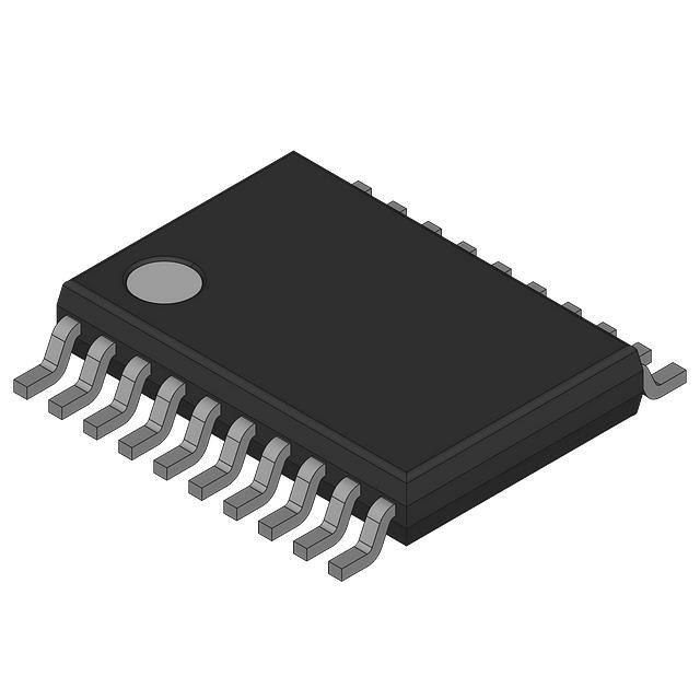
74LVT244B; 74LVTH244B
3.3 V octal buffer/line driver; 3-state
Rev. 03 — 3 March 2006
Product data sheet
1. General description
The 74LVT244B; 74LVTH244B is a high-performance BiCMOS product designed for VCC
operation at 3.3 V.
This device is an octal buffer that is ideal for driving bus lines. The device features two
output enable inputs (1OE and 2OE), each controlling four of the 3-state outputs.
2. Features
n
n
n
n
n
n
n
n
n
n
n
Octal bus interface
3-state buffers
Speed upgrade of 74LVT244A
Output capability: +64 mA and −32 mA
TTL input and output switching levels
Input and output interface capability to systems at 5 V supply
Bus hold data inputs eliminate need for external pull-up resistors to hold unused inputs
Power-up 3-state
Live insertion and extraction permitted
No bus current loading when output is tied to 5 V bus
Latch-up protection:
u JESD78: exceeds 500 mA
n ESD protection:
u HBM EIA/JESD22-A114-C exceeds 2000 V
u MM EIA/JESD22-A115-A 200 V
3. Quick reference data
Table 1.
Quick reference data
GND = 0 V; Tamb = 25 °C.
Symbol Parameter
Conditions
Min
Typ
Max
Unit
tPLH
LOW-to-HIGH propagation
delay nAn to nYn
CL = 50 pF; VCC = 3.3 V
-
1.9
-
ns
tPHL
HIGH-to-LOW propagation CL = 50 pF; VCC = 3.3 V
delay nAn to nYn
-
2.0
-
ns
�74LVT244B; 74LVTH244B
Philips Semiconductors
3.3 V octal buffer/line driver; 3-state
Table 1.
Quick reference data …continued
GND = 0 V; Tamb = 25 °C.
Symbol Parameter
Conditions
Min
Typ
Max
Unit
Ci
input capacitance
VI = 0 V or 3.0 V
-
4
-
pF
Co
output capacitance
outputs disabled;
VO = 0 V or 3.0 V
-
8
-
pF
ICC
quiescent supply current
outputs disabled;
VCC = 3.6 V; IO = 0 A;
VI = GND or VCC
-
0.13
-
mA
4. Ordering information
Table 2.
Ordering information
Type number
Package
Temperature range Name
Description
Version
74LVT244BD
−40 °C to +85 °C
SO20
plastic small outline package; 20 leads;
body width 7.5 mm
SOT163-1
74LVT244BDB
−40 °C to +85 °C
SSOP20
plastic shrink small outline package; 20 leads;
body width 5.3 mm
SOT339-1
74LVT244BPW
−40 °C to +85 °C
TSSOP20
plastic thin shrink small outline package; 20 leads;
body width 4.4 mm
SOT360-1
74LVTH244BD
−40 °C to +85 °C
SO20
plastic small outline package; 20 leads;
body width 7.5 mm
SOT163-1
74LVTH244BDB
−40 °C to +85 °C
SSOP20
plastic shrink small outline package; 20 leads;
body width 5.3 mm
SOT339-1
74LVTH244BPW
−40 °C to +85 °C
TSSOP20
plastic thin shrink small outline package; 20 leads;
body width 4.4 mm
SOT360-1
74LVT_LVTH244B_3
Product data sheet
© Koninklijke Philips Electronics N.V. 2006. All rights reserved.
Rev. 03 — 3 March 2006
2 of 15
�74LVT244B; 74LVTH244B
Philips Semiconductors
3.3 V octal buffer/line driver; 3-state
5. Functional diagram
2
4
1A0
1Y0
1A1
1Y1
1A2
1Y2
1A3
1Y3
18
16
1
6
8
1
11
13
15
17
19
12
1OE
2A0
2A1
2Y0
9
2Y1
2A2
2Y2
2A3
2Y3
EN
14
2
18
4
16
6
14
8
12
19
7
5
EN
11
9
13
7
15
5
17
3
3
mna826
2OE
mna825
Fig 1. Logic symbol
Fig 2. IEC logic symbol
6. Pinning information
6.1 Pinning
74LVT244B
74LVTH244B
1OE
1
20 VCC
1A0
2
19 2OE
2Y3
3
18 1Y0
1A1
4
17 2A3
2Y2
5
16 1Y1
1A2
6
15 2A2
2Y1
7
14 1Y2
1A3
8
13 2A1
2Y0
9
12 1Y3
GND 10
11 2A0
001aae463
Fig 3. Pin configuration SO20, SSOP20 and TSSOP20
74LVT_LVTH244B_3
Product data sheet
© Koninklijke Philips Electronics N.V. 2006. All rights reserved.
Rev. 03 — 3 March 2006
3 of 15
�74LVT244B; 74LVTH244B
Philips Semiconductors
3.3 V octal buffer/line driver; 3-state
6.2 Pin description
Table 3.
Pin description
Symbol
Pin
Description
1OE
1
1 output enable input
1A0
2
1 data input 0
2Y3
3
2 data output 3
1A1
4
1 data input 1
2Y2
5
2 data output 2
1A2
6
1 data input 2
2Y1
7
2 data output 1
1A3
8
1 data input 3
2Y0
9
2 data output 0
GND
10
ground (0 V)
2A0
11
2 data input 0
1Y3
12
1 data output 3
2A1
13
2 data input 1
1Y2
14
1 data output 2
2A2
15
2 data input 2
1Y1
16
1 data output 1
2A3
17
2 data input 3
1Y0
18
1 data output 0
2OE
19
2 output enable input
VCC
20
supply voltage
7. Functional description
7.1 Function table
Table 4.
Function table [1]
Control
Input
Output
nOE
nAn
nYn
L
L
L
H
H
X
Z
H
[1]
H = HIGH voltage level;
L = LOW voltage level;
X = don’t care;
Z = high-impedance OFF-state.
74LVT_LVTH244B_3
Product data sheet
© Koninklijke Philips Electronics N.V. 2006. All rights reserved.
Rev. 03 — 3 March 2006
4 of 15
�74LVT244B; 74LVTH244B
Philips Semiconductors
3.3 V octal buffer/line driver; 3-state
8. Limiting values
Table 5.
Limiting values
In accordance with the Absolute Maximum Rating System (IEC 60134). Voltages are referenced to
GND (ground = 0 V).
Symbol Parameter
Conditions
Min
Max
Unit
VCC
supply voltage
−0.5
+4.6
V
VI
input voltage
[1]
−0.5
+7.0
V
VO
output voltage
[1]
−0.5
+7.0
V
output in OFF-state or
HIGH-state
IIK
input clamping current
VI < 0 V
-
−50
mA
IOK
output clamping current
VO < 0 V
-
−50
mA
IO
output current
output in LOW-state
-
128
mA
output in HIGH-state
-
−64
mA
−65
+150
°C
-
150
°C
Tstg
storage temperature
Tj
junction temperature
[2]
[1]
The input and output negative voltage ratings may be exceeded if the input and output clamp current ratings
are observed.
[2]
The performance capability of a high-performance integrated circuit in conjunction with its thermal
environment can create junction temperatures which are detrimental to reliability.
9. Recommended operating conditions
Table 6.
Recommended operating conditions
Symbol Parameter
Conditions
Typ
Max
Unit
VCC
supply voltage
2.7
-
3.6
V
VI
input voltage
0
-
5.5
V
VIH
HIGH-state input voltage
2.0
-
-
V
VIL
LOW-state input voltage
-
-
0.8
V
IOH
HIGH-state output current
-
-
−32
mA
IOL
LOW-state output current
none
-
-
32
mA
current duty cycle ≤ 50 %;
fi ≥ 1 kHz
-
-
64
mA
Tamb
ambient temperature
in free-air
−40
-
+85
°C
∆t/∆V
input transition rise and
fall rate
outputs enabled
-
-
10
ns/V
74LVT_LVTH244B_3
Product data sheet
Min
© Koninklijke Philips Electronics N.V. 2006. All rights reserved.
Rev. 03 — 3 March 2006
5 of 15
�74LVT244B; 74LVTH244B
Philips Semiconductors
3.3 V octal buffer/line driver; 3-state
10. Static characteristics
Table 7.
Static characteristics
At recommended operating conditions; voltages are referenced to GND (ground = 0 V).
Symbol Parameter
Tamb = −40 °C to +85 °C
Conditions
Min
Typ
Max
Unit
-
−0.9
−1.2
V
IOH = −100 µA
VCC − 2.0
VCC − 2.1
-
V
IOH = −8 mA
2.4
2.5
-
V
2.0
2.2
-
V
IOL = 100 µA
-
0.1
0.2
V
IOL = 24 mA
-
0.3
0.5
V
IOL = 16 mA
-
0.25
0.4
V
IOL = 32 mA
-
0.3
0.5
V
IOL = 64 mA
-
0.4
0.55
V
-
0.1
10
µA
-
±0.1
±1
µA
VI = VCC
-
0.1
1
µA
VI = 0 V
-
−1
−5
µA
-
1
±100
µA
VI = 0.8 V
75
130
-
µA
VI = 2.0 V
−75
−140
-
µA
[1]
VIK
input clamping voltage
VCC = 2.7 V; IIK = −18 mA
VOH
HIGH-state output voltage
VCC = 2.7 V
VCC = 3.0 V
IOH = −32 mA
VOL
LOW-state output voltage
VCC = 2.7 V
VCC = 3.0 V
ILI
input leakage current
all pins
VCC = 0 V or 3.6 V; VI = 5.5 V
control pins
VCC = 3.6 V; VI = VCC or GND
I/O data pins
IOFF
IHOLD
power-off leakage current
bus hold current data input
VCC = 3.6 V
[2]
VCC = 0 V; VI or VO = 0 V to 4.5 V
[3]
VCC = 3 V
VCC = 0 V to 3.6 V
±500
-
-
µA
-
60
125
µA
-
±1
±100
µA
output HIGH: VO = 3.0 V
-
1
5
µA
output LOW: VO = 0.5 V
-
−1
−5
µA
-
0.13
0.19
mA
-
2
5
mA
-
0.13
0.19
mA
VI = 3.6 V
IEX
external current into output
output in HIGH-state when
VO > VCC; VO = 5.5 V; VCC = 3.3 V
IO(pu/pd)
power-up/power-down
output current
VCC ≤ 1.2 V; VO = 0.5 V to VCC;
VI = GND or VCC; nOE = don’t care
IOZ
OFF-state output current
VCC = 3.6 V; VI = VIH or VIL
ICC
quiescent supply current
[4]
VCC = 3.6 V; VI = GND or VCC;
IO = 0 A
output HIGH
output LOW
outputs disabled
74LVT_LVTH244B_3
Product data sheet
[5]
© Koninklijke Philips Electronics N.V. 2006. All rights reserved.
Rev. 03 — 3 March 2006
6 of 15
�74LVT244B; 74LVTH244B
Philips Semiconductors
3.3 V octal buffer/line driver; 3-state
Table 7.
Static characteristics …continued
At recommended operating conditions; voltages are referenced to GND (ground = 0 V).
Symbol Parameter
Conditions
Min
Typ
Max
Unit
-
0.1
0.2
mA
∆ICC
additional quiescent supply
current
per input pin; VCC = 3.0 V to 3.6 V;
one input at VCC − 0.6 V and other
inputs at VCC or GND
Ci
input capacitance
VI = 0 V or 3.0 V
-
4
-
pF
Co
output capacitance
outputs disabled; VO = 0 V or 3.0 V
-
8
-
pF
[6]
[1]
Typical values are measured at Tamb = 25 °C.
[2]
Unused pins at VCC or GND.
[3]
This is the bus hold overdrive current required to force the input to the opposite logic state.
[4]
This parameter is valid for any VCC between 0 V and 1.2 V with a transition time of up to 10 ms. From VCC = 1.2 V to VCC = 3.3 V ± 0.3 V
a transition time of 100 µs is permitted. This parameter is valid for Tamb = 25 °C only.
[5]
ICC is measured with outputs pulled to VCC or GND.
[6]
This is the increase in supply current for each input at VCC − 0.6 V.
11. Dynamic characteristics
Table 8.
Dynamic characteristics
Voltages are referenced to GND (ground = 0 V); for test circuit see Figure 6.
Symbol
Parameter
Tamb = −40 °C to +85 °C
tPLH
Conditions
LOW-to-HIGH propagation delay
nAn to nYn
HIGH-to-LOW propagation delay
nAn to nYn
tPHL
tPZH
output enable time to HIGH-level
nOE to nYn
output enable time to LOW-level
nOE to nYn
tPZL
Min
Typ
Max
Unit
VCC = 2.7 V
-
-
3.8
ns
VCC = 3.0 V to 3.6 V
1.1
1.9
3.5
ns
VCC = 2.7 V
-
-
3.6
ns
VCC = 3.0 V to 3.6 V
1.3
2.0
3.3
ns
VCC = 2.7 V
-
-
5.3
ns
VCC = 3.0 V to 3.6 V
1.1
2.8
4.5
ns
VCC = 2.7 V
-
-
4.9
ns
VCC = 3.0 V to 3.6 V
1.4
2.3
4.4
ns
-
-
4.5
ns
1.9
2.9
4.4
ns
VCC = 2.7 V
-
-
4.4
ns
VCC = 3.0 V to 3.6 V
1.8
2.5
4.4
ns
[1]
see Figure 4
see Figure 4
see Figure 5
see Figure 5
output disable time from HIGH-level see Figure 5
nOE to nYn
VCC = 2.7 V
tPHZ
VCC = 3.0 V to 3.6 V
output disable time from LOW-level
nOE to nYn
tPLZ
[1]
see Figure 5
Typical values are measured at VCC = 3.3 V and Tamb = 25 °C.
74LVT_LVTH244B_3
Product data sheet
© Koninklijke Philips Electronics N.V. 2006. All rights reserved.
Rev. 03 — 3 March 2006
7 of 15
�74LVT244B; 74LVTH244B
Philips Semiconductors
3.3 V octal buffer/line driver; 3-state
12. Waveforms
VI
nAn input
VM
VM
GND
tPLH
tPHL
VOH
VM
nYn output
VM
VOL
mna171
Measurement points are given in Table 9.
VOL and VOH are typical voltage output drop that occur with the output load.
Fig 4. Propagation delay input (nAn) to output (nYn)
VI
nOE input
VM
GND
tPZL
tPLZ
3.0 V
VM
nYn output
VX
VOL
t PZH
t PHZ
VOH
nYn output
VY
VM
0V
001aae464
Measurement points are given in Table 9.
VOL and VOH are typical voltage output drop that occur with the output load.
Fig 5. 3-state output enable and disable times
Table 9.
Measurement points
Input
Output
VM
VM
VX
VY
1.5 V
1.5 V
VOL + 0.3 V
VOH − 0.3 V
74LVT_LVTH244B_3
Product data sheet
© Koninklijke Philips Electronics N.V. 2006. All rights reserved.
Rev. 03 — 3 March 2006
8 of 15
�74LVT244B; 74LVTH244B
Philips Semiconductors
3.3 V octal buffer/line driver; 3-state
VI
tW
90 %
negative
pulse
VM
0V
VI
tf
tr
tr
tf
90 %
positive
pulse
0V
VM
10 %
VM
VM
10 %
tW
VEXT
VCC
PULSE
GENERATOR
VI
RL
VO
DUT
RT
CL
RL
001aae235
Test data is given in Table 10.
Definitions test circuit:
RL = Load resistor.
CL = Load capacitance including jig and probe capacitance.
RT = Termination resistance should be equal to output impedance Zo of the pulse generator.
VEXT = Test voltage for switching times.
Fig 6. Load circuitry for switching times
Table 10.
Test data
Input
Load
VI
fi
tW
tr, tf
2.7 V
≤ 10 MHz 500 ns
CL
≤ 2.5 ns 50 pF
74LVT_LVTH244B_3
Product data sheet
VEXT
RL
tPHZ, tPZH
tPLZ, tPZL
tPLH, tPHL
500 Ω
GND
6V
open
© Koninklijke Philips Electronics N.V. 2006. All rights reserved.
Rev. 03 — 3 March 2006
9 of 15
�74LVT244B; 74LVTH244B
Philips Semiconductors
3.3 V octal buffer/line driver; 3-state
13. Package outline
SO20: plastic small outline package; 20 leads; body width 7.5 mm
SOT163-1
D
E
A
X
c
HE
y
v M A
Z
20
11
Q
A2
A
(A 3)
A1
pin 1 index
θ
Lp
L
10
1
e
detail X
w M
bp
0
5
10 mm
scale
DIMENSIONS (inch dimensions are derived from the original mm dimensions)
UNIT
A
max.
A1
A2
A3
bp
c
D (1)
E (1)
e
HE
L
Lp
Q
v
w
y
mm
2.65
0.3
0.1
2.45
2.25
0.25
0.49
0.36
0.32
0.23
13.0
12.6
7.6
7.4
1.27
10.65
10.00
1.4
1.1
0.4
1.1
1.0
0.25
0.25
0.1
0.01
0.019 0.013
0.014 0.009
0.51
0.49
0.30
0.29
0.05
0.419
0.043
0.055
0.394
0.016
inches
0.1
0.012 0.096
0.004 0.089
0.043
0.039
0.01
0.01
Z
(1)
0.9
0.4
0.035
0.004
0.016
θ
o
8
o
0
Note
1. Plastic or metal protrusions of 0.15 mm (0.006 inch) maximum per side are not included.
REFERENCES
OUTLINE
VERSION
IEC
JEDEC
SOT163-1
075E04
MS-013
JEITA
EUROPEAN
PROJECTION
ISSUE DATE
99-12-27
03-02-19
Fig 7. Package outline SOT163-1 (SO20)
74LVT_LVTH244B_3
Product data sheet
© Koninklijke Philips Electronics N.V. 2006. All rights reserved.
Rev. 03 — 3 March 2006
10 of 15
�74LVT244B; 74LVTH244B
Philips Semiconductors
3.3 V octal buffer/line driver; 3-state
SSOP20: plastic shrink small outline package; 20 leads; body width 5.3 mm
D
SOT339-1
E
A
X
c
HE
y
v M A
Z
20
11
Q
A2
A
(A 3)
A1
pin 1 index
θ
Lp
L
1
10
w M
bp
e
detail X
0
2.5
5 mm
scale
DIMENSIONS (mm are the original dimensions)
UNIT
A
max.
A1
A2
A3
bp
c
D (1)
E (1)
e
HE
L
Lp
Q
v
w
y
Z (1)
θ
mm
2
0.21
0.05
1.80
1.65
0.25
0.38
0.25
0.20
0.09
7.4
7.0
5.4
5.2
0.65
7.9
7.6
1.25
1.03
0.63
0.9
0.7
0.2
0.13
0.1
0.9
0.5
8
o
0
o
Note
1. Plastic or metal protrusions of 0.2 mm maximum per side are not included.
OUTLINE
VERSION
SOT339-1
REFERENCES
IEC
JEDEC
JEITA
EUROPEAN
PROJECTION
ISSUE DATE
99-12-27
03-02-19
MO-150
Fig 8. Package outline SOT339-1 (SSOP20)
74LVT_LVTH244B_3
Product data sheet
© Koninklijke Philips Electronics N.V. 2006. All rights reserved.
Rev. 03 — 3 March 2006
11 of 15
�74LVT244B; 74LVTH244B
Philips Semiconductors
3.3 V octal buffer/line driver; 3-state
TSSOP20: plastic thin shrink small outline package; 20 leads; body width 4.4 mm
SOT360-1
E
D
A
X
c
HE
y
v M A
Z
11
20
Q
A2
(A 3)
A1
pin 1 index
A
θ
Lp
L
1
10
e
detail X
w M
bp
0
2.5
5 mm
scale
DIMENSIONS (mm are the original dimensions)
UNIT
A
max.
A1
A2
A3
bp
c
D (1)
E (2)
e
HE
L
Lp
Q
v
w
y
Z (1)
θ
mm
1.1
0.15
0.05
0.95
0.80
0.25
0.30
0.19
0.2
0.1
6.6
6.4
4.5
4.3
0.65
6.6
6.2
1
0.75
0.50
0.4
0.3
0.2
0.13
0.1
0.5
0.2
8
o
0
o
Notes
1. Plastic or metal protrusions of 0.15 mm maximum per side are not included.
2. Plastic interlead protrusions of 0.25 mm maximum per side are not included.
OUTLINE
VERSION
SOT360-1
REFERENCES
IEC
JEDEC
JEITA
EUROPEAN
PROJECTION
ISSUE DATE
99-12-27
03-02-19
MO-153
Fig 9. Package outline SOT360-1 (TSSOP20)
74LVT_LVTH244B_3
Product data sheet
© Koninklijke Philips Electronics N.V. 2006. All rights reserved.
Rev. 03 — 3 March 2006
12 of 15
�74LVT244B; 74LVTH244B
Philips Semiconductors
3.3 V octal buffer/line driver; 3-state
14. Abbreviations
Table 11.
Abbreviations
Acronym
Description
BiCMOS
Bipolar Complementary Metal Oxide Semiconductor
DUT
Device Under Test
ESD
ElectroStatic Discharge
HBM
Human Body Model
MM
Machine Model
TTL
Transistor-Transistor Logic
15. Revision history
Table 12.
Revision history
Document ID
Release date
74LVT_LVTH244B_3 20060303
Modifications:
Data sheet status
Change notice
Supersedes
Product data sheet
-
74LVT244B_2 (9397 750 11918)
•
The format of this data sheet has been redesigned to comply with the new presentation and
information standard of Philips Semiconductors.
•
Section 4: Added type numbers 74LVTH244BD, 74LVTH244BDB and 74LVTH244BPW.
74LVT244B_2
20030919
Product specification
-
74LVT244B_1 (9397 750 04814)
74LVT244B_1
19981101
Product specification
-
-
74LVT_LVTH244B_3
Product data sheet
© Koninklijke Philips Electronics N.V. 2006. All rights reserved.
Rev. 03 — 3 March 2006
13 of 15
�74LVT244B; 74LVTH244B
Philips Semiconductors
3.3 V octal buffer/line driver; 3-state
16. Legal information
16.1 Data sheet status
Document status[1][2]
Product status[3]
Definition
Objective [short] data sheet
Development
This document contains data from the objective specification for product development.
Preliminary [short] data sheet
Qualification
This document contains data from the preliminary specification.
Product [short] data sheet
Production
This document contains the product specification.
[1]
Please consult the most recently issued document before initiating or completing a design.
[2]
The term ‘short data sheet’ is explained in section “Definitions”.
[3]
The product status of device(s) described in this document may have changed since this document was published and may differ in case of multiple devices. The latest product status
information is available on the Internet at URL http://www.semiconductors.philips.com.
16.2 Definitions
Draft — The document is a draft version only. The content is still under
internal review and subject to formal approval, which may result in
modifications or additions. Philips Semiconductors does not give any
representations or warranties as to the accuracy or completeness of
information included herein and shall have no liability for the consequences of
use of such information.
Short data sheet — A short data sheet is an extract from a full data sheet
with the same product type number(s) and title. A short data sheet is intended
for quick reference only and should not be relied upon to contain detailed and
full information. For detailed and full information see the relevant full data
sheet, which is available on request via the local Philips Semiconductors
sales office. In case of any inconsistency or conflict with the short data sheet,
the full data sheet shall prevail.
16.3 Disclaimers
General — Information in this document is believed to be accurate and
reliable. However, Philips Semiconductors does not give any representations
or warranties, expressed or implied, as to the accuracy or completeness of
such information and shall have no liability for the consequences of use of
such information.
Right to make changes — Philips Semiconductors reserves the right to
make changes to information published in this document, including without
limitation specifications and product descriptions, at any time and without
notice. This document supersedes and replaces all information supplied prior
to the publication hereof.
Suitability for use — Philips Semiconductors products are not designed,
authorized or warranted to be suitable for use in medical, military, aircraft,
space or life support equipment, nor in applications where failure or
malfunction of a Philips Semiconductors product can reasonably be expected
to result in personal injury, death or severe property or environmental
damage. Philips Semiconductors accepts no liability for inclusion and/or use
of Philips Semiconductors products in such equipment or applications and
therefore such inclusion and/or use is for the customer’s own risk.
Applications — Applications that are described herein for any of these
products are for illustrative purposes only. Philips Semiconductors makes no
representation or warranty that such applications will be suitable for the
specified use without further testing or modification.
Limiting values — Stress above one or more limiting values (as defined in
the Absolute Maximum Ratings System of IEC 60134) may cause permanent
damage to the device. Limiting values are stress ratings only and operation of
the device at these or any other conditions above those given in the
Characteristics sections of this document is not implied. Exposure to limiting
values for extended periods may affect device reliability.
Terms and conditions of sale — Philips Semiconductors products are sold
subject to the general terms and conditions of commercial sale, as published
at http://www.semiconductors.philips.com/profile/terms, including those
pertaining to warranty, intellectual property rights infringement and limitation
of liability, unless explicitly otherwise agreed to in writing by Philips
Semiconductors. In case of any inconsistency or conflict between information
in this document and such terms and conditions, the latter will prevail.
No offer to sell or license — Nothing in this document may be interpreted
or construed as an offer to sell products that is open for acceptance or the
grant, conveyance or implication of any license under any copyrights, patents
or other industrial or intellectual property rights.
16.4 Trademarks
Notice: All referenced brands, product names, service names and trademarks
are the property of their respective owners.
17. Contact information
For additional information, please visit: http://www.semiconductors.philips.com
For sales office addresses, send an email to: sales.addresses@www.semiconductors.philips.com
74LVT_LVTH244B_3
Product data sheet
© Koninklijke Philips Electronics N.V. 2006. All rights reserved.
Rev. 03 — 3 March 2006
14 of 15
�Philips Semiconductors
74LVT244B; 74LVTH244B
3.3 V octal buffer/line driver; 3-state
18. Contents
1
2
3
4
5
6
6.1
6.2
7
7.1
8
9
10
11
12
13
14
15
16
16.1
16.2
16.3
16.4
17
18
General description . . . . . . . . . . . . . . . . . . . . . . 1
Features . . . . . . . . . . . . . . . . . . . . . . . . . . . . . . . 1
Quick reference data . . . . . . . . . . . . . . . . . . . . . 1
Ordering information . . . . . . . . . . . . . . . . . . . . . 2
Functional diagram . . . . . . . . . . . . . . . . . . . . . . 3
Pinning information . . . . . . . . . . . . . . . . . . . . . . 3
Pinning . . . . . . . . . . . . . . . . . . . . . . . . . . . . . . . 3
Pin description . . . . . . . . . . . . . . . . . . . . . . . . . 4
Functional description . . . . . . . . . . . . . . . . . . . 4
Function table . . . . . . . . . . . . . . . . . . . . . . . . . . 4
Limiting values. . . . . . . . . . . . . . . . . . . . . . . . . . 5
Recommended operating conditions. . . . . . . . 5
Static characteristics. . . . . . . . . . . . . . . . . . . . . 6
Dynamic characteristics . . . . . . . . . . . . . . . . . . 7
Waveforms . . . . . . . . . . . . . . . . . . . . . . . . . . . . . 8
Package outline . . . . . . . . . . . . . . . . . . . . . . . . 10
Abbreviations . . . . . . . . . . . . . . . . . . . . . . . . . . 13
Revision history . . . . . . . . . . . . . . . . . . . . . . . . 13
Legal information. . . . . . . . . . . . . . . . . . . . . . . 14
Data sheet status . . . . . . . . . . . . . . . . . . . . . . 14
Definitions . . . . . . . . . . . . . . . . . . . . . . . . . . . . 14
Disclaimers . . . . . . . . . . . . . . . . . . . . . . . . . . . 14
Trademarks . . . . . . . . . . . . . . . . . . . . . . . . . . . 14
Contact information. . . . . . . . . . . . . . . . . . . . . 14
Contents . . . . . . . . . . . . . . . . . . . . . . . . . . . . . . 15
Please be aware that important notices concerning this document and the product(s)
described herein, have been included in section ‘Legal information’.
© Koninklijke Philips Electronics N.V. 2006.
All rights reserved.
For more information, please visit: http://www.semiconductors.philips.com.
For sales office addresses, email to: sales.addresses@www.semiconductors.philips.com.
Date of release: 3 March 2006
Document identifier: 74LVT_LVTH244B_3
�
很抱歉,暂时无法提供与“74LVTH244BPW,118”相匹配的价格&库存,您可以联系我们找货
免费人工找货