NXP Semiconductors
Technical Data
Document Number: A3G18H500--04S
Rev. 1, 08/2020
RF Power GaN Transistor
This 107 W asymmetrical Doherty RF power GaN transistor is designed for
cellular base station applications requiring very wide instantaneous bandwidth
capability covering the frequency range of 1805 to 2200 MHz.
This part is characterized and performance is guaranteed for applications
operating in the 1805 to 2200 MHz band. There is no guarantee of performance
when this part is used in applications designed outside of these frequencies.
1800 MHz
Typical Doherty Single--Carrier W--CDMA Performance: VDD = 48 Vdc,
IDQA = 200 mA, VGSB = –5 Vdc, Pout = 107 W Avg., Input Signal
PAR = 9.9 dB @ 0.01% Probability on CCDF.
Frequency
Gps
(dB)
D
(%)
Output PAR
(dB)
ACPR
(dBc)
1805 MHz
15.3
58.4
7.1
–31.9
1840 MHz
15.4
57.7
7.0
–33.2
1880 MHz
15.4
57.7
6.7
–33.8
A3G18H500--04SR3
1805–2200 MHz, 107 W AVG., 48 V
AIRFAST RF POWER GaN
TRANSISTOR
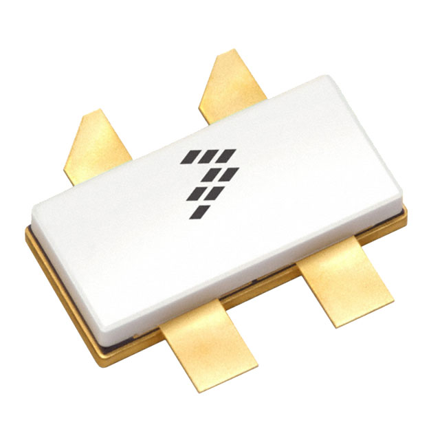
NI--780S--4L
Features
High terminal impedances for optimal broadband performance
Advanced high performance in--package Doherty
Able to withstand extremely high output VSWR and broadband operating
conditions
Carrier
RFinA/VGSA 3
1 RFoutA/VDSA
RFinB/VGSB 4
2 RFoutB/VDSB
Peaking
(Top View)
Figure 1. Pin Connections
2017, 2020 NXP B.V.
RF Device Data
NXP Semiconductors
A3G18H500--04SR3
1
�Table 1. Maximum Ratings
Rating
Symbol
Value
Unit
Drain--Source Voltage
VDSS
125
Vdc
Gate--Source Voltage
VGS
–8, 0
Vdc
Operating Voltage
VDD
0 to +55
Vdc
Maximum Forward Gate Current @ TC = 25C
IGMAX
25
mA
Storage Temperature Range
Tstg
– 65 to +150
C
Case Operating Temperature Range
TC
– 55 to +150
C
TJ
– 55 to +225
C
TMAX
275
C
Operating Junction Temperature Range
Absolute Maximum Junction Temperature
(1)
Table 2. Thermal Characteristics
Characteristic
Thermal Resistance by Infrared Measurement, Active Die Surface--to--Case
Case Temperature 76C, PD = 94.2 W
Thermal Resistance by Finite Element Analysis, Junction--to--Case
Case Temperature 76C, PD = 94.2 W
Symbol
Value
Unit
RJC (IR)
0.60 (2)
C/W
RJC (FEA)
1.02 (3)
C/W
Table 3. ESD Protection Characteristics
Test Methodology
Class
Human Body Model (per JESD22--A114)
1B
Charge Device Model (per JESD22--C101)
C3
Table 4. Electrical Characteristics (TA = 25C unless otherwise noted)
Characteristic
Off
Symbol
Min
Typ
Max
Unit
—
—
Vdc
Characteristics (4)
Drain--Source Breakdown Voltage
(VGS = –8 Vdc, ID = 24.3 mAdc)
(VGS = –8 Vdc, ID = 35.1 mAdc)
Carrier
Peaking
V(BR)DSS
150
150
On Characteristics -- Side A, Carrier
Gate Threshold Voltage
(VDS = 10 Vdc, ID = 24.3 mAdc)
VGS(th)
–3.8
–3.0
–2.3
Vdc
Gate Quiescent Voltage
(VDD = 48 Vdc, ID = 200 mAdc, Measured in Functional Test)
VGSA(Q)
–3.6
–3.0
–2.3
Vdc
IGSS
–7.5
—
—
mAdc
Gate Threshold Voltage
(VDS = 10 Vdc, ID = 20 mAdc)
VGS(th)
–3.8
–3.3
–2.3
Vdc
Gate--Source Leakage Current
(VDS = 0 Vdc, VGS = –5 Vdc)
IGSS
–7.7
—
—
mAdc
Gate--Source Leakage Current
(VDS = 0 Vdc, VGS = –5 Vdc)
On Characteristics -- Side B, Peaking
1. Functional operation above 225C has not been characterized and is not implied. Operation at TMAX (275C) reduces median time to failure
by an order of magnitude; operation beyond TMAX could cause permanent damage.
2. Refer to AN1955, Thermal Measurement Methodology of RF Power Amplifiers. Go to http://www.nxp.com/RF and search for AN1955.
3. RJC (FEA) must be used for purposes related to reliability and limitations on maximum junction temperature. MTTF may be estimated by
the expression MTTF (hours) = 10[A + B/(T + 273)], where T is the junction temperature in degrees Celsius, A = –10.3 and B = 8260.
4. Each side of device measured separately.
(continued)
A3G18H500--04SR3
2
RF Device Data
NXP Semiconductors
�Table 4. Electrical Characteristics (TA = 25C unless otherwise noted) (continued)
Characteristic
Symbol
Min
Typ
Max
Unit
(1,2)
Functional Tests
(In NXP Doherty Test Fixture, 50 ohm system) VDD = 48 Vdc, IDQA = 200 mA, VGSB = –5 Vdc, Pout = 107 W Avg.,
f = 1840 MHz, Single--Carrier W--CDMA, IQ Magnitude Clipping, Input Signal PAR = 9.9 dB @ 0.01% Probability on CCDF. ACPR measured
in 3.84 MHz Channel Bandwidth @ 5 MHz Offset. [See note on correct biasing sequence.]
Power Gain
Gps
14.5
15.4
17.5
dB
Drain Efficiency
D
53.0
57.7
—
%
PAR
6.3
7.0
—
dB
ACPR
—
–33.2
–29.0
dBc
Output Peak--to--Average Ratio @ 0.01% Probability on CCDF
Adjacent Channel Power Ratio
Load Mismatch (In NXP Test Fixture, 50 ohm system) IDQA = 200 mA, VGSB = –5 Vdc, f = 1840 MHz, 12 sec(on), 10% Duty Cycle
VSWR 10:1 at 55 Vdc, 575 W Pulsed CW Output Power
(3 dB Input Overdrive from 417 W Pulsed CW Rated Power)
No Device Degradation
Typical Performance (2) (In NXP Doherty Test Fixture, 50 ohm system) VDD = 48 Vdc, IDQA = 200 mA, VGSB = –5 Vdc, 1805–1880 MHz
Bandwidth
Pout @ 3 dB Compression Point (3)
P3dB
—
537
—
W
—
–15
—
VBWres
—
200
—
MHz
Gain Flatness in 75 MHz Bandwidth @ Pout = 107 W Avg.
GF
—
0.3
—
dB
Gain Variation over Temperature
(–30C to +85C)
G
—
0.009
—
dB/C
P1dB
—
0.004
—
dB/C
AM/PM
(Maximum value measured at the P3dB compression point across
the 1805–1880 MHz bandwidth)
VBW Resonance Point
(IMD Third Order Intermodulation Inflection Point)
Output Power Variation over Temperature
(–30C to +85C)
Table 5. Ordering Information
Device
A3G18H500--04SR3
Tape and Reel Information
R3 Suffix = 250 Units, 32 mm Tape Width, 13--inch Reel
Package
NI--780S--4L
1. Part internally input matched.
2. Measurements made with device in an asymmetrical Doherty configuration.
3. P3dB = Pavg + 7.0 dB where Pavg is the average output power measured using an unclipped W--CDMA single--carrier input signal where
output PAR is compressed to 7.0 dB @ 0.01% probability on CCDF.
NOTE: Correct Biasing Sequence for GaN Depletion Mode Transistors in a Doherty Configuration
Bias ON the device
1. Set gate voltage VGSA and VGSB to –5 V.
2. Set drain voltage VDSA and VDSB to nominal supply voltage (+48 V).
3. Increase VGSA (carrier side) until IDQA current is attained.
4. Increase VGSB (peaking side) to target bias voltage.
5. Apply RF input power to desired level.
Bias OFF the device
1. Disable RF input power.
2. Adjust gate voltage VGSA and VGSB to –5 V.
3. Adjust drain voltage VDSA and VDSB to 0 V. Allow adequate time
for drain voltage to reduce to 0 V from external drain capacitors.
4. Disable VGSA and VGSB.
A3G18H500--04SR3
RF Device Data
NXP Semiconductors
3
�VGGA
C15
VDDA
A3G18H500--04S
Rev. 3
C27
C28
C8
C22
C13
C16
C1
R1
C2
C
R3
C7
Z1
C6
C5
P
C25 C26
C21
CUT OUT AREA
C12
C18
C20
C19
C4
R2
C3
C10
C17
C23 C24
C11
C30
C29
D96809
VGGB
C9
VDDB
C14
Figure 2. A3G18H500--04SR3 Test Circuit Component Layout
Table 6. A3G18H500--04SR3 Test Circuit Component Designations and Values
Part
Description
Part Number
Manufacturer
C1, C2
10 pF Chip Capacitor
GQM2195C2E100JB12
Murata
C3, C16, C17
10 pF Chip Capacitor
ATC100B100GT500XT
ATC
C4, C19
15 pF Chip Capacitor
GQM2195C2E150JB12
Murata
C5
0.9 pF Chip Capacitor
GQM2195C2ER90BB12
Murata
C6
0.8 pF Chip Capacitor
GQM2195C2ER80BB12
Murata
C7, C21
0.6 pF Chip Capacitor
GQM2195C2ER60BB12
Murata
C8, C9
470 F, 63 V Electrolytic Capacitor
MCGPR63V477M13X26--RH
Multicomp
C10, C11, C12, C13, C22,
C23, C24, C25, C26
10 F Chip Capacitor
C3225X7S1H106K
TDK
C14, C15, C27, C28, C29, C30
10 F Chip Capacitor
C5750X7S2A106M
TDK
C18
3 pF Chip Capacitor
ATC100B3R0BT500XT
ATC
C20
1.3 pF Chip Capacitor
GQM2195C2E1R3BB12
Murata
R1, R2
3.3 1/4 W Chip Resistor
CRCW08053R30FKEA
Vishay
R3
50 8 W Termination Chip Resistor
C8A50Z4A
Anaren
Z1
1800–2200 MHz Band, 90, 2 dB Directional Coupler
X3C20F1--02S
Anaren
PCB
Rogers RO4350B, 0.020, r = 3.66
D96809
MTL
A3G18H500--04SR3
4
RF Device Data
NXP Semiconductors
�Gps, POWER GAIN (dB)
16.0
59
58
D
15.8
15.6
57
56
Gps
15.4
15.2
ACPR
15.0
Input Signal PAR = 9.9 dB @ 0.01% Probability on CCDF
1780
1800
1820
1840
–32
–2.6
–34
PARC
14.4
1760
–2.4
–33
14.8
14.6
–31
1860
1880
1900
–35
ACPR (dBc)
VDD = 48 Vdc, Pout = 107 W (Avg.), IDQA = 200 mA, VGSB = –5 Vdc
16.2 Single--Carrier W--CDMA, 3.84 MHz Channel Bandwidth
–36
1920
–2.8
–3.0
–3.2
PARC (dB)
60
16.4
D, DRAIN
EFFICIENCY (%)
TYPICAL CHARACTERISTICS — 1805–1880 MHz
–3.4
f, FREQUENCY (MHz)
IMD, INTERMODULATION DISTORTION (dBc)
Figure 3. Single--Carrier Output Peak--to--Average Ratio Compression
(PARC) Broadband Performance @ Pout = 107 Watts Avg.
–10
VDD = 48 Vdc, Pout = 10 W (PEP), IDQA = 200 mA
VGSB = –5 Vdc, Two--Tone Measurements
–20 (f1 + f2)/2 = Center Frequency of 1840 MHz
IM3--U
–30
IM3--L
IM5--U
–40
IM5--L
IM7--L
IM7--U
–50
–60
1
500
100
10
TWO--TONE SPACING (MHz)
16.5
0
16.0
15.5
15.0
14.5
14.0
VDD = 48 Vdc, IDQA = 200 mA, VGSB = –5 Vdc, f = 1840 MHz
Single--Carrier W--CDMA, 3.84 MHz Channel Bandwidth
–1
–2
–1 dB = 51.4 W
Gps
–5
20
PARC
Input Signal PAR = 9.9 dB @ 0.01% Probability on CCDF
60
–20
40
–3 dB = 108.0 W
40
70
50
ACPR
–2 dB = 82.0 W
–4
–15
60
D
–3
80
80
100
120
–25
–30
ACPR (dBc)
1
D DRAIN EFFICIENCY (%)
17.0
OUTPUT COMPRESSION AT 0.01%
PROBABILITY ON CCDF (dB)
Gps, POWER GAIN (dB)
Figure 4. Intermodulation Distortion Products
versus Two--Tone Spacing
–35
30
–40
20
140
–45
Pout, OUTPUT POWER (WATTS)
Figure 5. Output Peak--to--Average Ratio
Compression (PARC) versus Output Power
A3G18H500--04SR3
RF Device Data
NXP Semiconductors
5
�TYPICAL CHARACTERISTICS — 1805–1880 MHz
Gps, POWER GAIN (dB)
18
16
0
55
–10
45
1840 MHz
1805
MHz
14
ACPR
35
1880 MHz
1840 MHz
1805 MHz
D
10
1880 MHz
1805 MHz
1840 MHz
1880 MHz
12
8
65
15
Input Signal PAR = 9.9 dB @ 0.01% Probability on CCDF
1
25
10
100
5
500
–20
–30
–40
ACPR (dBc)
VDD = 48 Vdc, IDQA = 200 mA, VGSB = –5 Vdc
Single--Carrier W--CDMA
3.84 MHz Channel Bandwidth
Gps
D, DRAIN EFFICIENCY (%)
20
–50
–60
Pout, OUTPUT POWER (WATTS) AVG.
Figure 6. Single--Carrier W--CDMA Power Gain, Drain
Efficiency and ACPR versus Output Power
24
GAIN (dB)
VDD = 48 Vdc
Pin = 0 dBm
21 I
DQA = 200 mA
VGSB = –5 Vdc
18
Gain
15
12
9
6
1350
1450
1550
1650
1750
1850
1950
2050
2150
f, FREQUENCY (MHz)
Figure 7. Broadband Frequency Response
A3G18H500--04SR3
6
RF Device Data
NXP Semiconductors
�Table 7. Carrier Side Load Pull Performance — Maximum Power Tuning
VDD = 48 Vdc, IDQA = 250 mA, Pulsed CW, 10 sec(on), 10% Duty Cycle
Max Output Power
P1dB
f
(MHz)
Zsource
()
Zin
()
1805
2.56 – j6.80
2.88 + j6.46
1840
3.18 – j7.25
3.29 + j6.72
1880
3.88 – j7.65
3.69 + j6.85
Zload
()
(1)
Gain (dB)
(dBm)
(W)
D
(%)
AM/PM
()
4.22 – j7.66
17.9
53.3
215
60.6
–9
4.33 – j8.32
17.8
53.2
210
58.6
–9
4.43 – j8.45
17.8
53.0
201
58.1
–9
Max Output Power
P3dB
f
(MHz)
Zsource
()
Zin
()
Zload (2)
()
Gain (dB)
(dBm)
(W)
D
(%)
AM/PM
()
1805
2.56 – j6.80
2.63 + j6.74
5.40 – j8.08
16.2
54.2
265
65.1
–11
1840
3.18 – j7.25
3.01 + j7.11
5.30 – j8.38
16.2
54.1
256
63.9
–12
1880
3.88 – j7.65
3.52 + j7.35
5.88 – j9.20
16.2
54.0
251
62.5
–12
(1) Load impedance for optimum P1dB power.
(2) Load impedance for optimum P3dB power.
Zsource = Measured impedance presented to the input of the device at the package reference plane.
Zin
= Impedance as measured from gate contact to ground.
Zload = Measured impedance presented to the output of the device at the package reference plane.
Table 8. Carrier Side Load Pull Performance — Maximum Efficiency Tuning
VDD = 48 Vdc, IDQA = 250 mA, Pulsed CW, 10 sec(on), 10% Duty Cycle
Max Drain Efficiency
P1dB
f
(MHz)
Zsource
()
Zin
()
Zload (1)
()
Gain (dB)
(dBm)
(W)
D
(%)
AM/PM
()
1805
2.56 – j6.80
2.52 + j6.98
3.66 – j4.40
19.4
51.8
151
71.3
–23
1840
3.18 – j7.25
2.81 + j7.53
3.39 – j4.12
19.6
51.0
126
70.5
–26
1880
3.88 – j7.65
3.38 + j7.76
3.61 – j4.65
19.5
51.1
130
68.1
–25
Max Drain Efficiency
P3dB
Gain (dB)
(dBm)
(W)
D
(%)
AM/PM
()
3.93 – j4.40
17.5
52.6
181
75.4
–29
2.63 + j7.72
4.03 – j4.47
17.6
52.4
175
74.3
–29
3.25 + j8.11
4.53 – j5.02
17.7
52.5
176
72.2
–27
f
(MHz)
Zsource
()
Zin
()
1805
2.56 – j6.80
2.23 + j7.22
1840
3.18 – j7.25
1880
3.88 – j7.65
Zload
()
(2)
(1) Load impedance for optimum P1dB efficiency.
(2) Load impedance for optimum P3dB efficiency.
Zsource = Measured impedance presented to the input of the device at the package reference plane.
Zin
= Impedance as measured from gate contact to ground.
Zload = Measured impedance presented to the output of the device at the package reference plane.
Input Load Pull
Tuner and Test
Circuit
Output Load Pull
Tuner and Test
Circuit
Device
Under
Test
Zsource Zin
Zload
A3G18H500--04SR3
RF Device Data
NXP Semiconductors
7
�P1dB – TYPICAL CARRIER SIDE LOAD PULL CONTOURS — 1840 MHz
–2
–2
49
54
50
–4
50.5
E
IMAGINARY ()
IMAGINARY ()
–4
49.5
51
–6
51.5
52
–8
P
E
70
–6
56
68
–8
52.5
58
66
64
P
62
60
53
–10
4
2
6
REAL ()
8
–10
10
–2
21
–24
–22
20.5
–4
E
20
–6
19.5
19
–8
P
17
–10
IMAGINARY ()
IMAGINARY ()
–4
2
17.5
4
E
8
10
–20
–18
–16
–14
–6
–12
–10
–8
18.5
6
REAL ()
Figure 9. P1dB Load Pull Efficiency Contours (%)
Figure 8. P1dB Load Pull Output Power Contours (dBm)
–2
4
2
P
–8
18
6
REAL ()
8
10
Figure 10. P1dB Load Pull Gain Contours (dB)
NOTE:
–10
4
2
6
REAL ()
8
10
Figure 11. P1dB Load Pull AM/PM Contours ()
P
= Maximum Output Power
E
= Maximum Drain Efficiency
Gain
Drain Efficiency
Linearity
Output Power
A3G18H500--04SR3
8
RF Device Data
NXP Semiconductors
�P3dB – TYPICAL CARRIER SIDE LOAD PULL CONTOURS — 1840 MHz
–2
IMAGINARY ()
–4
51.5
52
53
–6
52.5
53.5
–8
–10
4
6
REAL ()
8
–10
10
Figure 12. P3dB Load Pull Output Power Contours (dBm)
–2
P
4
2
6
REAL ()
–2
–6
17.5
17
–8
P
15
–10
IMAGINARY ()
IMAGINARY ()
–4
18
2
15.5
4
64
8
10
–28
–26
–24
18.5
E
62
60
Figure 13. P3dB Load Pull Efficiency Contours (%)
19
–4
68
66
58
53.5
70
–6
54
2
72
E
–8
P
53
74
–4
52.5
E
IMAGINARY ()
50
–2
51
50.5
E
–22
–20
–6
–18
–12
–8
–16
–14
P
16.5
16
6
REAL ()
8
10
Figure 14. P3dB Load Pull Gain Contours (dB)
NOTE:
–10
4
2
6
REAL ()
8
10
Figure 15. P3dB Load Pull AM/PM Contours ()
P
= Maximum Output Power
E
= Maximum Drain Efficiency
Gain
Drain Efficiency
Linearity
Output Power
A3G18H500--04SR3
RF Device Data
NXP Semiconductors
9
�Table 9. Peaking Side Load Pull Performance — Maximum Power Tuning
VDD = 48 Vdc, VGSB = 3.1 Vdc, Pulsed CW, 10 sec(on), 10% Duty Cycle
Max Output Power
P1dB
f
(MHz)
Zsource
()
Zin
()
1805
1.66 – j6.38
1.51 + j6.91
1840
2.64 – j7.07
2.11 + j7.34
1880
2.30 – j7.54
2.13 + j7.92
Zload
()
(1)
Gain (dB)
(dBm)
(W)
D
(%)
AM/PM
()
1.79 – j4.63
17.7
54.8
302
54.5
–13
2.06 – j4.97
17.8
54.7
297
54.3
–13
2.01 – j5.25
17.8
54.6
292
53.2
–13
Max Output Power
P3dB
f
(MHz)
Zsource
()
Zin
()
Zload (2)
()
Gain (dB)
(dBm)
(W)
D
(%)
AM/PM
()
1805
1.66 – j6.38
1.37 + j6.95
2.61 – j5.42
16.0
56.0
398
58.7
–13
1840
2.64 – j7.07
2.02 + j7.47
2.86 – j5.78
15.9
55.8
378
56.4
–13
1880
2.30 – j7.54
2.02 + j8.07
2.87 – j5.92
16.1
55.6
365
56.8
–13
(1) Load impedance for optimum P1dB power.
(2) Load impedance for optimum P3dB power.
Zsource = Measured impedance presented to the input of the device at the package reference plane.
Zin
= Impedance as measured from gate contact to ground.
Zload = Measured impedance presented to the output of the device at the package reference plane.
Table 10. Peaking Side Load Pull Performance — Maximum Efficiency Tuning
VDD = 48 Vdc, VGSB = 3.1 Vdc, Pulsed CW, 10 sec(on), 10% Duty Cycle
Max Drain Efficiency
P1dB
f
(MHz)
Zsource
()
Zin
()
Zload (1)
()
Gain (dB)
(dBm)
(W)
D
(%)
AM/PM
()
1805
1.66 – j6.38
1.46 + j7.24
1.79 – j3.09
19.3
53.1
203
63.1
–25
1840
2.64 – j7.07
2.04 + j7.76
2.02 – j3.16
19.3
53.0
200
63.8
–25
1880
2.30 – j7.54
2.06 + j8.33
2.04 – j3.54
19.5
53.1
203
62.0
–24
Max Drain Efficiency
P3dB
Gain (dB)
(dBm)
(W)
D
(%)
AM/PM
()
2.15 – j2.96
17.7
53.9
247
69.4
–32
1.93 + j8.02
2.37 – j3.17
17.6
54.1
256
68.9
–30
2.01 + j8.60
2.52 – j3.41
17.9
54.0
250
67.1
–30
f
(MHz)
Zsource
()
Zin
()
1805
1.66 – j6.38
1.38 + j7.43
1840
2.64 – j7.07
1880
2.30 – j7.54
Zload
()
(2)
(1) Load impedance for optimum P1dB efficiency.
(2) Load impedance for optimum P3dB efficiency.
Zsource = Measured impedance presented to the input of the device at the package reference plane.
Zin
= Impedance as measured from gate contact to ground.
Zload = Measured impedance presented to the output of the device at the package reference plane.
Input Load Pull
Tuner and Test
Circuit
Output Load Pull
Tuner and Test
Circuit
Device
Under
Test
Zsource Zin
Zload
A3G18H500--04SR3
10
RF Device Data
NXP Semiconductors
�P1dB – TYPICAL PEAKING SIDE LOAD PULL CONTOURS — 1840 MHz
–2
–2
50.5
48
51
E
–3
52
–4
52.5
53
P
–5
53.5
–6
IMAGINARY ()
IMAGINARY ()
50
51.5
–3
54.5
3
REAL ()
4
–6
5
Figure 16. P1dB Load Pull Output Power Contours (dBm)
–2
19
P
–5
17.5
2
3
REAL ()
4
5
–26
–24
–22
E
–20
–18
–4
–16
–14
–5
18.5
17
–28
–3
20
19.5
1
56
2
1
–2
IMAGINARY ()
IMAGINARY ()
E
–4
–6
P
54
58
Figure 17. P1dB Load Pull Efficiency Contours (%)
20.5
16.5
60
–5
53.5
2
–3
52
–4
54
54
1
E
62
P
–12
18
3
REAL ()
4
5
Figure 18. P1dB Load Pull Gain Contours (dB)
NOTE:
–6
2
1
3
REAL ()
4
5
Figure 19. P1dB Load Pull AM/PM Contours ()
P
= Maximum Output Power
E
= Maximum Drain Efficiency
Gain
Drain Efficiency
Linearity
Output Power
A3G18H500--04SR3
RF Device Data
NXP Semiconductors
11
�P3dB – TYPICAL PEAKING SIDE LOAD PULL CONTOURS — 1840 MHz
52
IMAGINARY ()
–3
–2
53
52.5
–3
54
E
–4
54
54.5
–5
54.5
55
P
–6
55
–7
1
3
REAL ()
60
4
5
6
–4
17
P
–7
1
2
16.5
4
5
6
Figure 22. P3dB Load Pull Gain Contours (dB)
NOTE:
4
5
6
–26
–24
–22
E
–20
–4
–18
–5
–16
–12
–6
16
3
REAL ()
3
REAL ()
–28
–3
17.5
–5
2
1
–2
IMAGINARY ()
IMAGINARY ()
E
15.5
56
P
Figure 21. P3dB Load Pull Efficiency Contours (%)
18
15
58
–5
–7
18.5
14.5
E
54
–2
–6
58
–4
Figure 20. P3dB Load Pull Output Power Contours (dBm)
–3
64
62
–6
55.5
2
66
68
53.5
IMAGINARY ()
–2
–7
2
1
P
–14
3
REAL ()
4
5
6
Figure 23. P3dB Load Pull AM/PM Contours ()
P
= Maximum Output Power
E
= Maximum Drain Efficiency
Gain
Drain Efficiency
Linearity
Output Power
A3G18H500--04SR3
12
RF Device Data
NXP Semiconductors
�P3dB LOAD PULL PERFORMANCE, CARRIER — 1800–2200 MHz
Table 11. Carrier Side Load Pull Performance — Maximum Power Tuning
VDD = 48 Vdc, IDQA = 250 mA, Pulsed CW, 10 sec(on), 10% Duty Cycle
Max Output Power
P3dB
f
(MHz)
Zsource
()
Zin
()
1800
2.56 – j6.80
2.60 + j6.70
1840
3.20 – j7.30
3.00 + j7.10
1880
3.90 – j7.70
1930
Zload
()
(1)
Gain (dB)
(dBm)
D (%)
AM/PM ()
5.40 – j8.08
16.2
54.2
65.1
–11
5.30 – j8.38
16.2
54.1
63.9
–12
3.50 + j7.40
5.88 – j9.20
16.2
54.0
62.5
–12
3.90 – j7.70
4.10 + j7.78
6.00 – j9.40
16.4
54.0
63.2
–13
1990
5.60 – j7.11
5.30 + j7.70
6.60 – j9.80
16.6
54.0
64.0
–13
2110
7.80 – j5.70
7.10 + j5.70
6.50 – j10.8
16.5
53.9
64.2
–15
2200
7.50 – j1.70
6.30 + j2.90
7.04 – j12.0
16.2
53.8
59.4
–15
(1) Load impedance for optimum P3dB power.
Zsource = Measured impedance presented to the input of the device at the package reference plane.
Zin
= Impedance as measured from gate contact to ground.
Zload = Measured impedance presented to the output of the device at the package reference plane.
Table 12. Carrier Side Load Pull Performance — Maximum Efficiency Tuning
VDD = 48 Vdc, IDQA = 250 mA, Pulsed CW, 10 sec(on), 10% Duty Cycle
Max Drain Efficiency
P3dB
f
(MHz)
Zsource
()
Zin
()
Zload (1)
()
Gain (dB)
(dBm)
D (%)
AM/PM ()
1800
2.56 – j6.80
2.20 + j7.20
3.93 – j4.40
17.5
52.6
75.4
–29
1840
3.20 – j7.30
2.60 + j7.70
4.00 – j4.50
17.6
52.4
74.3
–29
1880
3.90 – j7.70
3.30 + j8.10
4.50 – j5.00
17.7
52.5
72.2
–27
1930
3.90 – j7.70
3.90 + j8.70
4.30 – j5.30
17.7
52.4
71.7
–29
1990
5.60 – j7.11
5.38 + j8.80
4.46 – j5.90
17.8
52.4
72.7
–27
2110
7.80 – j5.70
8.20 + j6.00
5.10 – j7.40
17.7
53.0
72.9
–26
2200
7.50 – j1.70
6.80 + j2.30
5.60 – j8.40
17.5
53.0
68.5
–24
(1) Load impedance for optimum P3dB efficiency.
Zsource = Measured impedance presented to the input of the device at the package reference plane.
Zin
= Impedance as measured from gate contact to ground.
Zload = Measured impedance presented to the output of the device at the package reference plane.
Input Load Pull
Tuner and Test
Circuit
Output Load Pull
Tuner and Test
Circuit
Device
Under
Test
Zsource Zin
Zload
A3G18H500--04SR3
RF Device Data
NXP Semiconductors
13
�P3dB LOAD PULL PERFORMANCE, PEAKING — 1800–2200 MHz
Table 13. Peaking Side Load Pull Performance — Maximum Power Tuning
VDD = 48 Vdc, IDQB = 350 mA, Pulsed CW, 10 sec(on), 10% Duty Cycle
Max Output Power
P3dB
f
(MHz)
Zsource
()
Zin
()
1800
2.56 – j6.80
2.20 + j6.30
1880
2.80 – j6.90
2.83 + j7.00
1930
3.00 – j7.16
1990
Zload
()
(1)
Gain (dB)
(dBm)
D (%)
AM/PM ()
2.90 – j5.90
15.6
55.7
62.9
–7
2.90 – j6.10
16.1
55.5
62.8
–9
3.50 + j7.00
3.53 – j7.50
15.7
55.5
57.1
–7
4.50 – j7.10
4.20 + j6.90
3.10 – j6.93
16.2
55.6
61.4
–9
2110
4.80 – j4.70
4.50 + j4.80
3.00 – j7.60
16.5
55.7
61.3
–10
2200
4.20 – j3.00
3.01 + j3.70
3.10 – j8.20
16.5
55.6
59.6
–12
(1) Load impedance for optimum P3dB power.
Zsource = Measured impedance presented to the input of the device at the package reference plane.
Zin
= Impedance as measured from gate contact to ground.
Zload = Measured impedance presented to the output of the device at the package reference plane.
Table 14. Peaking Side Load Pull Performance — Maximum Efficiency Tuning
VDD = 48 Vdc, IDQB = 350 mA, Pulsed CW, 10 sec(on), 10% Duty Cycle
Max Drain Efficiency
P3dB
f
(MHz)
Zsource
()
Zin
()
Zload (1)
()
Gain (dB)
(dBm)
D (%)
AM/PM ()
1800
2.56 – j6.80
1.99 + j6.80
2.30 – j3.50
17.2
54.1
73.7
–26
1880
2.80 – j6.90
2.80 + j7.60
2.40 – j4.20
17.5
54.1
70.3
–26
1930
3.00 – j7.16
3.80 + j7.80
2.80 – j4.40
17.8
54.2
69.7
–25
1990
4.50 – j7.10
4.90 + j7.50
2.40 – j4.60
17.9
54.1
70.7
–27
2110
4.80 – j4.70
5.00 + j3.80
2.30 – j5.30
18.4
54.2
71.3
–30
2200
4.20 – j3.00
2.60 + j3.30
2.60 – j6.10
18.5
54.5
68.8
–28
(1) Load impedance for optimum P3dB efficiency.
Zsource = Measured impedance presented to the input of the device at the package reference plane.
Zin
= Impedance as measured from gate contact to ground.
Zload = Measured impedance presented to the output of the device at the package reference plane.
Input Load Pull
Tuner and Test
Circuit
Output Load Pull
Tuner and Test
Circuit
Device
Under
Test
Zsource Zin
Zload
A3G18H500--04SR3
14
RF Device Data
NXP Semiconductors
�PACKAGE INFORMATION
A3G18H500--04SR3
RF Device Data
NXP Semiconductors
15
�A3G18H500--04SR3
16
RF Device Data
NXP Semiconductors
�PRODUCT DOCUMENTATION, SOFTWARE AND TOOLS
Refer to the following resources to aid your design process.
Application Notes
AN1908: Solder Reflow Attach Method for High Power RF Devices in Air Cavity Packages
AN1955: Thermal Measurement Methodology of RF Power Amplifiers
Software
.s2p File
Development Tools
Printed Circuit Boards
REVISION HISTORY
The following table summarizes revisions to this document.
Revision
Date
Description
0
May 2017
Initial release of data sheet
1
Aug. 2020
Changed upper frequency range from 1880 MHz to 2200 MHz to highlight part performance up to
2200 MHz, p. 1
Biasing sequence note: updated to reflect latest biasing sequence recommendations, p. 3
Tables 11–14, Load Pull Performance: added Carrier Side and Peaking Side load pull performance tables
showing P3dB performance across the 1800--2200 MHz band, pp. 13–14
A3G18H500--04SR3
RF Device Data
NXP Semiconductors
17
�How to Reach Us:
Home Page:
nxp.com
Web Support:
nxp.com/support
Information in this document is provided solely to enable system and software
implementers to use NXP products. There are no express or implied copyright licenses
granted hereunder to design or fabricate any integrated circuits based on the information
in this document. NXP reserves the right to make changes without further notice to any
products herein.
NXP makes no warranty, representation, or guarantee regarding the suitability of its
products for any particular purpose, nor does NXP assume any liability arising out of the
application or use of any product or circuit, and specifically disclaims any and all liability,
including without limitation consequential or incidental damages. “Typical” parameters
that may be provided in NXP data sheets and/or specifications can and do vary in
different applications, and actual performance may vary over time. All operating
parameters, including “typicals,” must be validated for each customer application by
customer’s technical experts. NXP does not convey any license under its patent rights
nor the rights of others. NXP sells products pursuant to standard terms and conditions of
sale, which can be found at the following address: nxp.com/SalesTermsandConditions.
NXP, the NXP logo, and Airfast are trademarks of NXP B.V. All other product or service
names are the property of their respective owners.
E 2017, 2020 NXP B.V.
A3G18H500--04SR3
Document Number: A3G18H500--04S
Rev. 1, 08/2020
18
RF Device Data
NXP Semiconductors
�