NXP Semiconductors
Technical Data
Document Number: AFT20S015N
Rev. 2, 04/2020
RF Power LDMOS Transistors
N--Channel Enhancement--Mode Lateral MOSFETs
These 1.5 W RF power LDMOS transistors are designed for cellular base
station applications covering the frequency range of 1805 to 2700 MHz.
AFT20S015N
AFT20S015GN
2100 MHz
Typical Single--Carrier W--CDMA Performance: VDD = 28 Vdc,
IDQ = 132 mA, Pout = 1.5 W Avg., Input Signal PAR = 9.9 dB @ 0.01%
Probability on CCDF.
Frequency
Gps
(dB)
D
(%)
Output PAR
(dB)
ACPR
(dBc)
1805–2700 MHz, 1.5 W AVG., 28 V
AIRFAST RF POWER LDMOS
TRANSISTORS
IRL
(dB)
2110 MHz
17.5
22.0
8.9
--43.0
--11
2140 MHz
17.6
22.0
9.0
--44.0
--12
2170 MHz
17.6
22.0
9.1
--44.0
--14
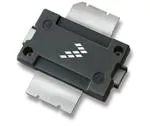
TO--270--2
PLASTIC
AFT20S015N
1800 MHz
Typical Single--Carrier W--CDMA Performance: VDD = 28 Vdc,
IDQ = 132 mA, Pout = 1.5 W Avg., Input Signal PAR = 9.9 dB @ 0.01%
Probability on CCDF.
Frequency
Gps
(dB)
D
(%)
Output PAR
(dB)
ACPR
(dBc)
IRL
(dB)
1805 MHz
18.0
21.0
9.2
--42.0
--11
1840 MHz
18.1
22.0
9.2
--44.0
--10
1880 MHz
18.0
22.0
9.1
--45.0
--10
TO--270--2 GULL
PLASTIC
AFT20S015GN
2600 MHz
Typical Single--Carrier W--CDMA Performance: VDD = 28 Vdc,
IDQ = 132 mA, Pout = 2.1 W Avg., Input Signal PAR = 9.9 dB @ 0.01%
Probability on CCDF.
Frequency
Gps
(dB)
D
(%)
Output PAR
(dB)
ACPR
(dBc)
IRL
(dB)
2300 MHz
15.7
23.0
9.0
--45.0
--6
2400 MHz
16.0
23.0
8.8
--44.0
--7
2500 MHz
15.8
23.0
8.6
--43.0
--6
2600 MHz
15.8
21.0
8.5
--43.0
--7
2700 MHz
15.5
20.0
8.4
--42.0
--8
RFin/VGS
RFout/VDS
(Top View)
Note: The backside of the package is the
source terminal for the transistor.
Figure 1. Pin Connections
Features
Greater negative gate--source voltage range for improved Class C
operation
Designed for digital predistortion error correction systems
Optimized for Doherty applications
2013, 2020 NXP B.V.
RF Device Data
NXP Semiconductors
AFT20S015N AFT20S015GN
1
�Table 1. Maximum Ratings
Symbol
Value
Unit
Drain--Source Voltage
Rating
VDSS
--0.5, +65
Vdc
Gate--Source Voltage
VGS
--6.0, +10
Vdc
Operating Voltage
VDD
32, +0
Vdc
Storage Temperature Range
Tstg
--65 to +150
C
TC
--40 to +150
C
Case Operating Temperature Range
Operating Junction Temperature Range
(1,2)
CW Operation @ TC = 25C
Derate above 25C
TJ
--40 to +225
C
CW
11
0.1
W
W/C
Symbol
Value (2,3)
Unit
RJC
4.2
C/W
Table 2. Thermal Characteristics
Characteristic
Thermal Resistance, Junction to Case
Case Temperature 77C, 1.5 W CW, 28 Vdc, IDQ = 132 mA, 2140 MHz
Table 3. ESD Protection Characteristics
Test Methodology
Class
Human Body Model (per JESD22--A114)
1C
Machine Model (per EIA/JESD22--A115)
A
Charge Device Model (per JESD22--C101)
IV
Table 4. Moisture Sensitivity Level
Test Methodology
Per JESD22--A113, IPC/JEDEC J--STD--020
Rating
Package Peak Temperature
Unit
3
260
C
Table 5. Electrical Characteristics (TA = 25C unless otherwise noted)
Symbol
Min
Typ
Max
Unit
Zero Gate Voltage Drain Leakage Current
(VDS = 65 Vdc, VGS = 0 Vdc)
IDSS
—
—
10
Adc
Zero Gate Voltage Drain Leakage Current
(VDS = 28 Vdc, VGS = 0 Vdc)
IDSS
—
—
1
Adc
Gate--Source Leakage Current
(VGS = 5 Vdc, VDS = 0 Vdc)
IGSS
—
—
1
Adc
Gate Threshold Voltage
(VDS = 10 Vdc, ID = 17.6 Adc)
VGS(th)
1.5
2.0
2.5
Vdc
Gate Quiescent Voltage
(VDD = 28 Vdc, ID = 132 mAdc, Measured in Functional Test)
VGS(Q)
2.4
3.0
3.4
Vdc
Drain--Source On--Voltage
(VGS = 10 Vdc, ID = 176 Adc)
VDS(on)
0.1
0.2
0.3
Vdc
Characteristic
Off Characteristics
On Characteristics
1. Continuous use at maximum temperature will affect MTTF.
2. MTTF calculator available at http://www.nxp.com.
3. Refer to AN1955, Thermal Measurement Methodology of RF Power Amplifiers. Go to http://www.nxp.com/RF and search for AN1955.
(continued)
AFT20S015N AFT20S015GN
2
RF Device Data
NXP Semiconductors
�Table 5. Electrical Characteristics (TA = 25C unless otherwise noted) (continued)
Characteristic
Symbol
Min
Typ
Max
Unit
(1,2)
Functional Tests
(In NXP Test Fixture, 50 ohm system) VDD = 28 Vdc, IDQ = 132 mA, Pout = 1.5 W Avg., f = 2170 MHz, Single--Carrier
W--CDMA, IQ Magnitude Clipping, Input Signal PAR = 9.9 dB @ 0.01% Probability on CCDF. ACPR measured in 3.84 MHz Channel
Bandwidth @ 5 MHz Offset.
Power Gain
Gps
16.0
17.6
19.0
dB
Drain Efficiency
D
20.0
22.0
—
%
PAR
8.6
9.1
—
dB
ACPR
—
--44.0
--41.0
dBc
IRL
—
--14
--9
dB
Output Peak--to--Average Ratio @ 0.01% Probability on CCDF
Adjacent Channel Power Ratio
Input Return Loss
Load Mismatch (In NXP Test Fixture, 50 ohm system) IDQ = 132 mA, f = 2140 MHz
VSWR 10:1 at 32 Vdc, 14 W CW (3) Output Power
(3 dB Input Overdrive from 12 W CW (3) Rated Power)
No Device Degradation
Typical Performance (In NXP Test Fixture, 50 ohm system) VDD = 28 Vdc, IDQ = 132 mA, 2110--2170 MHz Bandwidth
P1dB
—
16.2 (3,4)
—
W
—
--16
—
VBWres
—
170
—
MHz
Gain Flatness in 60 MHz Bandwidth @ Pout = 1.5 W Avg.
GF
—
0.05
—
dB
Gain Variation over Temperature
(--30C to +85C)
G
—
0.01
—
dB/C
P1dB
—
0.004
—
dB/C
Pout @ 1 dB Compression Point, CW
AM/PM
(Maximum value measured at the P3dB compression point across
the 2110--2170 MHz frequency range.)
VBW Resonance Point
(IMD Third Order Intermodulation Inflection Point)
Output Power Variation over Temperature
(--30C to +85C) (3)
Table 6. Ordering Information
Device
AFT20S015NR1
AFT20S015GNR1
Tape and Reel Information
R1 Suffix = 500 Units, 24 mm Tape Width, 13--inch Reel
Package
TO--270--2
TO--270G--2
1. Part internally matched on input.
2. Measurements made with device in straight lead configuration, before any lead forming operation is applied. Lead forming is used for gull
wing (GN) parts.
3. Exceeds recommended operating conditions. See CW operation data in Maximum Ratings table.
4. Calculated from load pull P3dB measurements.
AFT20S015N AFT20S015GN
RF Device Data
NXP Semiconductors
3
�C15
C27
C9
D47530
VGS
C19
C21
VDD
C7
C13
C23
C5*
C11
C25
C17
C2*
R1
R2
C14
C12
C6*
C18
C26
C24
C8
VGS
C20
C10
C4*
C3
CUT OUT AREA
C1*
VDD
C22
AFT20S015N
Rev. 2
C28
C16
*C1, C2, C4, C5 and C6 are mounted vertically.
Note: NXP has begun the transition of marking printed circuit boards (PCBs) with the NXP exception logo. PCBs may have either Freescale
or NXP markings during the transition period. These changes will have no impact on form, fit or function of the current product.
Figure 2. AFT20S015N Test Circuit Component Layout — 2110--2170 MHz
Table 7. AFT20S015N Test Circuit Component Designations and Values — 2110--2170 MHz
Part
Description
Part Number
Manufacturer
C1
8.2 pF Chip Capacitor
ATC100B8R2CT500XT
ATC
C2
2.4 pF Chip Capacitor
ATC800B2R4BT500XT
ATC
C3
1.7 pF Chip Capacitor
ATC100B1R7BT500XT
ATC
C4
9.1 pF Chip Capacitor
ATC100B9R1CT500XT
ATC
C5, C6
6.8 pF Chip Capacitors
ATC100B6R8CT500XT
ATC
C7, C8
240 pF Chip Capacitors
ATC100B241JT200XT
ATC
C9, C10, C21, C22
220 pF Chip Capacitors
C1812C224K5RAC--TU
Kemet
C11, C12, C23, C24
0.1 F Chip Capacitors
CDR33BX104AKWS
AVX
C13, C14, C25, C26
2.2 F Chip Capacitors
C1825C225J5RAC--TU
Kemet
C15, C16
22 F, 35 V Tantalum Capacitors
T491X226K035AT
Kemet
C17, C18, C19, C20
75 pF Chip Capacitors
ATC800B750JT500XT
ATC
C27, C28
470 F, 63 V Electrolytic Capacitors
MCGPR63V477M13X26--RH
Multicomp
R1, R2
1 Chip Resistors
CRCW12061R00FKEA
Vishay
PCB
Rogers RO4350B, 0.020, r = 3.66
D47530
MTL
AFT20S015N AFT20S015GN
4
RF Device Data
NXP Semiconductors
�Gps, POWER GAIN (dB)
17.8
22
17.7
21.5
Gps
17.6
17.5
21
IRL
17.4
17.3
PARC
--41
--9
--42
--13
--43
ACPR
17.2
--44
17.1 3.84 MHz Channel Bandwidth
Input Signal PAR = 9.9 dB @ 0.01% Probability on CCDF
17
2060 2080 2100 2120 2140 2160 2180 2200
--45
--46
2220
--17
--21
--25
--29
--0.4
--0.6
--0.8
--1
--1.2
PARC (dB)
17.9
IRL, INPUT RETURN LOSS (dB)
23
VDD = 28 Vdc, Pout = 1.5 W (Avg.)
IDQ = 132 mA, Single--Carrier W--CDMA 22.5
D
ACPR (dBc)
18
D, DRAIN
EFFICIENCY (%)
TYPICAL CHARACTERISTICS — 2110--2170 MHZ
--1.4
f, FREQUENCY (MHz)
IMD, INTERMODULATION DISTORTION (dBc)
Figure 3. Single--Carrier Output Peak--to--Average Ratio Compression
(PARC) Broadband Performance @ Pout = 1.5 Watts Avg.
--10
VDD = 28 Vdc, Pout = 10 W (PEP), IDQ = 132 mA
Two--Tone Measurements, (f1 + f2)/2 = Center
--20 Frequency of 2140 MHz
IM3--U
IM3--L
--30
IM5--U
--40
IM5--L
IM7--U
--50
IM7--L
--60
1
100
10
200
TWO--TONE SPACING (MHz)
Figure 4. Intermodulation Distortion Products
versus Two--Tone Spacing
17
16.5
16
15.5
--1
--1 dB = 1.5 W
D
--2 dB = 2.2 W
--2
--25
50
--30
40
Gps
--3
--4
60
ACPR
30
--3 dB = 3 W
20
PARC
--5 VDD = 28 Vdc, IDQ = 132 mA, f = 2140 MHz
Single--Carrier W--CDMA, 3.84 MHz Channel Bandwidth
Input Signal PAR = 9.9 dB @ 0.01% Probability on CCDF
--6
2
5
1
3
4
6
--35
--40
ACPR (dBc)
17.5
OUTPUT COMPRESSION AT 0.01%
PROBABILITY ON CCDF (dB)
Gps, POWER GAIN (dB)
18
0
D DRAIN EFFICIENCY (%)
18.5
--45
10
--50
0
--55
Pout, OUTPUT POWER (WATTS)
Figure 5. Output Peak--to--Average Ratio
Compression (PARC) versus Output Power
AFT20S015N AFT20S015GN
RF Device Data
NXP Semiconductors
5
�TYPICAL CHARACTERISTICS — 2110--2170 MHz
Gps, POWER GAIN (dB)
19
2140 MHz
18
ACPR
--10
30
2170 MHz
2140 MHz
2110 MHz
15
50
40
2110 MHz
16
0
2170 MHz
Gps
17
14
2170 MHz
D
60
20
10
3.84 MHz Channel Bandwidth, Input Signal
PAR = 9.9 dB @ 0.01% Probability on CCDF
--30
--40
--50
--60
0
20
10
1
--20
ACPR (dBc)
2140 MHz
VDD = 28 Vdc, IDQ = 132 mA
Single--Carrier W--CDMA
2110 MHz
D, DRAIN EFFICIENCY (%)
20
Pout, OUTPUT POWER (WATTS) AVG.
Figure 6. Single--Carrier W--CDMA Power Gain, Drain
Efficiency and ACPR versus Output Power
20
21
10
Gain
17
0
15
--10
13
--20
IRL
--30
11
9
1700
IRL (dB)
GAIN (dB)
19
VDD = 28 Vdc
Pin = 0 dBm
IDQ = 132 mA
1800
1900
2000
2100
2200
2300
2400
--40
2500
f, FREQUENCY (MHz)
Figure 7. Broadband Frequency Response
AFT20S015N AFT20S015GN
6
RF Device Data
NXP Semiconductors
�ALTERNATE CHARACTERIZATION — 1805--1880 MHz
C16
C28
C10
D45064
VGS
C20
VDD
C8
C14
C6*
C12
C18 C22 C24
C2*
R1
R2
C15
C13
C4*
C3*
C7*
CUT OUT AREA
C1*
C26
C5*
C19 C23 C25
C27
C9
VGS
VDD
C21
C11
AFT20S015N
Rev. 2
C29
C17
*C1, C2, C3, C4, C5, C6 and C7 are mounted vertically.
Note: NXP has begun the transition of marking printed circuit boards (PCBs) with the NXP exception logo. PCBs may have either Freescale
or NXP markings during the transition period. These changes will have no impact on form, fit or function of the current product.
Figure 8. AFT20S015N Test Circuit Component Layout — 1805--1880 MHz
Table 8. AFT20S015N Test Circuit Component Designations and Values — 1805--1880 MHz
Part
Description
Part Number
Manufacturer
C1
11 pF Chip Capacitor
ATC100B11R0CT500XT
ATC
C2, C3
3.3 pF Chip Capacitors
ATC800B3R3BT500XT
ATC
C4, C5
47 pF Chip Capacitors
ATC600F47BT250XT
ATC
C6, C7
6.8 pF Chip Capacitors
ATC100B6R8CT500XT
ATC
C8, C9
240 pF Chip Capacitors
ATC100B241JT200XT
ATC
C10, C11, C22, C23
220 pF Chip Capacitors
C1812C224K5RAC--TU
Kemet
C12, C13, C24, C25
0.1 F Chip Capacitors
CDR33BX104AKWS
AVX
C14, C15, C26, C27
2.2 F, 50 V Chip Capacitors
C1825C225J5RAC--TU
Kemet
C16, C17
22 F, 35 V Tantalum Capacitors
T491X226K035AT
Kemet
C18, C19, C20, C21
75 pF Chip Capacitors
ATC800B750JT500XT
ATC
C28, C29
470 F, 63 V Electrolytic Capacitors
MCGPR63V477M13X26--RH
Multicomp
R1, R2
1 Chip Resistors
CRCW12061R00FKEA
Vishay
PCB
Rogers RO4350B, 0.020, r = 3.66
D45064
MTL
AFT20S015N AFT20S015GN
RF Device Data
NXP Semiconductors
7
�ALTERNATE CHARACTERIZATION — 1805--1880 MHz
Gps
18.2
18
ACPR
17.8
17.6
17.2
17
1760
1780
--9
--42
--9.5
--43
PARC
17.4
--41
--44
IRL
--45
1800
--46
1920
1820
1840
1860
1880
1900
--10
--10.5
--11
--11.5
--0.3
--0.4
--0.5
--0.6
--0.7
PARC (dB)
Gps, POWER GAIN (dB)
18.4
22
21
VDD = 28 Vdc, Pout = 1.5 W (Avg.)
IDQ = 132 mA, Single--Carrier W--CDMA
20
3.84 MHz Channel Bandwidth, Input Signal
PAR = 9.9 dB @ 0.01% Probability on CCDF 19
IRL, INPUT RETURN LOSS (dB)
D
18.6
D, DRAIN
EFFICIENCY (%)
23
ACPR (dBc)
19
18.8
--0.8
f, FREQUENCY (MHz)
Figure 9. Single--Carrier Output Peak--to--Average Ratio Compression
(PARC) Broadband Performance @ Pout = 1.5 Watts Avg.
18
1805 MHz
ACPR
25
--30
15
10
1880 MHz
17.9
--25
20
Gps
18.1
D
1880 MHz
30
1805 MHz
1880 MHz
1840 MHz
5
17.8 Input Signal PAR = 9.9 dB @ 0.01% Probability on CCDF
1
0.1
5
--35
--40
--45
ACPR (dBc)
1805 MHz
1840 MHz
VDD = 28 Vdc, IDQ = 132 mA
Single--Carrier W--CDMA
18.3 3.84 MHz Channel Bandwidth
1840 MHz
18.2
D, DRAIN EFFICIENCY (%)
Gps, POWER GAIN (dB)
18.4
--50
--55
0
Pout, OUTPUT POWER (WATTS) AVG.
Figure 10. Single--Carrier W--CDMA Power Gain, Drain
Efficiency and ACPR versus Output Power
0
21
Gain
--2
17
--4
15
--6
13
--8
IRL
--10
11
9
1400
IRL (dB)
GAIN (dB)
19
VDD = 28 Vdc
Pin = 0 dBm
IDQ = 132 mA
1500
1600
1700
1800
1900
2000
2100
--12
2200
f, FREQUENCY (MHz)
Figure 11. Broadband Frequency Response
AFT20S015N AFT20S015GN
8
RF Device Data
NXP Semiconductors
�ALTERNATE CHARACTERIZATION — 2300--2700 MHz
C15
C20
C9
D48048
VGS
C18 C19
C7
C13
C11
C5
C4*
C17
C2*
C1*
VDD
C21
C3*
R1
C14
C6
C12
CUT OUT AREA
R2
C8
VGS
VDD
C10
AFT20S015N 2.6 GHz
Rev. 0
C16
*C1, C2, C3 and C4 are mounted vertically.
Note: NXP has begun the transition of marking printed circuit boards (PCBs) with the NXP exception logo. PCBs may have either Freescale
or NXP markings during the transition period. These changes will have no impact on form, fit or function of the current product.
Figure 12. AFT20S015N Test Circuit Component Layout — 2300--2700 MHz
Table 9. AFT20S015N Test Circuit Component Designations and Values — 2300--2700 MHz
Part
Description
Part Number
Manufacturer
C1
4.3 pF Chip Capacitor
ATC600F4R3CT250XT
ATC
C2
1.3 pF Chip Capacitor
ATC800B1R3BT500XT
ATC
C3
8.2 pF Chip Capacitor
ATC600F8R2BT250XT
ATC
C4
6.8 pF Chip Capacitor
ATC100B6R8CT500XT
ATC
C5, C6
6.8 pF Chip Capacitors
ATC800B6R8CT500XT
ATC
C7, C8, C17
2.2 F Chip Capacitors
C3225X7R1H225KT
TDK
C9, C10, C18
220 nF Chip Capacitors
C1812C224K5RAC--TU
Kemet
C11, C12, C19
0.1 F Chip Capacitors
CDR33BX104AKWS
AVX
C13, C14, C21
2.2 F Chip Capacitors
C1825C225J5RAC--TU
Kemet
C15, C16
22 F, 35 V Tantalum Capacitors
T491X226K035AT
Kemet
C20
470 F, 63 V Electrolytic Capacitor
MCGPR63V477M13X26--RH
Multicomp
R1, R2
4.75 Chip Resistors
CRCW12064R75FKEA
Vishay
PCB
Rogers RO4350B, 0.020, r = 3.66
D48048
MTL
AFT20S015N AFT20S015GN
RF Device Data
NXP Semiconductors
9
�ALTERNATE CHARACTERIZATION — 2300--2700 MHz
19
Gps
15.5
17
Single--Carrier W--CDMA 3.84 MHz Channel
Bandwidth, Input Signal PAR = 9.9 dB @
ACPR
0.01% Probability on CCDF
15
14.5
--39
0
--41
--2
--43
14
13.5
--45
IRL
13
12.5
2200
--47
PARC
2275
2350
2425
2500
2575
2650
--6
--8
--10
--49
2800
2725
--4
--0.6
--0.8
--1
--1.2
--1.4
PARC (dB)
16
IRL, INPUT RETURN LOSS (dB)
D
16.5
Gps, POWER GAIN (dB)
25
VDD = 28 Vdc, Pout = 2.1 W (Avg.)
IDQ = 132 mA 23
21
D, DRAIN
EFFICIENCY (%)
17
ACPR (dBc)
17.5
--1.6
f, FREQUENCY (MHz)
Figure 13. Single--Carrier Output Peak--to--Average Ratio Compression
(PARC) Broadband Performance @ Pout = 2.1 Watts Avg.
2300 MHz
2500 MHz
D
2700 MHz
--25
25
--30
20
15.8
Gps
15.6
15.4
30
15
2300 MHz 2500 MHz
2700 MHz
10
2300 MHz
5
ACPR 2700 MHz
2500 MHz
Input Signal PAR = 9.9 dB @ 0.01% Probability on CCDF 0
1
5
15.2
15
0.1
--35
--40
--45
ACPR (dBc)
Gps, POWER GAIN (dB)
VDD = 28 Vdc, IDQ = 132 mA
Single--Carrier W--CDMA
16 3.84 MHz Channel Bandwidth
D, DRAIN EFFICIENCY (%)
16.2
--50
--55
Pout, OUTPUT POWER (WATTS) AVG.
Figure 14. Single--Carrier W--CDMA Power Gain, Drain
Efficiency and ACPR versus Output Power
2
21
0
GAIN (dB)
17
--2
Gain
15
--4
13
--6
IRL
11
9
2100
2250
2400
2550
2700
IRL (dB)
19
VDD = 28 Vdc
Pin = 0 dBm
IDQ = 132 mA
--8
2850
3000
3150
--10
3300
f, FREQUENCY (MHz)
Figure 15. Broadband Frequency Response
AFT20S015N AFT20S015GN
10
RF Device Data
NXP Semiconductors
�PACKAGE INFORMATION
AFT20S015N AFT20S015GN
RF Device Data
NXP Semiconductors
11
�AFT20S015N AFT20S015GN
12
RF Device Data
NXP Semiconductors
�AFT20S015N AFT20S015GN
RF Device Data
NXP Semiconductors
13
�AFT20S015N AFT20S015GN
14
RF Device Data
NXP Semiconductors
�AFT20S015N AFT20S015GN
RF Device Data
NXP Semiconductors
15
�AFT20S015N AFT20S015GN
16
RF Device Data
NXP Semiconductors
�PRODUCT DOCUMENTATION, SOFTWARE AND TOOLS
Refer to the following documents, software and tools to aid your design process.
Application Notes
AN1907: Solder Reflow Attach Method for High Power RF Devices in Plastic Packages
AN1955: Thermal Measurement Methodology of RF Power Amplifiers
AN3789: Clamping of High Power RF Transistors and RFICs in Over--Molded Plastic Packages
Software
Electromigration MTTF Calculator
RF High Power Model
.s2p File
Development Tools
Printed Circuit Boards
REVISION HISTORY
The following table summarizes revisions to this document.
Revision
Date
Description
0
Apr. 2013
Initial Release of Data Sheet
1
Nov. 2013
Upper frequency limit changed from 2690 to 2700 MHz to reflect measurement data, p. 1
Table 2, Thermal Characteristics: changed 2170 to 2140 MHz to reflect recent thermal test results, p. 2
Table 5, Electrical Characteristics, Load Mismatch: updated VSWR power levels (8 W CW to 14 W CW,
7 W CW to 12 W CW) to reflect recent characterization data test results, p. 3
Table 5, Electrical Characteristics, Typical Performance: changed P1dB from 7 W to 16.2 W based on
P3dB load pull calculations, p. 3
Figs. 2, 8, 12, Test Circuit Component Layout: added MTL number, pp. 4, 7, 9
Tables 6, 7, 8, Test Circuit Component Designations and Values: updated PCB description to reflect most
current board specifications from Rogers and added MTL part number, pp. 4, 7, 9
2
Apr. 2020
Package Outline Drawings: TO–270–2 package outline updated to Rev. R, pp. 11–13. TO–270G–2
package outline updated to Rev. D, pp. 14–16.
General updates made to align data sheet to current standard
AFT20S015N AFT20S015GN
RF Device Data
NXP Semiconductors
17
�How to Reach Us:
Home Page:
nxp.com
Web Support:
nxp.com/support
Information in this document is provided solely to enable system and software
implementers to use NXP products. There are no express or implied copyright licenses
granted hereunder to design or fabricate any integrated circuits based on the information
in this document. NXP reserves the right to make changes without further notice to any
products herein.
NXP makes no warranty, representation, or guarantee regarding the suitability of its
products for any particular purpose, nor does NXP assume any liability arising out of the
application or use of any product or circuit, and specifically disclaims any and all liability,
including without limitation consequential or incidental damages. “Typical” parameters
that may be provided in NXP data sheets and/or specifications can and do vary in
different applications, and actual performance may vary over time. All operating
parameters, including “typicals,” must be validated for each customer application by
customer’s technical experts. NXP does not convey any license under its patent rights
nor the rights of others. NXP sells products pursuant to standard terms and conditions of
sale, which can be found at the following address: nxp.com/SalesTermsandConditions.
NXP, the NXP logo, Freescale, the Freescale logo and Airfast are trademarks of
NXP B.V. All other product or service names are the property of their respective owners.
E 2013, 2020 NXP B.V.
AFT20S015N AFT20S015GN
Document Number: AFT20S015N
Rev. 2, 04/2020
18
RF Device Data
NXP Semiconductors
�