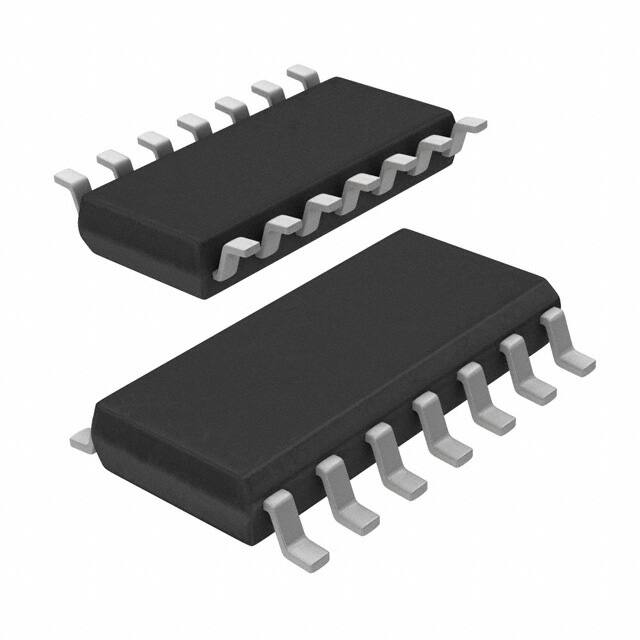
INTEGRATED CIRCUITS
AU5783
J1850/VPW transceiver with
supply control function
Preliminary specification
Supersedes data of 2000 Nov 29
�����
�����
����
�
2001 Feb 15
�Philips Semiconductors
Preliminary specification
J1850/VPW transceiver with supply control function
FEATURES
AU5783
DESCRIPTION
• Supports SAE/J1850 VPW standard for in-vehicle class B
The AU5783 is a line transceiver being primarily intended for
in-vehicle multiplex applications. It provides interfacing between a
J1850 link controller and the physical bus wire. The device supports
the SAE/J1850 VPWM standard with a nominal bus speed of
10.4 kbit/s. For data upload and download purposes the 4X
transmission mode is supported with a nominal bus speed of
41.6 kbit/s. The AU5783 provides protection against loss of ground
conditions, thus ensuring the network will be operational in case of
an electronic control unit loosing connection to ground potential. Low
power operation is supported through provision of a sleep mode with
very low power consumption. In addition an external voltage
regulator can be turned off via the AU5783 transceiver to further
reduce the overall power consumption. The voltage regulator will be
activated again upon detection of bus activity or upon a local
wake-up event.
multiplexing
• Bus speed 10.4 kbit/s nominal
• 4X transmission mode (41.6 kbit/s)
• Drive capability 32 bus nodes
• Low RFI due to output waveshape function
• Direct battery operation with protection against +40 V load dump
and 8 kV ESD
• Bus terminals proof against automotive transients up to
+100 V/–150 V and 8 kV ESD
• Power supply enable function
• Very low sleep mode power consumption
• Diagnostic loop-back mode
• Thermal overload protection
• 14-pin SOIC
ORDERING INFORMATION
TYPE NUMBER
AU5783D
PACKAGE
NAME
SO14
DESCRIPTION
TEMPERATURE
RANGE
VERSION
plastic small outline package; 14 leads; body width 3.9 mm
SOT108-1
–40 to +125°C
QUICK REFERENCE DATA
SYMBOL
PARAMETER
CONDITIONS
VBAT.op
Operating supply voltage, including low battery
operation
Tamb
Operating ambient temperature range
VBAT.ld
Battery voltage
load dump, 1s
VBOH
Bus output voltage
250 Ω < RL < 1.6 kΩ
VBI
Bus input threshold
IBAT.lp
Sleep mode supply current
tP
Propagation delay
tr
Bus output rise time
2001 Feb 15
MIN.
5.5
TYP.
12
UNIT
V
+125
°C
+40
V
6.7
8.0
V
3.4
4.2
V
90
µA
25
µs
–40
Tx to Rx
14
2
MAX.
16
µs
�Philips Semiconductors
Preliminary specification
J1850/VPW transceiver with supply control function
AU5783
BLOCK DIAGRAM
BATTERY (+12V)
BAT
VOLTAGE
TEMP.
REFERENCE
PROTECTION
R/F
Rs
TX
TX–
OUTPUT
BUFFER
BUFFER
BUS
NSTB
MODE
Rld
4X/LOOP
CONTROL
Vcc (+5V)
Rd
1.6V
LOAD
RX
VOLTAGE
Vbat
LOAD
SWITCH
REFERENCE
INH
WAKE-UP
LWAKE
CONTROL
AU5783
GND
SL01224
Figure 1. Block diagram
2001 Feb 15
3
�Philips Semiconductors
Preliminary specification
J1850/VPW transceiver with supply control function
AU5783
PINNING
Pin configuration
FUNCTIONAL DESCRIPTION
R/F
1
14
GND
GND
2
13
N.C.
4X/LOOP
3
12
BUS
NSTB
4
11
LOAD
TX
5
10
INH
RX
6
9
LWAKE
N.C.
7
8
BAT
AU5783
The AU5783 is an integrated line transceiver IC that interfaces an
SAE/J1850 protocol controller IC to the vehicle’s multiplex bus line.
It is primarily intended for automotive “Class B” multiplexing
applications in passenger cars using VPW (Variable Pulse Width)
modulated signals with a nominal transmission speed of 10.4 kbit/s.
The device provides transmit and receive capability as well as
protection to a J1850 electronic module.
A J1850 link controller feeds the transmit data stream to the
transceiver’s TX input. The AU5783 transceiver waveshapes the TX
data input signal so as to minimize electromagnetic emission. The
bus output signal features controlled rise & fall characteristic
including rounded shape. A resistance being connected to the R/F
control input sets the bus output slew rate.
The LOAD output is connected to the physical bus line via an
external load resistor Rld. The load resistor pulls the bus line to
ground potential being the default state, e.g., when no transmitter
outputs an active state. This output ensures the J1850 network will
not be affected by a potential loss of ground condition at an
individual electronic control unit.
SO14
SL01225
Figure 2. Pin configuration
The AU5783 includes a bus receiver with filter function to minimize
susceptibility against interference. The logic state of the J1850 bus
signal is indicated at the RX output being connected to the J1850
link controller.
Pin description
SYMBOL
PIN
DESCRIPTION
R/F
1
Rise/fall time control input; connect to ground
potential via a resistor
GND
2
Ground
4X/LOOP
3
Tx mode control input; low: normal mode;
high: 4X mode; float: loopback
NSTB
4
Network STandBy power control input; low:
transmit function disabled (low power modes);
high: transmit function enabled
TX
5
Transmit data input; low: transmitter passive;
high: transmitter active
RX
6
Receive data output; low: active bus condition
detected; high: otherwise
N.C.
7
Not connected
BAT
8
Battery supply input, 12V nominal
LWAKE
9
Local wake-up input, edge sensitive
INH
10
Activity indication flag (inhibit) output high side
driver; e.g., to control a voltage regulator.
Active high enables the regulator
LOAD
11
Bus load in/output
BUS
12
Bus line transmit/receive input/output, active
high side driver
N.C.
13
Not connected
GND
14
Ground
The AU5783 also provides advanced low-power modes to help
minimize ignition-off power consumption of an electronic control unit.
The bus receiver function is kept alive in the low-power modes. If an
active state is being detected on the bus line this will be indicated
via the RX output. By default the AU5783 enters the low-power
standby mode when the mode control inputs NSTB and 4X/LOOP
are not driven. A 100 kΩ pull down resistor is required on NSTB.
Ignition-off current draw can be reduced further by turning off the
voltage regulator being typically provided in an electronic control
unit. This is supported by the activity indication function of the
AU5783. In this application the activity indication flag INH will control
external devices such as a voltage regulator. To turn-off the INH flag
and thus the voltage regulator, the go to sleep command needs to
be applied to the Network Standby power control input,
e.g., NSTB = 0. The INH output is turned off after the sleep time-out
period thereby, reducing the power consumption of an electronic
control unit to an extremely low level.
The activity indication flag INH will be turned on again upon
detection of a remote wake-up condition (i.e. bus activity) or upon
detection of a local wake-up condition or a respective command
from the microcontroller. A local wake-up condition is detected
when an edge occurs at the wake-up input LWAKE. The INH flag
will also be turned on upon detection of a high input level at the
mode control input NSTB. Activation of the INH output enables
external devices, e.g., a voltage regulator. This condition will power-up
logic devices, e.g., a microcontroller in order to perform appropriate
action, e.g., activation of the AU5783 and the J1850 network.
The AU5783 contain a power on reset (POR) circuit, which is active
at low voltages. This circuit insures that if the control input NSTB is
at 0 V or floating during power up, the device will be forced into the
standby mode by the time the battery voltage rises to 4.4 V. This will
also insure that the INH pin is in the high state to turn on the local
voltage regulator. If there is a dip going below 4.4 V in battery
voltage while in the sleep mode, the device may return to the
2001 Feb 15
4
�Philips Semiconductors
Preliminary specification
J1850/VPW transceiver with supply control function
essentially disconnecting an electronic control unit from the J1850
bus line. The TX signal is internally looped back to the RX output.
standby mode if the POR is tripped. Even if the device is not in
sleep mode the INH output will turn off at some battery voltages
below 4.4 V when the internal POR circuit is active. At still lower
voltages where the POR circuit does not operate, the INH may
again pull up toward the battery level, typically with battery voltages
below approximately 3.6 V. The operation of the POR circuit can be
verified by placing the device in the sleep mode while the battery
voltage is above 4.4 V. The INH output, which is a high side driver,
should turn off when the sleep mode is entered. Next ramp the
battery voltage down to 2.0V and finally return the battery voltage to
4.4 V. When the battery supply is returned to 4.4V, the INH output
will pull high since the device enters standby mode. The actual
voltages at which the POR engages and releases will vary from part
to part. The lowest voltage at which the POR will be active is 2.6 V
and it will always release below 4.4 V.
The AU5783 only requires one power supply VBAT. Bus
transmissions can continue with battery voltage down to 5.5 V. The
bus output voltage will track 1.3V bellow the battery voltage. The
bus input voltage threshold will also follow the battery voltage going
down as shown in Figure 3. This ratio metric behavior of the input
threshold partially compensates for the reduced dominant level
transmitted during low battery operation.
The AU5783 features special robustness at its BAT and BUS pins
hence the device is well protected for applications in the automotive
environment. Specifically the BAT input is protected against 40 V
load dump and jump start condition. The BUS output is protected
against wiring fault conditions, e.g., short circuit to ground and
battery voltage as well as typical automotive transients and
electrostatic discharge. In addition, an over-temperature shutdown
function with hysteresis is incorporated which protects the device
under network fault conditions. In case of the die temperature
reaching the trip point, the AU5783 will latch-off the transceiver
function. The device is reset on the first rising edge on the TX input
after a decrease in the junction temperature.
The AU5783 provides a high-speed data transmission mode where
the bus output waveshape function is disabled. In this mode transmit
signals are output as fast as possible thus allowing higher data
rates, e.g., the so-called 4X mode with 41.6 kbit/s nominal speed.
The AU5783 also provides a loop-back mode for diagnostic
purpose, e.g., self-test of an electronic control unit. In loop-back
mode the bus transmit and receive functions are disabled thus
5.5
4.2
3.9
3.4
~
~
~
~
bus output
bus input
~
~
Bus Voltage (V)
6.7
ÈÈÈÈÈÈÈÈÈÈÈÈÈÈÈÈ
ÈÈÈÈÈÈÈÈÈÈÈÈÈÈÈÈ
ÈÈÈÈÈÈÈÈÈÈÈÈÈÈÈÈ
ÈÈÈÈÈÈÈÈÈÈÈÈÈÈÈÈ
ÈÈÈ
ÈÈÈÈÈÈÈÈÈÈÈÈÈÈÈÈ
ÈÈÈ
ÈÈÈÈÈÈÈÈÈÈÈÈÈÈÈÈ
ÈÈÈÈÈÈÈÈÈÈÈÈÈÈÈÈ
~
~
8
AU5783
1.9
5.5 5.8
7
8
16
Battery Voltage (V)
Figure 3. Bus voltage vs battery voltage
2001 Feb 15
5
SL01254
�Philips Semiconductors
Preliminary specification
J1850/VPW transceiver with supply control function
AU5783
Table 1. Control input summary
Z = Input connected to high impedance permitting it to float. Typically accomplished by turning off the output of a microcontroller.
X = Don’t care; The input may be at either logic level.
NSTB
4X/LOOP
TX
1
0
1
normal operation
active
high
low
high
1
0
0
normal operation
passive
float
bus state,
Note 2
high
1
1
1
4X transmit
active
high
low
high
1
1
0
4X transmit
passive
float
bus state,
Note 2
high
1
Z
1
loop-back
passive
float
low
high
1
Z
0
loop-back
passive
float
high
high
0 or Z
X
X
standby (default state after power on),
Note 1, Note 6
off
float
bus state,
Note 5
high
1 –> 0
X
0
go to sleep command, Note 4, Note 6
off
float
bus state,
Note 5
float, Note 3
0 or Z
X
X
sleep, Note 4, Note 6
off
float
bus state,
Note 5
float
Mode
Bus
transmitter
BUS
RX (out)
INH
NOTES:
1. After power-on, the AU5783 enters standby mode since the input pins NSTB and 4X/LOOP are assumed to be floating. In standby mode the
voltage regulator is enabled via the INH output, and therefore power is supplied to the microcontroller. When the microcontroller begins
operation it will normally set the control inputs NSTB high and 4X/LOOP to low state in order to start normal operation of the AU5783.
2. RX outputs the bus state. If the bus level is below the receiver threshold (i.e., all transmitters passive), then RX will be high. Otherwise, if the
bus level is above the receiver threshold (i.e., at least one transmitter is active), then RX will be low.
3. INH is turned off after a time-out period.
4. For entering the sleep mode (e.g., to deactivate INH), the “Go To Sleep” command needs to be applied. The “Go To Sleep” command is a
high-to-low transition on the NSTB input. When the “Go To Sleep” command is present, the INH flag is deactivated. This signal can be used
to turn-off the voltage regulator of an electronic module. After the voltage regulator is turned off the microcontroller is no longer supplied and
the NSTB input will be floating. The INH output will be set again upon detection of bus activity or occurrence of a local wake-up event.
5. In standby and sleep mode, the detection of a wake-up condition (e.g., high level on BUS) will be signalled on the output RX.
6. The NSTB pin contains a weak pull down which is active in the normal, loop-back and high-speed modes but is disabled in the sleep mode.
To insure a logic 0 input if the microcontroller’s outputs are tri-stated or the microcontroller is not powered, a 100 kΩ resistor between NSTB
and ground is suggested.
2001 Feb 15
6
�Philips Semiconductors
Preliminary specification
J1850/VPW transceiver with supply control function
AU5783
ABSOLUTE MAXIMUM RATINGS
According to the IEC 134 Absolute Maximum System.
Unless otherwise specified, operation is not guaranteed under these conditions: all voltages are referenced to pin GND; positive currents flow
into the IC.
SYMBOL
PARAMETER
CONDITIONS
VBAT
Voltage on pin BAT
VBAT.ld
Short-term supply voltage
load dump, t < 1s
VBAT.tr
Transient voltage on pin BAT and pin
LWAKE
SAE J1113 test pulses 3A and 3B,
Rwake > 9 kΩ
VB0
Bus voltage
VB1
VB.tr
VWKE
Voltage on pin LWAKE
VWKR
Voltage on pin LWAKE
VINH
MIN.
MAX.
UNIT
+34
V
+40
V
–150
+100
V
VBAT < 2 V, Rld > 1.4 kΩ
–16
+18
V
Bus voltage
VBAT > 2 V, Rld > 1.4 kΩ
–10
+18
V
Transient bus voltage
SAE J1113, test pulses 3A and 3B,
coupled via C = 1 nF; Rld > 1.4 kΩ
–150
+100
V
–0.3
≤ VBAT
V
–16
+34
V
DC voltage on pin INH
–0.3
≤ VBAT
V
VI
DC voltage on pins TX, RX, NSTB and
4X/LOOP
–0.3
7.0
V
VI,RF
DC voltage on pin R/F
–0.3
5.0
V
ESDHBM1
ESD capability of pins BAT, BUS, LOAD
and LWAKE
Human body model, direct contact
discharge, R = 1.5 kΩ, C = 100 pF,
Rld > 1.4 kΩ; Rwake > 9 kΩ
–8
+8
kV
ESDHBM2
ESD capability of all pins
Human body model, direct contact
discharge, R = 1.5 kΩ, C = 100 pF
–2
+2
kV
Ptot
Maximum power dissipation
@ Tamb = +125°C
205
mW
ΘJA
Thermal impedance
with standard test PCB
120
°C/W
Tamb
Operating ambient temperature
–40
+125
°C
Tvj
Operating junction temperature
–40
+150
°C
Tstg
Storage temperature
–40
+150
°C
2001 Feb 15
–0.3
via series resistor of Rwake > 9 kΩ
7
�Philips Semiconductors
Preliminary specification
J1850/VPW transceiver with supply control function
AU5783
DC ELECTRICAL CHARACTERISTICS
7V < VBAT < 16 V; –40 °C < Tamb < +125 °C; 250 Ω < RL < 1.6 kΩ; 1.4 kΩ < Rld < 12 kΩ;
–2V < Vbus < +9 V; NSTB = 5 V; 4X/LOOP = 5 V; Rs = 56 kΩ ± 1%; RX connected to +5 V via Rd = 3.9 kΩ; INH loaded with 100 kΩ to GND;
LWAKE connected to BAT via 10 kΩ resistor; all voltages are referenced to pin 14 (GND); positive currents flow into the IC;
typical values reflect the approximate average value at VBAT = 13 V and Tamb = 25 °C; unless otherwise specified.
SYMBOL
PARAMETER
CONDITIONS
MIN.
TYP.
MAX.
UNIT
Pin BAT & thermal shutdown
IBAT.sl
Sleep mode supply current
Note 1
90
µA
IBAT.sb
Standby mode supply current
Note 1
500
µA
IBAT.p.nl
TX = 5 V; LWAKE = 0 V,
4X/LOOP = 0 or Z
TX = 5 V; LWAKE = 0 V,
4X/LOOP = 5 V
TX = 5 V, RL = 1.38 kΩ, Note 2
3
mA
10
mA
IBAT.wl
Supply current; passive state, in normal or
loopback modes
Supply current; passive state, in high
speed mode
Supply current; weak load
25
mA
IBAT.fl
Supply current; full load
TX = 5 V, RL = 250 Ω
45
mA
Tsd
Thermal shutdown temperature
Note 2
155
190
°C
Thys
Thermal shutdown hysteresis
Note 2
5
15
°C
IBAT.p.h
Pins TX, NSTB
Vih
High level input voltage
Vil
Low level input voltage
Iihtx
TX high level input current
VTX = 5 V
Iih.nstb,nlh
NSTB high level input current in normal,
loop back and high speed modes
Low level input current
Iil
Pin 4X/LOOP
Vih
High level input voltage (High Speed
Mode)
2.7
V
0.9
V
50
200
µA
VNSTB = 5 V
10
50
µA
Vi = 0 V
–2
+2
µA
NSTB = 5 V
2.7
NSTB = 5 V, Bare Die
2.9
V
V
Iih-5
High level input current with 5 V logic
4X/LOOP = 5 V, NSTB = 5 V
50
300
µA
Iih-3
High level input current with 3 V logic
4X/LOOP = 3 V, NSTB = 3 V
30
250
µA
Vilb
NSTB = 5 V
1.25
1.65
V
Iilb
Mid level input voltage (Loop back
operation)
Loopback mode input current
NSTB = 5 V; Note 4
–2
2
µA
Vil
Low level input voltage (Normal Mode)
NSTB = 5 V
+0.7
V
–Iil
Low level input current
V4X = 0 V, NSTB = 5 V
50
200
µA
–Iils
Low level input current in standby and
sleep mode
V4X = 0 V, NSTB = 0 V
–5
+5
µA
Vi_wh
Local wake-up high
NSTB = 0 V
3.9
Vi_Wl
Local wake-up low
NSTB = 0 V
–II_w
Low level input current
VLWAKE = 0 V
–Ioh_inh
INH high level output current
–Iol_inh
INH off-state output leakage
VINH = VBAT – 1 V;
4.9 V < VBAT < 16 V
VINH = 0 V; NSTB = 0 V
Vbat_POR
Power-on reset release voltage; Battery
voltage threshold for setting INH output
high
NSTB = 0 V, BUS = 0 V,
VBAT = 4.4 V, verify INH = 1
Vol_rx
Low level output voltage
Iol_rx
Low level output current
IRX = 1.6 mA, BUS = 7 V,
all modes
VRX = 5 V, BUS = 7 V
Ioh_rx
High level output leakage
VRX = 5 V, BUS = 0 V, all modes
Pin LWAKE
V
2.5
V
2
25
µA
120
500
µA
–5
+5
µA
4.4
V
0
0.45
V
2
20
mA
–10
+10
µA
Pin INH
Pin RX
2001 Feb 15
8
�Philips Semiconductors
Preliminary specification
J1850/VPW transceiver with supply control function
SYMBOL
Pin BUS
PARAMETER
AU5783
CONDITIONS
MIN.
TYP.
MAX.
UNIT
VBOh_n
BUS output high voltage in normal mode
VBOh_h
BUS output high voltage in high speed
mode
VBOhl
BUS voltage; low battery
–IBO.LIM
BUS short circuit current
–IBO.LK1
BUS leakage current; passive state
–IBO.LK0,
–IBO.LK5
–IBO.LKLB0,
–IBO.LKLB5
–ILOG
BUS current with loss of battery
VBih
BUS input high voltage
VBil
BUS input low voltage
VBhy
BUS input hysteresis
VBih_l
BUS input high voltage at low battery
VBiL_L
BUS input low voltage at low battery
VBih_s
BUS input high voltage in standby and
sleep mode
VBil_s
BUS input low voltage in standby
and sleep mode
NSTB = 0 V,
4X/LOOP = 5 V and
4X/LOOP = 0 V,
6 V < VBAT < 16 V
VBih_sl
BUS input high voltage in standby and
sleep mode at low battery
NSTB = 0 V,
4X/LOOP = 5 V and
4X/LOOP = 0 V ,
4.5 V < VBAT < 6 V
VBil_sl
BUS input low voltage in standby and
sleep mode at low battery
NSTB = 0 V,
4X/LOOP = 5 V and
4X/LOOP = 0 V ,
4.5 V < VBAT < 6 V
1/ (V
2
BAT –
1.6)
V
Vld
Load output voltage
Ild = 2 mA
0.2
V
Vldoff
Load output voltage unpowered
Ild = 6 mA, VBAT = 0 V
1
V
BUS leakage current; loop back mode
BUS leakage current at loss of ground
TX = 5 V, 4X/LOOP = 0 V;
8 V < VBAT < 16 V
250 Ω < RL < 1.6 kΩ; Note 3
TX = 5 V, 4X/LOOP = 5 V;
8 V < VBAT < 16 V
250 Ω < RL < 1.6 kΩ; Note 3
TX = 5 V; Note 3
5.5 V