1. 物料型号:
- BAS29:单二极管
- BAS31:两个串联二极管
- BAS35:两个共阳极二极管
2. 器件简介:
- 这些是通用控制雪崩(双)二极管,采用平面工艺制造,并封装在小型矩形塑料SMD SOT23封装中。
3. 引脚分配:
- BAS29:
- 引脚1:阳极
- 引脚2:未连接
- 引脚3:阴极
- BAS31:
- 引脚1:阳极
- 引脚2:阴极
- 引脚3:公共连接
- BAS35:
- 引脚1:阴极(k1)
- 引脚2:阴极(k2)
- 引脚3:共阳极
4. 参数特性:
- 重复峰值反向电压:最大110V
- 连续反向电压:最大90V
- 重复峰值正向电流:最大600mA
- 重复峰值反向电流:最大600mA
5. 功能详解:
- 这些二极管适用于一般用途的开关,例如表面贴装电路。
6. 应用信息:
- 用于一般用途的开关,例如表面贴装电路。
7. 封装信息:
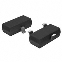
- 封装类型:塑料表面贴装封装,3引脚SOT23。