BGU7063
Analog controlled high linearity low noise variable gain
amplifier
Rev. 2 — 7 December 2012
Product data sheet
1. Product profile
1.1 General description
The BGU7063 is a fully integrated analog-controlled variable gain amplifier module. Its
low noise and high linearity performance makes it ideal for sensitive receivers in cellular
base station applications. The BGU7063 is operating in the 1920 MHz to 1980 MHz
frequency range and has a gain control range of 35 dB. At maximum gain the noise figure
is 0.9 dB. The gain is analog-controlled having maximum gain at 0 V and minimum gain at
3.3 V. The LNA can be bypassed extending the dynamic range. The BGU7063 is
internally matched to 50 ohm, meaning no external matching is required, enabling ease of
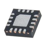
use. It is housed in a 16 pins 8 mm 8 mm 1.3 mm leadless HLQFN16R package
SOT1301.
1.2 Features and benefits
Input and output internally matched to 50
Low noise figure of 0.9 dB
High input IP3 of 0.9 dBm
High Pi(1dB) of 12.5 dBm
Bypass mode of LNA giving high dynamic gain range
Gain control range of 0 dB to 35 dB
Single 5 V supply
Single analog gain control of 0 V to 3.3 V
Unconditionally stable up to 12.75 GHz
Moisture sensitivity level 3
ESD protection at all pins
1.3 Applications
Cellular base stations, remote radio heads
3G, LTE infrastructure
Low noise applications with variable gain and high linearity requirements
Active antenna
�BGU7063
NXP Semiconductors
Analog controlled high linearity low noise variable gain amplifier
1.4 Quick reference data
Table 1.
Quick reference data
VCC1 = 5 V; VCC2 = 5 V; f = 1950 MHz; Tamb = 25 C; input and output 50 ; unless otherwise specified.
Symbol Parameter
ICC(tot)
NF
Conditions
total supply current
noise figure
input third-order intercept point
IP3I
Pi(1dB)
Min Typ
Max Unit
high gain mode
[1]
200 230
265
mA
low gain mode
[2]
165 190
215
mA
Vctrl(Gp) = 0 V (maximum power gain)
[1]
-
0.9
-
dB
Gp = 35 dB
[1]
-
1.05
1.2
dB
Gp = 35 dB; 2-tone; tone-spacing = 1.0 MHz
[1]
0
0.9
-
dBm
[1]
14 12.5 -
dBm
input power at 1 dB gain compression Gp = 35 dB
[1]
high gain mode: GS1 = LOW; GS2 = HIGH (see Table 9)
[2]
low gain mode: GS1 = HIGH; GS2 = LOW (see Table 9)
2. Pinning information
���
,,�
,,#
���
��
�&
�'
�������
��
���� �����
�!
2.1 Pinning
�"�
'
�+
��
�
��
�
&
(
��
����
%
���
��
�
��
$
#
��
�
���
!
���)*�
�"#
�#
�
�
��
�
�����
DDD�������
��������������������
Fig 1.
Pin configuration
2.2 Pin description
Table 2.
BGU7063
Product data sheet
Pin description
Symbol
Pin
Description
RF_IN
1
RF input
GND
2, 11, 13, 16
ground
GS1
3
gain switch control 1
n.c.
4, 5, 7, 10
not connected, internally open
All information provided in this document is subject to legal disclaimers.
Rev. 2 — 7 December 2012
© NXP B.V. 2012. All rights reserved.
2 of 16
�BGU7063
NXP Semiconductors
Analog controlled high linearity low noise variable gain amplifier
Table 2.
Pin description …continued
Symbol
Pin
Description
GS2
6
gain switch control 2
i.c.
8
internally connected to ground
Vctrl(Gp)
9
power gain control voltage
RF_OUT
12
RF output
VCC2
14
supply voltage 2
VCC1
15
supply voltage 1
3. Ordering information
Table 3.
Ordering information
Type number Package
Name
BGU7063
Description
Version
HLQFN16R plastic thermal enhanced low profile quad flat package; SOT1301-1
no leads; 16 terminals; body 8 8 1.3 mm
5)B,1
9&&�
9&&�
*1'
WHUPLQDO��
LQGH[�DUHD
*1'
4. Functional diagram
��
��
��
��
�
��
5)B287
��
*1'
%
很抱歉,暂时无法提供与“BGU7063,518”相匹配的价格&库存,您可以联系我们找货
免费人工找货