XS
ON
6
BGU8009
SiGe:C low-noise amplifier MMIC for GPS, GLONASS, Galileo
and COMPASS and LTE B32
Rev. 7.3 — 16 May 2019
1
Product data sheet
General description
The BGU8009 is, also known as the GPS1201M, a Low-Noise Amplifier (LNA) for GNSS
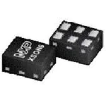
receiver and LTE Band 32 down link applications. This BGU8009 is available in a small
plastic 6-pin extremely thin leadless package. The BGU8009 requires one external
matching inductor and one external decoupling capacitor.
The BGU8009 adapts itself to the changing environment resulting from co-habitation
of different radio systems in modern cellular handsets. It has been designed for low
power consumption and optimal performance when jamming signals from co-existing
cellular transmitters are present. At low jamming power levels, it delivers 18 dB gain at a
noise figure of 0.65 dB. During high jamming power levels, resulting, for example from a
cellular transmit burst, it temporarily increases its bias current to improve sensitivity.
2
Features and benefits
• Covers full GNSS L1 band, from 1559 MHz to 1610 MHz and LTE band 32 from 1452
MHz to 1496 MHz
• Optionally also the GNSS lower L-band can be covered (from 1164 MHz to 1299
MHz) by adding additional matching components as described in the application note
AN11353.
• GNSS:
– Noise figure = 0.65 dB
– Gain 18 dB
– High input 1 dB compression point of -7 dBm
– High out of band IP3i of 6 dBm
• LTE B32:
– Noise figure = 0.65 dB
– Gain 20 dB
– High input 1 dB compression point of -8.5 dBm
• Supply voltage 1.5 V to 3.1 V
• Optimized performance at low supply current of 4.2 mA
• Power-down mode current consumption < 1 µA
• Integrated temperature stabilized bias for easy design.
• Requires only one input matching inductor and one supply decoupling capacitor
• Input and output DC decoupled
• ESD protection on all pins (HBM > 2 kV)
• Integrated matching for the output
• Available in a 6-pins leadless package 1.1 mm x 0.9 mm x 0.47 mm; 0.4 mm pitch:
SOT1230
• 180 GHz transit frequency - SiGe:C technology
• Moisture sensitivity level 1
�BGU8009
NXP Semiconductors
SiGe:C low-noise amplifier MMIC for GPS, GLONASS, Galileo and COMPASS and LTE B32
3
Applications
•
•
•
•
•
•
•
•
BGU8009
Product data sheet
Smart phones
Feature phones
Tablets
Digital still cameras
Digital video cameras
RF front-end modules
Complete GNSS modules
Personal health applications
All information provided in this document is subject to legal disclaimers.
Rev. 7.3 — 16 May 2019
© NXP B.V. 2019. All rights reserved.
2 / 25
�BGU8009
NXP Semiconductors
SiGe:C low-noise amplifier MMIC for GPS, GLONASS, Galileo and COMPASS and LTE B32
4
Quick reference data
Table 1. Quick reference data GNSS band L1
f = 1575 MHz; VCC = 2.85 V; Pi < -40 dBm; Tamb = 25 °C; input matched to 50 Ω using a 5.6 nH inductor, see Figure 34,
unless otherwise specified.
Symbol
Parameter
VCC
supply voltage
ICC
supply current
Gp
Conditions
Min
Typ
Max
Unit
1.5
-
3.1
V
• Pi < -40 dBm
2.6
4.4
6.5
mA
• Pi = -20 dBm
-
9
-
mA
Pi < -40 dBm
16
17.8
20
dB
VI(ENABLE) ≥ 0.8 V
power gain
Pi = -20 dBm
NF
noise figure
Pi(1dB)
IP3i
[1]
[2]
-
20.0
-
dB
Pi < -40 dBm
[1]
-
0.65
1.2
dB
Pi < -40 dBm
[1]
-
0.70
1.25
dB
-
-10
-
dBm
VCC = 1.8 V
input power at 1 dB gain
compression
VCC = 2.85 V
input third-order intercept point
-12.5
-7
-
dBm
VCC = 1.8 V
[2]
-
3
-
dBm
VCC = 2.85 V
[2]
-
6
-
dBm
PCB losses are subtracted.
f 1 = 1713 MHz; f2 = 1851 MHz; Pi = -20 dBm per carrier
Table 2. Quick reference data LTE B32
f = 1474 MHz; VCC = 2.8 V; Pi = -30 dBm; Tamb = 25 °C; input matched to 50 Ω using a 9.1 nH inductor, see Figure 34,
unless otherwise specified.
Symbol
Parameter
VCC
supply voltage
ICC
supply current
Gp
power gain
Conditions
VI(ENABLE) ≥ 0.8 V
noise figure
Pi(1dB)
input power at 1 dB gain compression
VCC = 1.8 V
VCC = 2.8 V
[1]
[2]
Typ
Max
Unit
1.5
-
3.1
V
-
4.4
-
mA
20
[1]
NF
IP3i
Min
input third-order intercept point
dB
-
0.65
-
dB
-
-11
-
dBm
-
-8.5
-
dBm
VCC = 1.8 V
[2]
-
-7
-
dBm
VCC = 2.8 V
[2]
-
-6
-
dBm
PCB losses are subtracted.
Δf = 1 MHz; Pi = -30 dBm per carrier.
BGU8009
Product data sheet
All information provided in this document is subject to legal disclaimers.
Rev. 7.3 — 16 May 2019
© NXP B.V. 2019. All rights reserved.
3 / 25
�BGU8009
NXP Semiconductors
SiGe:C low-noise amplifier MMIC for GPS, GLONASS, Galileo and COMPASS and LTE B32
5
Ordering information
Table 3. Ordering information
Type number
Package
Name
Description
Version
BGU8009
XSON6
plastic very thin small outline package; no leads; 6 terminals;
body 1.1 x 0.9 x 0.47 mm
SOT1230
OM7820
EVB
BGU8009 evaluation board, MMIC only
-
OM7824
EVB
BGU8009 evaluation board, front-end EVB
-
OM17066
EVB
BGU8009 evaluation board for LTE B32
6
Marking
Table 4. Marking code
Type number
Marking code
Date code
BGU8009
A
YWW
one digit device name
YWW
pin one identifier
plant code identifier
aaa-034078
Figure 1. Marking diagram
7
Block diagram
VCC
BGU8009
ENABLE
RF_IN
6
2
BIAS/CONTROL
5
3
RF_OUT
1, 4
aaa-022360
Figure 2. Block diagram
BGU8009
Product data sheet
All information provided in this document is subject to legal disclaimers.
Rev. 7.3 — 16 May 2019
© NXP B.V. 2019. All rights reserved.
4 / 25
�BGU8009
NXP Semiconductors
SiGe:C low-noise amplifier MMIC for GPS, GLONASS, Galileo and COMPASS and LTE B32
8
Pinning information
8.1 Pinning
BGU8009
GND_RF
4
3
RF_OUT
RF_IN
5
2
VCC
ENABLE
6
1
GND
Transparent top view
aaa-022136
Figure 3. Pin configuration
8.2 Pin description
Table 5. Pin description
9
Symbol
Pin
Description
GND
1
ground
VCC
2
supply voltage
RF_OUT
3
RF output
GND_RF
4
RF ground
RF_IN
5
RF input
ENABLE
6
enable
Limiting values
Table 6. Limiting values
In accordance with the Absolute Maximum Rating System (IEC 60134). Absolute Maximum Ratings are given as Limiting
Values of stress conditions during operation, that must not be exceeded under the worst probable conditions.
Symbol
VCC
Parameter
Conditions
supply voltage
Min
Max
Unit
[1]
-0.5
+5.0
V
[1] [2]
-0.5
+5.0
V
VI(ENABLE)
input voltage on pin
ENABLE
VI(ENABLE) < VCC + 0.6 V
VI(RF_IN)
input voltage on pin
RF_IN
DC, VI(RF_IN) < VCC + 0.6 V
[1] [2] [3]
-0.5
+5.0
V
VI(RF_OUT)
input voltage on pin
RF_OUT
DC, VI(RF_OUT) < VCC + 0.6 V
[1] [2] [3]
-0.5
+5.0
V
Pi
input power
1575 MHz
[1]
-
10
dBm
1474 MHz
[1]
-
10
dBm
-
55
mW
Ptot
total power dissipation
BGU8009
Product data sheet
Tsp ≤ 130 °C
All information provided in this document is subject to legal disclaimers.
Rev. 7.3 — 16 May 2019
© NXP B.V. 2019. All rights reserved.
5 / 25
�BGU8009
NXP Semiconductors
SiGe:C low-noise amplifier MMIC for GPS, GLONASS, Galileo and COMPASS and LTE B32
Symbol
Parameter
Tstg
Min
Max
Unit
storage temperature
-65
+150
°C
Tj
junction temperature
-
150
°C
VESD
electrostatic discharge
voltage
Human Body Model (HBM)
according to JEDEC standard
JS-001-2010
-
±2
kV
Charged Device Model (CDM)
according to JEDEC standard
JESD22-C101C
-
±1
kV
[1]
[2]
[3]
Conditions
Stressed with pulses of 200 ms in duration, with application circuit as in Figure 34.
Warning: due to internal ESD diode protection, the applied DC voltage shall not exceed VCC + 0.6 V and shall not exceed 5.0 V to avoid excess current.
The RF input and RF output are AC coupled through internal DC blocking capacitors.
10 Recommended operating conditions
Table 7. Operating conditions
Symbol
Parameter
VCC
Conditions
Min
Typ
Max
Unit
supply voltage
1.5
-
3.1
V
Tamb
ambient temperature
-40
+25
+85
°C
VI(ENABLE)
input voltage on pin ENABLE
OFF state
-
-
0.3
V
ON state
0.8
-
-
V
11 Thermal characteristics
Table 8. Thermal characteristics
Symbol
Parameter
Rth(j-sp)
thermal resistance from junction to solder point
BGU8009
Product data sheet
Conditions
All information provided in this document is subject to legal disclaimers.
Rev. 7.3 — 16 May 2019
Typ
Unit
225
K/W
© NXP B.V. 2019. All rights reserved.
6 / 25
�BGU8009
NXP Semiconductors
SiGe:C low-noise amplifier MMIC for GPS, GLONASS, Galileo and COMPASS and LTE B32
12 Characteristics GNSS band L1
Table 9. Characteristics at VCC = 1.8 V
f = 1575 MHz; VCC = 1.8 V; VI(ENABLE) >= 0.8 V; Pi < -40 dBm; Tamb = 25 °C; input matched to 50 Ω using a 5.6 nH inductor,
see Figure 34, unless otherwise specified.
Symbol
Parameter
Conditions
ICC
supply current
VI(ENABLE) ≥ 0.8 V
Gp
RLout
ISL
input return loss
output return loss
noise figure
Pi(1dB)
input power at 1 dB gain
compression
IP3i
input third-order intercept point
Max Unit
-
Pi < -40 dBm
2.3
4.2
6.2 mA
Pi = -20 dBm
-
9
- mA
VI(ENABLE) ≤ 0.3 V
-
-
1 μA
16 17.6
20 dB
Pjam = -20 dBm; fjam = 850 MHz
- 19.8
- dB
Pjam = -20 dBm; fjam = 1850 MHz
- 20.0
- dB
Pi < -40 dBm
-
9
- dB
Pi = -20 dBm
-
11
- dB
Pi < -40 dBm
-
15
- dB
Pi = -20 dBm
-
15
- dB
-
37
- dB
0.65
1.2 dB
isolation
NF
Typ
-
no jammer
power gain
RLin
Min
Pi = -40 dBm; no jammer
[1]
Pi = -40 dBm; no jammer
[2] [1]
-
- -
- 0.70 1.25 dB
Pjam = -20 dBm; fjam = 850 MHz
[2]
-
0.9
- dB
Pjam = -20 dBm; fjam = 1850 MHz
[2]
-
1.2
- dB
[1]
- -10
- dBm
[1] [3]
-
3
-
dBm
[1] [4]
-
3
-
dBm
ton
turn-on time
time from VI(ENABLE) ON to 90 % of the
gain
-
-
2
µs
toff
turn-off time
time from VI(ENABLE) OFF to 10 % of
the gain
-
-
1
µs
[1]
[2]
[3]
[4]
Guaranteed by device design; not tested in production.
Including PCB losses.
f1 = 1713 MHz; f2 = 1851 MHz, Pi = -20 dBm per carrier.
f1 = 1713 MHz; f2 = 1851 MHz, Pi(1) = -20 dBm, Pi(2) = -65 dBm.
BGU8009
Product data sheet
All information provided in this document is subject to legal disclaimers.
Rev. 7.3 — 16 May 2019
© NXP B.V. 2019. All rights reserved.
7 / 25
�BGU8009
NXP Semiconductors
SiGe:C low-noise amplifier MMIC for GPS, GLONASS, Galileo and COMPASS and LTE B32
Table 10. Characteristics at Vcc = 2.85 V
f = 1575 MHz; VCC = 2.85 V; VI(ENABLE) >= 0.8 V; Pi < -40 dBm; Tamb = 25 °C; input matched to 50 Ω using a 5.6 nH
inductor,see Figure 34, unless otherwise specified.
Symbol
Parameter
Conditions
Min
Typ
Max Unit
ICC
supply current
VI(ENABLE) ≥ 0.8 V
-
-
-
-
• Pi < -40 dBm
2.6
4.4
6.5
mA
• Pi = -20 dBm
-
9
-
mA
VI(ENABLE) ≤ 0.3 V
-
-
1
µA
no jammer
16
17.8 20
dB
• Pjam = -20 dBm; fjam = 850 MHz
-
20.0 -
dB
• Pjam = -20 dBm; fjam = 1850 MHz
-
20.2 -
dB
Pi < -40 dBm
-
9
-
dB
Pi = -20 dBm
-
11
-
dB
Pi < -40 dBm
-
15
-
dB
Pi = -20 dBm
-
15
-
dB
-
dB
Gp
power gain
RLin
RLout
ISL
input return loss
output return loss
isolation
NF
noise figure
Pi(1dB)
-
37
Pi = -40 dBm; no jammer
[1]
-
0.65 1.2
Pi = -40 dBm; no jammer
[2] [1]
-
0.70 1.25 dB
Pjam = -20 dBm; fjam = 850 MHz
[2]
-
0.9
-
dB
Pjam = -20 dBm; fjam = 1850 MHz
[2]
-
1.2
-
dB
[1]
-12
.5
-7
-
dBm
[1] [3]
0
6
-
dBm
[1] [4]
0
6
-
dBm
input power at 1 dB
gain compression
IP3i
input third-order intercept point
dB
ton
turn-on time
time from VI(ENABLE) ON to 90 % of the
gain
-
-
2
µs
toff
turn-off time
time from VI(ENABLE) OFF to 10 % of
the gain
-
-
1
µs
[1]
[2]
[3]
[4]
Guaranteed by device design; not tested in production.
Including PCB losses.
f1 = 1713 MHz; f2 = 1851 MHz, Pi = -20 dBm per carrier.
f1 = 1713 MHz; f2 = 1851 MHz, Pi(1) = -20 dBm, Pi(2) = -65 dBm.
BGU8009
Product data sheet
All information provided in this document is subject to legal disclaimers.
Rev. 7.3 — 16 May 2019
© NXP B.V. 2019. All rights reserved.
8 / 25
�BGU8009
NXP Semiconductors
SiGe:C low-noise amplifier MMIC for GPS, GLONASS, Galileo and COMPASS and LTE B32
13 Graphs GNSS band L1
ICC
(mA)
aaa-006462
5
ICC
(mA)
4.5
aaa-006463
5
4.5
(3)
(2)
(1)
4
3.5
3
(4)
(3)
(2)
(1)
4
3.5
1
1.5
2
2.5
3
VCC (V)
3
-55
3.5
-35
-15
5
25
45
65
85
Tamb (°C)
105
Pi = -45 dBm.
(1) Tamb = -40 °C
(2) Tamb = +25 °C
(3) Tamb = +85 °C
Pi = -45 dBm.
(1) VCC = 1.5 V
(2) VCC = 1.8 V
(3) VCC = 2.85 V
(4) VCC = 3.1 V
Figure 4. Supply current as a function of supply
voltage; typical values
Figure 5. Supply current as a function of ambient
temperature; typical values
Gp
(dB)
aaa-006464
20
Gp
(dB)
aaa-006465
24
20
16
16
12
(1)
(2)
(3)
(4)
(3)
(2)
(1)
12
8
8
4
0
500
4
1000
1500
Pi = -45 dBm; VCC = 1.8 V.
(1) Tamb = -40 °C
(2) Tamb = +25 °C
(3) Tamb = +85 °C
2000
2500
f (MHz)
3000
0
500
1000
1500
2000
2500
f (MHz)
3000
Tamb = 25 °C; VCC = 1.8 V.
(1) Pi = -45 dBm
(2) Pi = -30 dBm
(3) Pi =- 20 dBm
(4) Pi = -15 dBm
Figure 6. Power gain as a function of frequency; typical Figure 7. Power gain as a function of frequency; typical
values
values
BGU8009
Product data sheet
All information provided in this document is subject to legal disclaimers.
Rev. 7.3 — 16 May 2019
© NXP B.V. 2019. All rights reserved.
9 / 25
�BGU8009
NXP Semiconductors
SiGe:C low-noise amplifier MMIC for GPS, GLONASS, Galileo and COMPASS and LTE B32
Gp
(dB)
aaa-006466
20
Gp
(dB)
18
ICC
(mA)
Gp
16
18
12
(4)
(3)
(2)
(1)
8
10
1000
1500
2000
2500
f (MHz)
3000
Pi = -45 dBm; Tamb = 25 °C.
(1) VCC = 1.5 V
(2) VCC = 1.8 V
(3) VCC = 2.85 V
(4) VCC = 3.1 V
6
-50
14
(4)
(3)
(2)
(1)
14
4
0
500
aaa-006467
22
ICC
10
(1)
(2)
(3)
(4)
6
-40
-30
-20
Pi (dBm)
2
-10
f = 1575 MHz; Tamb= 25 °C.
(1) VCC = 1.5 V
(2) VCC = 1.8 V
(3) VCC = 2.85 V
(4) VCC = 3.1 V
Figure 8. Power gain as a function of frequency; typical Figure 9. Power gain and supply current as function of
values
input power; typical values
NF
(dB)
aaa-006468
1
0.8
1.2
(3)
(1)
(2)
(3)
(4)
0.6
0.8
0.4
0.2
1500
aaa-006469
1.6
NF
(dB)
(2)
(1)
0.4
1525
1550
1575
1600
1625
f (MHz)
1650
0
1.4
1.8
2.2
2.6
3
VCC (V)
3.4
Tamb = 25 °C; no jammer, including PCB losses.
(1) VCC = 1.5 V
(2) VCC = 1.8 V
(3) VCC = 2.85 V
(4) VCC = 3.1 V
f = 1575 MHz; no jammer, including PCB losses.
(1) Tamb = -40 °C
(2) Tamb = +25 °C
(3) Tamb = +85 °C
Figure 10. Noise figure as a function of frequency;
typical values
Figure 11. Noise figure as a function of supply voltage;
typical values
BGU8009
Product data sheet
All information provided in this document is subject to legal disclaimers.
Rev. 7.3 — 16 May 2019
© NXP B.V. 2019. All rights reserved.
10 / 25
�BGU8009
NXP Semiconductors
SiGe:C low-noise amplifier MMIC for GPS, GLONASS, Galileo and COMPASS and LTE B32
1.4
NF
(dB)
1.2
aaa-006471
3
NF
(dB)
2.5
aaa-006470
(1)
(2)
(4)
(3)
2
1
1.5
0.8
1
(1)
(2)
(3)
(4)
0.6
0.5
0.4
0.2
-50
0
-50
-25
0
25
50
75
Tamb (°C)
-40
-30
-20
100
-10
Pjam (dBm)
0
f = 1575 MHz; no jammer, including PCB losses.
(1) VCC = 1.5 V
(2) VCC = 1.8 V
(3) VCC = 2.85 V
(4) VCC = 3.1 V
fjam = 850 MHz; Tamb= 25 °C; f = 1575 MHz; including PCB
losses.
(1) VCC = 1.5 V
(2) VCC = 1.8 V
(3) VCC = 2.85 V
(4) VCC = 3.1 V
Figure 12. Noise figure as a function of ambient
temperature; typical values
Figure 13. Noise figure as a function of jamming power;
typical values
aaa-006472
3
NF
(dB)
2.5
RLin
(dB)
aaa-006473
0
-3
2
(1)
(2)
(3)
(4)
1.5
(3)
(2)
(1)
-6
1
-9
0.5
0
-50
-40
-30
-20
-10
Pjam (dBm)
0
fjam = 1850 MHz; Tamb= 25 °C; f = 1575 MHz; including PCB
losses.
(1) VCC = 1.5 V
(2) VCC = 1.8 V
(3) VCC = 2.85 V
(4) VCC = 3.1 V
-12
500
1000
1500
2000
2500
f (MHz)
3000
Pi = -45 dBm; VCC= 1.8 V.
(1) Tamb = -40 °C
(2) Tamb = +25 °C
(3) Tamb = +85 °C
Figure 14. Noise figure as a function of jamming power; Figure 15. Input return loss as a function of frequency;
typical values
typical values
BGU8009
Product data sheet
All information provided in this document is subject to legal disclaimers.
Rev. 7.3 — 16 May 2019
© NXP B.V. 2019. All rights reserved.
11 / 25
�BGU8009
NXP Semiconductors
SiGe:C low-noise amplifier MMIC for GPS, GLONASS, Galileo and COMPASS and LTE B32
RLin
(dB)
aaa-006474
0
RLin
(dB)
-2
-2
-4
-4
(1)
(2)
(3)
(4)
-6
-8
-10
-10
1000
1500
(1)
(2)
(4)
(3)
-6
-8
-12
500
aaa-006475
0
2000
2500
f (MHz)
3000
-12
500
1000
1500
2000
2500
f (MHz)
3000
Tamb = 25 °C; VCC= 1.8 V.
(1) Pi = -45 dBm
(2) Pi = -30 dBm
(3) Pi = -20 dBm
(4) Pi = -15 dBm
Pi = -45 dBm; Tamb= 25 °C.
(1) VCC = 1.5 V
(2) VCC = 1.8 V
(3) VCC = 2.85 V
(4) VCC = 3.1 V
Figure 16. Input return loss as a function of frequency;
typical values
Figure 17. Input return loss as a function of frequency;
typical values
RLin
(dB)
aaa-006476
0
RLout
(dB)
aaa-006477
0
-4
-4
(4)
(3)
(2)
(1)
-8
-8
-12
-12
(3)
(2)
(1)
-16
-16
-20
-50
-20
-40
-30
-20
Pi (dBm)
-10
-24
500
1000
1500
2000
2500
f (MHz)
3000
f = 1575 MHz; Tamb = 25 °C.
(1) VCC = 1.5 V
(2) VCC = 1.8 V
(3) VCC = 2.85 V
(4) VCC = 3.1 V
Pi = -45 dBm; VCC = 1.8 V.
(1) Tamb = -40 °C
(2) Tamb = +25 °C
(3) Tamb = +85 °C
Figure 18. Input return loss as a function of input
power; typical values
Figure 19. Output return loss as a function of
frequency; typical values
BGU8009
Product data sheet
All information provided in this document is subject to legal disclaimers.
Rev. 7.3 — 16 May 2019
© NXP B.V. 2019. All rights reserved.
12 / 25
�BGU8009
NXP Semiconductors
SiGe:C low-noise amplifier MMIC for GPS, GLONASS, Galileo and COMPASS and LTE B32
RLout
(dB)
aaa-006478
0
RLout
(dB)
-4
-4
-8
-8
-12
-12
-16
-20
500
1500
(4)
(3)
(2)
(1)
-16
(4)
(3)
(2)
(1)
1000
aaa-006479
0
2000
2500
f (MHz)
3000
-20
500
1000
1500
2000
2500
f (MHz)
3000
Tamb = 25 °C; VCC = 1.8 V.
(1) Pi = -45 dBm
(2) Pi = -30 dBm
(3) Pi = -20 dBm
(4) Pi = -15 dBm
Pi= -45 dBm; Tamb = 25 °C.
(1) VCC = 1.5 V
(2) VCC = 1.8 V
(3) VCC = 2.85 V
(4) VCC = 3.1 V
Figure 20. Output return loss as a function of
frequency; typical values
Figure 21. Output return loss as a function of
frequency; typical values
RLout
(dB)
aaa-006480
0
-4
-8
ISL
(dB)
-10
(1)
(2)
(3)
(4)
-20
-12
-30
-16
-40
-20
-50
-40
aaa-006481
0
-30
-20
Pi (dBm)
-10
-50
500
(1)
(2)
(3)
1000
1500
2000
2500
f (MHz)
3000
f = 1575 MHz; Tamb = 25 °C.
(1) VCC = 1.5 V
(2) VCC = 1.8 V
(3) VCC = 2.85 V
(4) VCC = 3.1 V
Pi = -45 dBm; VCC = 1.8 V.
(1) Tamb = -40 °C
(2) Tamb = +25 °C
(3) Tamb = +85 °C
Figure 22. Output return loss as a function of input
power; typical values
Figure 23. Isolation as a function of frequency; typical
values
BGU8009
Product data sheet
All information provided in this document is subject to legal disclaimers.
Rev. 7.3 — 16 May 2019
© NXP B.V. 2019. All rights reserved.
13 / 25
�BGU8009
NXP Semiconductors
SiGe:C low-noise amplifier MMIC for GPS, GLONASS, Galileo and COMPASS and LTE B32
ISL
(dB)
aaa-006482
0
-10
-10
-20
-20
(4)
(3)
(2)
(1)
-30
-30
-40
-50
500
aaa-006483
0
ISL
(dB)
(3)
(2)
(1)
(4)
-40
1000
1500
2000
2500
f (MHz)
3000
-50
500
1000
1500
2000
2500
f (MHz)
3000
Tamb = 25 °C; VCC = 1.8 V.
(1) Pi = -45 dBm
(2) Pi = -30 dBm
(3) Pi = -20 dBm
(4) Pi = -15 dBm
Pi = -45 dBm; Tamb = 25 °C.
(1) VCC = 1.5 V
(2) VCC = 1.8 V
(3) VCC = 2.85 V
(4) VCC = 3.1 V
Figure 24. Isolation as a function of frequency; typical
values
Figure 25. Isolation as a function of frequency; typical
values
ISL
(dB)
aaa-006484
0
Pi(1dB)
(dBm)
aaa-006485
0
-4
-10
-8
-20
-30
-40
-50
-12
(2)
(1)
(3)
(4)
-40
f = 1575 MHz; Tamb = 25 °C.
(1) VCC = 1.5 V
(2) VCC = 1.8 V
(3)VCC = 2.85 V
(4)VCC = 3.1 V
-30
(3)
(2)
(1)
-16
-20
Pi (dBm)
-10
-20
1
1.5
2
2.5
3
VCC (V)
3.5
f = 850 MHz.
(1) Tamb = -40 °C
(2) Tamb = +25 °C
(3) Tamb = +85 °C
Figure 26. Isolation as a function of input power; typical Figure 27. Input power at 1 dB gain compression as a
values
function of supply voltage; typical values
BGU8009
Product data sheet
All information provided in this document is subject to legal disclaimers.
Rev. 7.3 — 16 May 2019
© NXP B.V. 2019. All rights reserved.
14 / 25
�BGU8009
NXP Semiconductors
SiGe:C low-noise amplifier MMIC for GPS, GLONASS, Galileo and COMPASS and LTE B32
Pi(1dB)
(dBm)
aaa-006486
0
Pi(1dB)
(dBm)
-4
-4
-8
-8
(3)
(2)
(1)
-12
-12
-16
-16
-20
aaa-006487
0
1
1.5
2
2.5
3
VCC (V)
3.5
-20
(3)
(2)
(1)
1
1.5
2
2.5
3
VCC (V)
3.5
f = 1850 MHz.
(1) Tamb = -40 °C
(2) Tamb = +25 °C
(3) Tamb= +85 °C
f = 1575 MHz.
(1) Tamb = -40 °C
(2) Tamb = +25 °C
(3) Tamb = +85 °C
Figure 28. Input power at 1 dB gain compression as a
function of supply voltage; typical values
Figure 29. Input power at 1 dB gain compression as a
function of supply voltage; typical values
aaa-006488
10
PL
(dBm)
-10
IMD3
(dBm)
-10
PL
(1)
(2)
(3)
(4)
-30
10
-50
-70
aaa-006489
10
PL
(dBm)
-10
-30
-30
-50
-50
-70
-70
-30
(1)
(1)
(2)
(2)
(3)
(3)
-50
-70
IMD3
-90
-90
-40
IMD3
(dBm)
-10
PL
IMD3
-110
-50
10
-30
-20
Pi (dBm)
-110
-10
Tamb = 25 °C; f = 1575 MHz; f1 = 1713 MHz; f2 = 1851 MHz;
Pi per carrier.
(1) VCC = 1.5 V
(2) VCC = 1.8 V
(3) VCC = 2.85 V
(4) VCC = 3.1 V
-90
-110
-50
-90
-40
-30
-20
Pi (dBm)
-110
-10
VCC = 2.85 V; f = 1575 MHz; f1 = 1713 MHz; f2 = 1851 MHz;
Pi per carrier.
(1) Tamb = - 40 °C
(2) Tamb = +25 °C
(3) Tamb = +85 °C
Figure 30. Output power and third order intermodulation Figure 31. Output power and third order intermodulation
distortion as function of input power; typical values
distortion as function of input power; typical values
BGU8009
Product data sheet
All information provided in this document is subject to legal disclaimers.
Rev. 7.3 — 16 May 2019
© NXP B.V. 2019. All rights reserved.
15 / 25
�BGU8009
NXP Semiconductors
SiGe:C low-noise amplifier MMIC for GPS, GLONASS, Galileo and COMPASS and LTE B32
K
aaa-006490
102
K
aaa-006491
102
(4)
(3)
(1)
(2)
(3)
(2)
(1)
10
1
0
2000
4000
10
6000
8000
f (MHz)
10000
1
0
2000
4000
6000
8000
f (MHz)
10000
VCC = 1.8 V; Pi = -45 dBm.
(1) Tamb = -40 °C
(2) Tamb = +25 °C
(3) Tamb = +85 °C
Tamb = 25 °C; Pi = -45 dBm.
(1) VCC = 1.5 V
(2) VCC = 1.8 V
(3) VCC = 2.85 V
(4) VCC = 3.1 V
Figure 32. Rollett stability factor as a function of
frequency; typical values
Figure 33. Rollett stability factor as a function of
frequency; typical values
BGU8009
Product data sheet
All information provided in this document is subject to legal disclaimers.
Rev. 7.3 — 16 May 2019
© NXP B.V. 2019. All rights reserved.
16 / 25
�BGU8009
NXP Semiconductors
SiGe:C low-noise amplifier MMIC for GPS, GLONASS, Galileo and COMPASS and LTE B32
14 Characteristics LTE B32
Table 11. Characteristics
1474 MHz; VCC = 1.8 V; Pi = -30 dBm; Tamb = 25 °C; input matched 50 Ω using application diagram from Figure 34 and
component values as in Table 14. Unless otherwise specified.
Symbol Parameter
Conditions
Min
Typ
Max Unit
VI(ENABLE) ≥ 0.8 V
-
4.4
-
mA
Gain Mode
ICC
supply current
Gp
power gain
-
20
-
dB
RLin
input return loss
-
17.5 -
dB
RLout
output return loss
-
23.5 -
dB
ISL
isolation
-
36
dB
NF
[1] [2]
noise figure
-
-
0.65 -
dBm
[2]
-
-11
-
dBm
[2] [3]
-
-7
-
dBm
Pi(1dB)
input power at 1 dB gain
compression
IP3i
input third-order intercept point Δf = 1 MHz, Pi = -30 dBm
ton
turn-on time
Time from VI(CTRL) ON to 90 % of the gain
-
-
2
µs
toff
turn-off time
Time from VI(CTRL) OFF to 10 % of the gain
-
-
1
µs
K
Rollett stability factor
1
-
-
-
[1]
[2]
[3]
PCB losses are subtracted.
Guaranteed by device design; not tested in production.
f1= 1474 MHz, f2 = 1475 MHz
Table 12. Characteristics
1474 MHz; VCC =2.8 V; Pi = -30 dBm; Tamb = 25 °C; input matched 50 Ω using application diagram from Figure 34 and
component values as in Table 14. Unless otherwise specified.
Symbol Parameter
Conditions
Min
Typ
VI(ENABLE) ≥ 0.8 V
-
4.6
Max Unit
Gain Mode
ICC
supply current
Gp
power gain
-
20
-
dB
RLin
input return loss
-
17.5 -
dB
RLout
output return loss
-
23.5 -
dB
ISL
isolation
NF
noise figure
mA
-
36
-
dB
[1] [2]
-
0.65 -
dB
[2]
-
-8.5
dBm
[2] [3]
-
-6
Pi(1dB)
input power at 1 dB gain
compression
IP3i
input third-order intercept point Δf = 1 MHz, Pi = - 30 dBm
ton
turn-on time
Time from VI(CTRL) ON to 90 % of the gain
-
-
2
µs
toff
turn-off time
Time from VI(CTRL) OFF to 10 % of the gain
-
-
1
µs
K
Rollett stability factor
1
-
-
-
BGU8009
Product data sheet
All information provided in this document is subject to legal disclaimers.
Rev. 7.3 — 16 May 2019
-
dBm
© NXP B.V. 2019. All rights reserved.
17 / 25
�BGU8009
NXP Semiconductors
SiGe:C low-noise amplifier MMIC for GPS, GLONASS, Galileo and COMPASS and LTE B32
[1]
[2]
[3]
PCB losses are subtracted.
Guaranteed by device design; not tested in production.
f1= 1474 MHz, f2 = 1475 MHz
15 Application information
15.1 GNSS and LTE B32 LNA
Ven Vcc
RFin
L1
6
5
IC1
1
C1
RFout
2 3
4
aaa-006409
For a list of components, see Table 13 (GNSS) and Table 14 (LTE B32).
Figure 34. Schematics GNSS LNA and LTE B32 evaluation board
Table 13. List of components for GNSS applications
See Figure 34 for schematics.
Component
Description
Value
Remarks
EVB
Evaluation Board
SOT1230 - EVB
EVB for GNSS application, NXP
Semiconductors
C1
decoupling capacitor
1 nF
IC1
BGU8009
-
NXP Semiconductors
L1
high-quality matching inductor
5.6 nH
GNSS band L1: 1559 < f < 1610 MHz
Murata LQW15A
BGU8009
Product data sheet
All information provided in this document is subject to legal disclaimers.
Rev. 7.3 — 16 May 2019
© NXP B.V. 2019. All rights reserved.
18 / 25
�BGU8009
NXP Semiconductors
SiGe:C low-noise amplifier MMIC for GPS, GLONASS, Galileo and COMPASS and LTE B32
Table 14. List of components for LTE B32 applications
See Figure 34 for schematics.
Component
Description
Value
Remarks
EVB
Evaluation Board
OM17025
EVB for LTE application, NXP
Semiconductors
(SOT1230, SOT1232)
C1
decoupling capacitor
1 nF
IC1
BGU8009
-
NXP Semiconductors
L1
high-quality matching inductor
9.1 nH
LTE band 32 L1: 1452 < f < 1496 MHz
Murata LQW15A
GNSS: See application note AN11288 for details. LTE B32: See application note
AN11986.
BGU8009
Product data sheet
All information provided in this document is subject to legal disclaimers.
Rev. 7.3 — 16 May 2019
© NXP B.V. 2019. All rights reserved.
19 / 25
�BGU8009
NXP Semiconductors
SiGe:C low-noise amplifier MMIC for GPS, GLONASS, Galileo and COMPASS and LTE B32
16 Package outline
XSON6: plastic very thin small outline package; no leads; 6 terminals; body 1.1 x 0.9 x 0.47 mm
shape
optional (6×)
A
D
SOT1230
e
3
4
e1
E
v
e1
6
1
pin 1
index area
pin 1
index area
A1
B
y
v
y1 C
A
A B
A B
b (6×)
L
(6×)
C
shape
optional (4×)
0
1 mm
scale
Dimensions (mm are the original dimensions)
Unit
mm
A
A1
D
E
min 0.44
0.85 1.05
nom 0.47
0.90 1.10
max 0.50 0.04 0.95 1.15
e1
0.4
e
b
L
0.17 0.22
0.45 0.20 0.25
0.25 0.30
V
Y
Y1
0.1
0.05
0.1
Note
1. Dimension A is including plating thickness.
Outline
version
sot1230_po
References
IEC
JEDEC
JEITA
European
projection
Issue date
13-01-02
13-01-08
SOT1230
Figure 35. Package outline SOT1230 (XSON6)
BGU8009
Product data sheet
All information provided in this document is subject to legal disclaimers.
Rev. 7.3 — 16 May 2019
© NXP B.V. 2019. All rights reserved.
20 / 25
�BGU8009
NXP Semiconductors
SiGe:C low-noise amplifier MMIC for GPS, GLONASS, Galileo and COMPASS and LTE B32
17 Handling information
CAUTION
This device is sensitive to ElectroStatic Discharge (ESD). Observe
precautions for handling electrostatic sensitive devices.
Such precautions are described in the ANSI/ESD S20.20, IEC/ST 61340-5,
JESD625-A or equivalent standards.
18 Abbreviations
Table 15. Abbreviations
Acronym
Description
GLONASS
global navigation satellite system
GNSS
global navigation satellite system
GPS
global positioning system
HBM
human body model
MMIC
monolithic microwave-integrated circuit
PCB
printed-circuit board
SiGe:C
silicon germanium carbon
19 Revision history
Table 16. Revision history
Document ID
Release date
Data sheet status
Change notice
Supersedes
BGU8009 v.7.3
20190516
Product data sheet
-
BGU8009 v.7.2
Modifications:
• added general Marking diagram
BGU8009 v.7.2
20190510
-
BGU8009 v.7.1
Modifications:
• removed incorrect marking code description
• adapted date code notation to the Marking code table
BGU8009 v.7.1
20180416
-
BGU8009 v.7
Modifications:
• adapted the data sheet to the new look and feel
BGU8009 v.7
20170720
-
BGU8009 v.6
Modifications:
• Section 1 "General description" on page 1: added GPS1201M according to our new naming
convention
• Section 2 "Features and benefits" on page 1: added LTE B32 characteristics
• Section 14 "Characteristics LTE B32" on page 17 added
• Table 13 added EVB
BGU8009 v.6
20170118
Modifications:
• Section 1: added GPS1201M according to our new naming convention
BGU8009 v.5
20160405
Modifications:
• updated Figure 2
BGU8009 v.4
20160316
BGU8009
Product data sheet
Product data sheet
Product data sheet
Product data sheet
Product data sheet
-
BGU8009 v.5
Product data sheet
-
BGU8009 v.4
Product data sheet
-
BGU8009 v.3
All information provided in this document is subject to legal disclaimers.
Rev. 7.3 — 16 May 2019
© NXP B.V. 2019. All rights reserved.
21 / 25
�BGU8009
NXP Semiconductors
SiGe:C low-noise amplifier MMIC for GPS, GLONASS, Galileo and COMPASS and LTE B32
Document ID
Release date
Modifications:
• updated Table 8 and Table 9 on page 6
BGU8009 v.3
20141001
Modifications:
• Section 6.1 on page 3: Section has been added.
BGU8009 v.2
20130619
BGU8009 v.1
20130201
BGU8009
Product data sheet
Data sheet status
Change notice
Supersedes
-
BGU8009 v.2
Product data sheet
-
BGU8009 v.1
Product data sheet
-
-
Product data sheet
All information provided in this document is subject to legal disclaimers.
Rev. 7.3 — 16 May 2019
© NXP B.V. 2019. All rights reserved.
22 / 25
�BGU8009
NXP Semiconductors
SiGe:C low-noise amplifier MMIC for GPS, GLONASS, Galileo and COMPASS and LTE B32
20 Legal information
20.1 Data sheet status
Document status
[1][2]
Product status
[3]
Definition
Objective [short] data sheet
Development
This document contains data from the objective specification for product
development.
Preliminary [short] data sheet
Qualification
This document contains data from the preliminary specification.
Product [short] data sheet
Production
This document contains the product specification.
[1]
[2]
[3]
Please consult the most recently issued document before initiating or completing a design.
The term 'short data sheet' is explained in section "Definitions".
The product status of device(s) described in this document may have changed since this document was published and may differ in case of multiple
devices. The latest product status information is available on the Internet at URL http://www.nxp.com.
notice. This document supersedes and replaces all information supplied prior
to the publication hereof.
20.2 Definitions
Draft — The document is a draft version only. The content is still under
internal review and subject to formal approval, which may result in
modifications or additions. NXP Semiconductors does not give any
representations or warranties as to the accuracy or completeness of
information included herein and shall have no liability for the consequences
of use of such information.
Short data sheet — A short data sheet is an extract from a full data sheet
with the same product type number(s) and title. A short data sheet is
intended for quick reference only and should not be relied upon to contain
detailed and full information. For detailed and full information see the
relevant full data sheet, which is available on request via the local NXP
Semiconductors sales office. In case of any inconsistency or conflict with the
short data sheet, the full data sheet shall prevail.
Product specification — The information and data provided in a Product
data sheet shall define the specification of the product as agreed between
NXP Semiconductors and its customer, unless NXP Semiconductors and
customer have explicitly agreed otherwise in writing. In no event however,
shall an agreement be valid in which the NXP Semiconductors product
is deemed to offer functions and qualities beyond those described in the
Product data sheet.
20.3 Disclaimers
Limited warranty and liability — Information in this document is believed
to be accurate and reliable. However, NXP Semiconductors does not
give any representations or warranties, expressed or implied, as to the
accuracy or completeness of such information and shall have no liability
for the consequences of use of such information. NXP Semiconductors
takes no responsibility for the content in this document if provided by an
information source outside of NXP Semiconductors. In no event shall NXP
Semiconductors be liable for any indirect, incidental, punitive, special or
consequential damages (including - without limitation - lost profits, lost
savings, business interruption, costs related to the removal or replacement
of any products or rework charges) whether or not such damages are based
on tort (including negligence), warranty, breach of contract or any other
legal theory. Notwithstanding any damages that customer might incur for
any reason whatsoever, NXP Semiconductors’ aggregate and cumulative
liability towards customer for the products described herein shall be limited
in accordance with the Terms and conditions of commercial sale of NXP
Semiconductors.
Right to make changes — NXP Semiconductors reserves the right to
make changes to information published in this document, including without
limitation specifications and product descriptions, at any time and without
BGU8009
Product data sheet
Suitability for use — NXP Semiconductors products are not designed,
authorized or warranted to be suitable for use in life support, life-critical or
safety-critical systems or equipment, nor in applications where failure or
malfunction of an NXP Semiconductors product can reasonably be expected
to result in personal injury, death or severe property or environmental
damage. NXP Semiconductors and its suppliers accept no liability for
inclusion and/or use of NXP Semiconductors products in such equipment or
applications and therefore such inclusion and/or use is at the customer’s own
risk.
Applications — Applications that are described herein for any of these
products are for illustrative purposes only. NXP Semiconductors makes
no representation or warranty that such applications will be suitable
for the specified use without further testing or modification. Customers
are responsible for the design and operation of their applications and
products using NXP Semiconductors products, and NXP Semiconductors
accepts no liability for any assistance with applications or customer product
design. It is customer’s sole responsibility to determine whether the NXP
Semiconductors product is suitable and fit for the customer’s applications
and products planned, as well as for the planned application and use of
customer’s third party customer(s). Customers should provide appropriate
design and operating safeguards to minimize the risks associated with
their applications and products. NXP Semiconductors does not accept any
liability related to any default, damage, costs or problem which is based
on any weakness or default in the customer’s applications or products, or
the application or use by customer’s third party customer(s). Customer is
responsible for doing all necessary testing for the customer’s applications
and products using NXP Semiconductors products in order to avoid a
default of the applications and the products or of the application or use by
customer’s third party customer(s). NXP does not accept any liability in this
respect.
Limiting values — Stress above one or more limiting values (as defined in
the Absolute Maximum Ratings System of IEC 60134) will cause permanent
damage to the device. Limiting values are stress ratings only and (proper)
operation of the device at these or any other conditions above those
given in the Recommended operating conditions section (if present) or the
Characteristics sections of this document is not warranted. Constant or
repeated exposure to limiting values will permanently and irreversibly affect
the quality and reliability of the device.
Terms and conditions of commercial sale — NXP Semiconductors
products are sold subject to the general terms and conditions of commercial
sale, as published at http://www.nxp.com/profile/terms, unless otherwise
agreed in a valid written individual agreement. In case an individual
agreement is concluded only the terms and conditions of the respective
agreement shall apply. NXP Semiconductors hereby expressly objects to
applying the customer’s general terms and conditions with regard to the
purchase of NXP Semiconductors products by customer.
All information provided in this document is subject to legal disclaimers.
Rev. 7.3 — 16 May 2019
© NXP B.V. 2019. All rights reserved.
23 / 25
�BGU8009
NXP Semiconductors
SiGe:C low-noise amplifier MMIC for GPS, GLONASS, Galileo and COMPASS and LTE B32
No offer to sell or license — Nothing in this document may be interpreted
or construed as an offer to sell products that is open for acceptance or
the grant, conveyance or implication of any license under any copyrights,
patents or other industrial or intellectual property rights.
Quick reference data — The Quick reference data is an extract of the
product data given in the Limiting values and Characteristics sections of this
document, and as such is not complete, exhaustive or legally binding.
Export control — This document as well as the item(s) described herein
may be subject to export control regulations. Export might require a prior
authorization from competent authorities.
Non-automotive qualified products — Unless this data sheet expressly
states that this specific NXP Semiconductors product is automotive qualified,
the product is not suitable for automotive use. It is neither qualified nor
tested in accordance with automotive testing or application requirements.
NXP Semiconductors accepts no liability for inclusion and/or use of nonautomotive qualified products in automotive equipment or applications. In
the event that customer uses the product for design-in and use in automotive
BGU8009
Product data sheet
applications to automotive specifications and standards, customer (a) shall
use the product without NXP Semiconductors’ warranty of the product for
such automotive applications, use and specifications, and (b) whenever
customer uses the product for automotive applications beyond NXP
Semiconductors’ specifications such use shall be solely at customer’s own
risk, and (c) customer fully indemnifies NXP Semiconductors for any liability,
damages or failed product claims resulting from customer design and use
of the product for automotive applications beyond NXP Semiconductors’
standard warranty and NXP Semiconductors’ product specifications.
Translations — A non-English (translated) version of a document is for
reference only. The English version shall prevail in case of any discrepancy
between the translated and English versions.
20.4 Trademarks
Notice: All referenced brands, product names, service names and
trademarks are the property of their respective owners.
All information provided in this document is subject to legal disclaimers.
Rev. 7.3 — 16 May 2019
© NXP B.V. 2019. All rights reserved.
24 / 25
�BGU8009
NXP Semiconductors
SiGe:C low-noise amplifier MMIC for GPS, GLONASS, Galileo and COMPASS and LTE B32
Contents
1
2
3
4
5
6
7
8
8.1
8.2
9
10
11
12
13
14
15
15.1
16
17
18
19
20
General description ............................................ 1
Features and benefits .........................................1
Applications .........................................................2
Quick reference data .......................................... 3
Ordering information .......................................... 4
Marking .................................................................4
Block diagram ..................................................... 4
Pinning information ............................................ 5
Pinning ............................................................... 5
Pin description ................................................... 5
Limiting values .................................................... 5
Recommended operating conditions ................ 6
Thermal characteristics ......................................6
Characteristics GNSS band L1 .......................... 7
Graphs GNSS band L1 ....................................... 9
Characteristics LTE B32 ...................................17
Application information .................................... 18
GNSS and LTE B32 LNA ................................ 18
Package outline .................................................20
Handling information ........................................ 21
Abbreviations .................................................... 21
Revision history ................................................ 21
Legal information .............................................. 23
Please be aware that important notices concerning this document and the product(s)
described herein, have been included in section 'Legal information'.
© NXP B.V. 2019.
All rights reserved.
For more information, please visit: http://www.nxp.com
For sales office addresses, please send an email to: salesaddresses@nxp.com
Date of release: 16 May 2019
Document identifier: BGU8009
Document number:
�