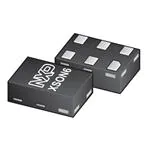
BGU8103X

BGU8103X

  • 厂商:

    NXP(恩智浦)

  • 封装:

    XFDFN6

  • 描述:

  • 详情介绍
  • 数据手册
  • 价格&库存
BGU8103X 数据手册
;6 21  BGU8103 SiGe:C low-noise amplifier MMIC for GPS, GLONASS, Galileo and COMPASS Rev. 3 — 18 January 2017 Product data sheet 1. General description The BGU8103 is, also known as the GPS1301M, an ultra low current and Low-Noise Amplifier (LNA) for GNSS receiver applications. The BGU8103 is available in a small plastic 6-pin extremely thin leadless package. The BGU8103 requires only one external matching inductor. The BGU8103 adapts itself to the changing environment resulting from co-habitation of different radio systems in modern cellular handsets. It has been designed for ultra low power consumption and optimal performance when jamming signals from co-existing cellular transmitters are present. At low jamming power levels, it delivers 17.5 dB gain at a noise figure of 0.80 dB and a supply current of 1.2 mA. During high jamming power levels, resulting for example from a cellular transmit burst, it temporarily increases its bias current to improve sensitivity. 2. Features and benefits                 Optimized performance at a low supply current of 1.2 mA Covers full GNSS L1 band, from 1559 MHz to 1610 MHz Noise figure = 0.80 dB Gain 17.5 dB Input 1 dB compression point of 16 dBm Out of band IP3i of 8 dBm Supply voltage 1.5 V to 3.1 V Self-shielding package concept Integrated supply decoupling capacitor Power-down mode current consumption < 1 A Integrated temperature stabilized bias for easy design Requires only one input matching inductor Integrated DC blocking at both RF input and output ESD protection on all pins (HBM > 2 kV) Integrated matching for the output Available in a 6-pin leadless package 1.1 mm  0.7 mm  0.37 mm; 0.4 mm pitch: SOT1232  180 GHz transit frequency - SiGe:C technology  Moisture sensitivity level 1 BGU8103 NXP Semiconductors SiGe:C LNA MMIC for GPS, GLONASS, Galileo and COMPASS 3. Applications         Smart phones Feature phones Tablets Digital still cameras Digital video cameras RF front-end modules Complete GNSS modules Personal health applications 4. Quick reference data Table 1. Quick reference data f = 1575 MHz; VCC = 1.8 V; VI(ENABLE)  0.8 V; Pi < 40 dBm; Tamb = 25 C; input matched to 50  using a 12 nH inductor; see Figure 3; unless otherwise specified. Symbol Parameter Conditions Min Typ Max Unit VCC supply voltage RF input AC coupled 1.5 - 3.1 V ICC supply current Pi < 40 dBm 0.8 1.2 1.6 mA Gp power gain no jammer 14.5 17.5 20.0 dB NF noise figure Pi = 40 dBm; no jammer - 0.8 1.4 dB [2] 19 16 - dBm [2][3] 11 8 - dBm Pi(1dB) input power at 1 dB gain compression IP3i input third-order intercept point [1] PCB losses are subtracted. [2] Guaranteed by device design; not tested in production. [3] f1 = 1713 MHz; f2 = 1851 MHz; Pi = 20 dBm at f1; Pi = 65 dBm at f2. [1][2] 5. Ordering information Table 2. Ordering information Type number Package Name Description Version BGU8103 XSON6 plastic extremely thin small outline package; no leads; 6 terminals; body 1.1  0.7  0.37 mm SOT1232 6. Marking Table 3. Marking codes Type number Marking code BGU8103 G BGU8103 Product data sheet All information provided in this document is subject to legal disclaimers. Rev. 3 — 18 January 2017 © NXP Semiconductors N.V. 2017. All rights reserved. 2 of 12 BGU8103 NXP Semiconductors SiGe:C LNA MMIC for GPS, GLONASS, Galileo and COMPASS 7. Block diagram 9&&  (1$%/( 5)B,1  %,$6&21752/   5)B287  DDD Fig 1. Block diagram 8. Pinning information 8.1 Pinning %*8 *1'B5)   5)B287 5)B,1   9&& (1$%/(   *1' 7UDQVSDUHQWWRSYLHZ DDD Fig 2. BGU8103 Product data sheet Pin configuration All information provided in this document is subject to legal disclaimers. Rev. 3 — 18 January 2017 © NXP Semiconductors N.V. 2017. All rights reserved. 3 of 12 BGU8103 NXP Semiconductors SiGe:C LNA MMIC for GPS, GLONASS, Galileo and COMPASS 8.2 Pin description Table 4. Pin description Symbol Pin Description GND 1 ground VCC 2 supply voltage RF_OUT 3 RF output GND_RF 4 ground RF RF_IN 5 RF input ENABLE 6 enable 9. Limiting values Table 5. Limiting values In accordance with the Absolute Maximum Rating System (IEC 60134). See Section 18.3 “Disclaimers”, paragraph “Limiting values”. Symbol Parameter Conditions supply voltage VCC VI(ENABLE) RF input AC coupled input voltage on pin ENABLE VI(ENABLE) < VCC + 0.6 V Min Max Unit [1] 0.5 +5.0 V [1][2] 0.5 +5.0 V 0.5 +5.0 V 0.5 +5.0 V - 10 dBm - 55 mW VI(RF_IN) input voltage on pin RF_IN DC; VI(RF_IN) < VCC + 0.6 V [1][2][3] VI(RF_OUT) input voltage on pin RF_OUT DC; VI(RF_OUT) < VCC + 0.6 V [1][2][3] Pi input power Ptot total power dissipation [1] Tsp  130 C Tstg storage temperature 65 +150 C Tj junction temperature - 150 C VESD electrostatic discharge voltage Human Body Model (HBM) according to JEDEC standard JS-001-2010 - 2 kV Charged Device Model (CDM) according to JEDEC standard JESD22-C101C - 2 kV [1] Stressed with pulses of 200 ms in duration, with application circuit as in Figure 3. [2] Warning: Due to internal ESD diode protection, to avoid excess current, the applied DC voltage must not exceed VCC + 0.6 V or 5.0 V. [3] The RF input and RF output are AC coupled through internal DC blocking capacitors. 10. Recommended operating conditions Table 6. Operating conditions Symbol Parameter VCC supply voltage 1.5 - Tamb ambient temperature 40 +25 +85 C VI(ENABLE) input voltage on pin ENABLE OFF state - - 0.3 V ON state 0.8 - - V BGU8103 Product data sheet Conditions All information provided in this document is subject to legal disclaimers. Rev. 3 — 18 January 2017 Min Typ Max Unit 3.1 V © NXP Semiconductors N.V. 2017. All rights reserved. 4 of 12 BGU8103 NXP Semiconductors SiGe:C LNA MMIC for GPS, GLONASS, Galileo and COMPASS 11. Thermal characteristics Table 7. Thermal characteristics Symbol Parameter Conditions Rth(j-sp) thermal resistance from junction to solder point Typ Unit 225 K/W 12. Characteristics Table 8. Characteristics at VCC = 1.8 V f = 1575 MHz; VCC = 1.8 V; VI(ENABLE)  0.8 V; Pi < 40 dBm; Tamb = 25 C; input matched to 50  using a 12 nH inductor; see Figure 3; unless otherwise specified. Symbol Parameter Conditions ICC supply current VI(ENABLE)  0.8 V power gain Gp RLin RLout input return loss output return loss ISL isolation NF noise figure Min Typ Max Unit Pi < 40 dBm 0.8 1.2 1.6 mA Pi = 20 dBm - 2.5 - mA - 1 A VI(ENABLE)  0.3 V - no jammer 14.5 17.5 20.0 dB Pjam = 20 dBm; fjam = 850 MHz - 18.5 - dB Pjam = 20 dBm; fjam = 1850 MHz - 18.0 - dB Pi < 40 dBm - 8 - dB Pi = 20 dBm - 9 - dB Pi < 40 dBm - 11 - dB Pi = 20 dBm - 11 - dB - 35 - dB Pi = 40 dBm; no jammer [1][2] - 0.8 1.4 dB Pi = 40 dBm; no jammer [2][3] - 0.9 1.5 dB Pjam = 20 dBm; fjam = 850 MHz [3] - 1.1 - dB Pjam = 20 dBm; fjam = 1850 MHz [3] - 1.4 - dB [2] 19 16 - dBm 11 8 - dBm - 72 - dBm Pi(1dB) input power at 1 dB gain compression IP3i input third-order intercept point IMD3 third-order intermodulation distortion output referred ton turn-on time time from VI(ENABLE) ON to 90 % of the gain - - 2 s toff turn-off time time from VI(ENABLE) OFF to 10 % of the gain - - 1 s [2][4] [1] PCB losses are subtracted. [2] Guaranteed by device design; not tested in production. [3] Including PCB losses. [4] f1 = 1713 MHz; f2 = 1851 MHz; Pi = 20 dBm at f1; Pi = 65 dBm at f2. BGU8103 Product data sheet All information provided in this document is subject to legal disclaimers. Rev. 3 — 18 January 2017 [4] © NXP Semiconductors N.V. 2017. All rights reserved. 5 of 12 BGU8103 NXP Semiconductors SiGe:C LNA MMIC for GPS, GLONASS, Galileo and COMPASS Table 9. Characteristics at VCC = 2.85 V f = 1575 MHz; VCC = 2.85 V; VI(ENABLE)  0.8 V; Pi < 40 dBm; Tamb = 25 C; input matched to 50  using a 12 nH inductor; see Figure 3; unless otherwise specified. Symbol Parameter Conditions ICC supply current VI(ENABLE)  0.8 V power gain Gp RLin RLout input return loss output return loss ISL isolation NF noise figure Min Typ Max Unit Pi < 40 dBm 0.8 1.2 1.6 mA Pi = 20 dBm - 2.5 - mA - 1 A VI(ENABLE)  0.3 V - no jammer 15.0 17.5 20.0 dB Pjam = 20 dBm; fjam = 850 MHz - 18.5 - dB Pjam = 20 dBm; fjam = 1850 MHz - 18.5 - dB Pi < 40 dBm - 8 - dB Pi = 20 dBm - 9 - dB Pi < 40 dBm - 11 - dB Pi = 20 dBm - 11 - dB - 35 - dB Pi = 40 dBm; no jammer [1][2] - 1.0 1.4 dB Pi = 40 dBm; no jammer [2][3] - 1.1 1.5 dB Pjam = 20 dBm; fjam = 850 MHz [3] - 1.1 - dB Pjam = 20 dBm; fjam = 1850 MHz [3] - 1.4 - dB [2] 16 13 - dBm 10 7 - dBm Pi(1dB) input power at 1 dB gain compression IP3i input third-order intercept point IMD3 third-order intermodulation distortion output referred ton turn-on time toff turn-off time [2][4] - 72 - dBm time from VI(ENABLE) ON to 90 % of the gain - - 2 s time from VI(ENABLE) OFF to 10 % of the gain - - 1 s [1] PCB losses are subtracted. [2] Guaranteed by device design; not tested in production. [3] Including PCB losses. [4] f1 = 1713 MHz; f2 = 1851 MHz; Pi = 20 dBm at f1; Pi = 65 dBm at f2. BGU8103 Product data sheet All information provided in this document is subject to legal disclaimers. Rev. 3 — 18 January 2017 [4] © NXP Semiconductors N.V. 2017. All rights reserved. 6 of 12 BGU8103 NXP Semiconductors SiGe:C LNA MMIC for GPS, GLONASS, Galileo and COMPASS 13. Application information 13.1 GNSS LNA 9HQ 9FF 5)LQ &  / 5)RXW    ,&   DDD For a list of components, see Table 10. Fig 3. Schematics GNSS LNA evaluation board Table 10. List of components For schematics, see Figure 3. BGU8103 Product data sheet Component Description Value Remarks C1 decoupling capacitor 1 nF to suppress power supply noise IC1 BGU8103 - NXP Semiconductors L1 high-quality matching inductor 12 nH Murata LQW15A All information provided in this document is subject to legal disclaimers. Rev. 3 — 18 January 2017 © NXP Semiconductors N.V. 2017. All rights reserved. 7 of 12 BGU8103 NXP Semiconductors SiGe:C LNA MMIC for GPS, GLONASS, Galileo and COMPASS 14. Package outline ;621SODVWLFH[WUHPHO\WKLQVPDOORXWOLQHSDFNDJHQROHDGVWHUPLQDOVERG\[[PP î $ ' 627 H   H ( Y H   $ % E î SLQ LQGH[DUHD SLQ LQGH[DUHD $ % \ Y $ % /  î \ & $ & î  PP VFDOH 'LPHQVLRQV PPDUHWKHRULJLQDOGLPHQVLRQV  8QLW PP $ $ ' ( PLQ    QRP    PD[     H H   E /       9 <
BGU8103X
物料型号:BGU8103,也被称作GPS1301M。

器件简介:该芯片是一款超低功耗的低噪声放大器(LNA),专为GNSS接收器应用设计。它能够适应现代手机中共存的不同无线系统所引起的环境变化。

引脚分配:共有6个引脚,包括地(GND)、供电电压(Vcc)、射频输出(RF_OUT)、射频输入(RFIN)和使能(ENABLE)。

参数特性: - 供电电压:1.5V至3.1V - 供电电流:在低干扰功率水平时为1.2mA - 增益:在无干扰时为17.5dB - 噪声系数:0.80dB - 输入1dB压缩点:-16dBm - 电源关闭模式下的电流消耗:<1μA

功能详解: - 该芯片优化了在1.2mA低供电电流下的效能。 - 覆盖了全GNSS L1频段,从1559MHz到1610MHz。 - 设计有自屏蔽封装概念和集成的电源解耦电容器。 - 所有引脚具有ESD保护功能(HBM > 2kV)。

应用信息:适用于智能手机、功能手机、平板电脑、数码相机、数字摄像机、射频前端模块、完整的GNSS模块和个人健康应用。

封装信息:BGU8103采用6引脚无引线超薄小外形封装,尺寸为1.1mm×0.7mm×0.37mm,引脚间距为0.4mm,型号为SOT1232。

BGU8103X 价格&库存

很抱歉,暂时无法提供与“BGU8103X”相匹配的价格&库存,您可以联系我们找货

免费人工找货