TO
-2
20F
BUJ302AX
NPN power transistor
Rev. 02 — 28 March 2011
Product data sheet
1. Product profile
1.1 General description
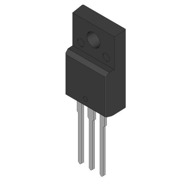
High-voltage, high-speed planar-passivated NPN power switching transistor in a
SOT186A (TO-220F) plastic package.
1.2 Features and benefits
Fast switching
Isolated package
High voltage capability
Low thermal resistance
1.3 Applications
DC-to-DC converters
Inverters
High-frequency electronic lighting
ballast applications
Motor control systems
1.4 Quick reference data
Table 1.
Quick reference data
Symbol
Parameter
Conditions
Min
Typ
Max Unit
IC
collector current
see Figure 1; see Figure 2;
see Figure 4
-
-
4
A
Ptot
total power
dissipation
Th ≤ 25 °C; see Figure 3
-
-
26
W
VCESM
collector-emitter
peak voltage
VBE = 0 V
-
-
1050 V
IC = 0.1 A; VCE = 5 V; Th = 25 °C;
see Figure 11
48
66
100
IC = 0.8 A; VCE = 3 V; Th = 25 °C;
see Figure 12
25
42
50
Static characteristics
hFE
DC current gain
�BUJ302AX
NXP Semiconductors
NPN power transistor
2. Pinning information
Table 2.
Pinning information
Pin
Symbol Description
1
B
base
2
C
collector
3
E
emitter
mb
n.c.
isolated
Simplified outline
Graphic symbol
mb
C
B
E
sym123
1 2 3
SOT186A (TO-220F)
3. Ordering information
Table 3.
Ordering information
Type number
Package
BUJ302AX
Name
Description
Version
TO-220F
plastic single-ended package; isolated heatsink mounted;
1 mounting hole; 3-lead TO-220 "full pack"
SOT186A
4. Limiting values
Table 4.
Limiting values
In accordance with the Absolute Maximum Rating System (IEC 60134).
Symbol
Parameter
Conditions
Min
Max
Unit
VCESM
collector-emitter peak voltage
VBE = 0 V
-
1050
V
VCEO
collector-emitter voltage
IB = 0 A
-
400
V
see Figure 1; see Figure 2; see Figure 4
-
4
A
-
8
A
-
2
A
-
4
A
IC
collector current
ICM
peak collector current
IB
base current
IBM
peak base current
DC
Th ≤ 25 °C; see Figure 3
Ptot
total power dissipation
-
26
W
Tstg
storage temperature
-65
150
°C
Tj
junction temperature
-
150
°C
VEBO
emitter-base voltage
-
24
V
BUJ302AX
Product data sheet
IC = 0 A; IE = 2 A; tp < 10 ms
All information provided in this document is subject to legal disclaimers.
Rev. 02 — 28 March 2011
© NXP B.V. 2011. All rights reserved.
2 of 13
�BUJ302AX
NXP Semiconductors
NPN power transistor
003aag027
10
VCC
IC
(A)
LC
VCL(CE)
probe point
8
LB
IBon
VBB
6
DUT
001aab999
4
2
0
0
Fig 1.
400
800
1200
VCEclamp (V)
Reverse bias safe operating area
Fig 2.
Test circuit for reverse bias safe operating area
03aa13
120
Pder
(%)
80
40
0
0
50
100
150
200
Th (°C)
Fig 3.
Normalized total power dissipation as a function of heatsink temperature
BUJ302AX
Product data sheet
All information provided in this document is subject to legal disclaimers.
Rev. 02 — 28 March 2011
© NXP B.V. 2011. All rights reserved.
3 of 13
�BUJ302AX
NXP Semiconductors
NPN power transistor
001aac001
102
IC
(A)
duty cycle = 0.01
10
ICM(max)
IC(max)
II(3)
(1)
1
(2)
10−1
tp = 20 μs
50 μs
100 μs
200 μs
500 μs
DC
I(3)
10−2
III(3)
10−3
102
10
1
103
VCEclamp (V)
1)Ptot maximum and Ptot peak maximum lines
2)Second breakdown limits
3) I = Region of permissable DC operation
II = Extension for repetitive pulse operation
III = Extension during turn-on in single transistor converters
provided that RBE ≤ 100 Ω and tp ≤ 0.6 μs
Fig 4.
Forward bias safe operating area for Tmb ≤ 25 °C
BUJ302AX
Product data sheet
All information provided in this document is subject to legal disclaimers.
Rev. 02 — 28 March 2011
© NXP B.V. 2011. All rights reserved.
4 of 13
�BUJ302AX
NXP Semiconductors
NPN power transistor
5. Thermal characteristics
Table 5.
Thermal characteristics
Symbol
Parameter
Conditions
Min
Typ
Max
Unit
Rth(j-h)
thermal resistance from
junction to heatsink
with heatsink compound; see Figure 5
-
-
4.8
K/W
Rth(j-a)
thermal resistance from
junction to ambient
in free air
-
55
-
K/W
001aag169
10
Zth(j-h)
(K/W)
1
10−1
10−2
δ = 0.5
0.2
0.1
0.05
0.02
δ=
P
0
t
tp
10−3
10−6 10−5 10−4 10−3 10−2 10−1
Fig 5.
tp
1/f
1/f
1
10 102
tp (s)
Transient thermal impedance from junction to heatsink as a function of pulse duration
6. Isolation characteristics
Table 6.
Isolation characteristics
Symbol
Parameter
Conditions
Min
Typ
Max
Unit
Visol(RMS)
RMS isolation voltage
50 Hz ≤ f ≤ 60 Hz; RH ≤ 65 %; Th = 25 °C;
from all terminals to external heatsink; clean
and dust free
-
-
2500
V
Cisol
isolation capacitance
from collector to external heatsink ; f = 1 MHz;
Th = 25 °C
-
10
-
pF
BUJ302AX
Product data sheet
All information provided in this document is subject to legal disclaimers.
Rev. 02 — 28 March 2011
© NXP B.V. 2011. All rights reserved.
5 of 13
�BUJ302AX
NXP Semiconductors
NPN power transistor
7. Characteristics
Table 7.
Characteristics
Symbol
Parameter
Conditions
Min
Typ
Max
Unit
Static characteristics
ICES
collector-emitter cut-off
current
VBE = 0 V; VCE = 1050 V; Tj = 25 °C
-
0.2
10
µA
ICEO
collector-emitter cut-off
current
VCE = 400 V; IB = 0 A; Th = 25 °C
-
10
250
µA
V(BR)EBO
open-collector emitter-base
breakdown voltage
IB = 1 mA; IC = 0 A; Th = 25 °C
15
19
-
V
VCEOsus
collector-emitter sustaining
voltage
IB = 0 A; IC = 10 mA; LC = 25 mH;
Th = 25 °C; see Figure 6; see Figure 7
400
470
-
V
VCEsat
collector-emitter saturation
voltage
IC = 1 A; IB = 0.2 A; Th = 25 °C;
see Figure 8; see Figure 9
-
0.15
0.5
V
IC = 3.5 A; IB = 1 A; Th = 25 °C;
see Figure 8; see Figure 9
-
0.6
1.5
V
V
VBEsat
base-emitter saturation
voltage
IC = 3.5 A; IB = 1 A; Th = 25 °C;
see Figure 10
-
1.1
1.5
hFE
DC current gain
IC = 0.1 A; VCE = 5 V; Th = 25 °C;
see Figure 11
48
66
100
IC = 0.8 A; VCE = 3 V; Th = 25 °C;
see Figure 12
25
42
50
IC = 2.5 A; IBon = 0.5 A; IBoff = -0.5 A;
RL = 60 Ω; VBB = -5 V; Th = 25 °C;
resistive load; tp = 300 µs;
see Figure 13; see Figure 14
-
-
3.5
µs
-
-
500
ns
Dynamic characteristics
ts
storage time
tf
fall time
IC
(mA)
50 V
100 Ω to 200 Ω
horizontal
oscilloscope
250
vertical
6V
300 Ω
1Ω
100
30 Hz to 60 Hz
001aab987
10
0
min
VCE (V)
VCEOsus
001aab988
Fig 6.
Test circuit for collector-emitter sustaining
voltage
BUJ302AX
Product data sheet
Fig 7.
Oscilloscope display for collector-emitter
sustaining voltage test waveform
All information provided in this document is subject to legal disclaimers.
Rev. 02 — 28 March 2011
© NXP B.V. 2011. All rights reserved.
6 of 13
�BUJ302AX
NXP Semiconductors
NPN power transistor
003aaf994
10
VCEsat
(V)
003aaf996
6
1.4 A
1.2 A
1.0 A
0.8 A
0.6 A
IC
(A)
4
1
0.4 A
Tj = 125 °C
IB = 0.2 A
10-1
10-2
10-2
2
Tj = 25 °C
10-1
0
1
0
10
2
4
6
8
IC (A)
Fig 8.
Collector-emitter saturation voltage as a
function of collector current; typical values
003aaf993
1.2
Fig 9.
10
VCE (V)
Collector current as a function of
collector-emitter voltage; typical values
003aaf992
102
VCE = 5 V
VBEsat
(V)
1.0
hFE
Tj = 25 °C
Tj = 25 °C
0.8
Tj = 125 °C
10
Tj = 125 °C
0.6
0.4
0.2
10-2
10-1
1
10
1
10-2
IC (A)
Product data sheet
1
10
IC (A)
Fig 10. Base-emitter saturation voltage as a function of
collector current; typical values
BUJ302AX
10-1
Fig 11. DC current gain as a function of collector
current; typical values
All information provided in this document is subject to legal disclaimers.
Rev. 02 — 28 March 2011
© NXP B.V. 2011. All rights reserved.
7 of 13
�BUJ302AX
NXP Semiconductors
NPN power transistor
003aaf991
102
VCC
VCE = 3 V
RL
hFE
VIM
0
Tj = 25 °C
Tj = 125 °C
RB
DUT
tp
T
10
1
10-2
001aab989
10-1
1
10
IC (A)
Fig 12. DC current gain as a function of collector
current; typical values
Fig 13. Test circuit for resistive load switching
IC
ICon
90 %
90 %
10 %
t
tf
ts
IB
ton
toff
IBon
10 %
t
tr ≤ 30 ns
−IBoff
001aab990
Fig 14. Switching times waveforms for resistive load
BUJ302AX
Product data sheet
All information provided in this document is subject to legal disclaimers.
Rev. 02 — 28 March 2011
© NXP B.V. 2011. All rights reserved.
8 of 13
�BUJ302AX
NXP Semiconductors
NPN power transistor
8. Package outline
Plastic single-ended package; isolated heatsink mounted;
1 mounting hole; 3-lead TO-220 'full pack'
SOT186A
E
A
A1
P
q
D1
mounting
base
T
D
j
L2
L1
K
Q
b1
L
b2
1
2
3
b
c
w M
e
e1
0
5
10 mm
scale
DIMENSIONS (mm are the original dimensions)
(1)
UNIT
A
A1
b
b1
b2
c
D
D1
E
e
e1
j
K
mm
4.6
4.0
2.9
2.5
0.9
0.7
1.1
0.9
1.4
1.0
0.7
0.4
15.8
15.2
6.5
6.3
10.3
9.7
2.54
5.08
2.7
1.7
0.6
0.4
L
L1
14.4 3.30
13.5 2.79
L2
max.
P
Q
q
3
3.2
3.0
2.6
2.3
3.0
2.6
T
(2)
2.5
w
0.4
Notes
1. Terminal dimensions within this zone are uncontrolled.
2. Both recesses are ∅ 2.5 × 0.8 max. depth
OUTLINE
VERSION
SOT186A
REFERENCES
IEC
JEDEC
JEITA
3-lead TO-220F
EUROPEAN
PROJECTION
ISSUE DATE
02-04-09
06-02-14
Fig 15. Package outline SOT186A (TO-220F)
BUJ302AX
Product data sheet
All information provided in this document is subject to legal disclaimers.
Rev. 02 — 28 March 2011
© NXP B.V. 2011. All rights reserved.
9 of 13
�BUJ302AX
NXP Semiconductors
NPN power transistor
9. Revision history
Table 8.
Revision history
Document ID
Release date
Data sheet status
Change notice
Supersedes
BUJ302AX v.2
20110328
Product data sheet
-
BUJ302AX v.1
Modifications:
BUJ302AX v.1
BUJ302AX
Product data sheet
•
The format of this data sheet has been redesigned to comply with the new identity guidelines
of NXP Semiconductors.
•
Legal texts have been adapted to the new company name where appropriate.
19980801
Objective specification
-
All information provided in this document is subject to legal disclaimers.
Rev. 02 — 28 March 2011
-
© NXP B.V. 2011. All rights reserved.
10 of 13
�BUJ302AX
NXP Semiconductors
NPN power transistor
10. Legal information
10.1 Data sheet status
Document status [1] [2]
Product status [3]
Definition
Objective [short] data sheet
Development
This document contains data from the objective specification for product development.
Preliminary [short] data sheet
Qualification
This document contains data from the preliminary specification.
Product [short] data sheet
Production
This document contains the product specification.
[1]
Please consult the most recently issued document before initiating or completing a design.
[2]
The term 'short data sheet' is explained in section "Definitions".
[3]
The product status of device(s) described in this document may have changed since this document was published and may differ in case of multiple devices. The latest product
status information is available on the Internet at URL http://www.nxp.com.
10.2 Definitions
Draft — The document is a draft version only. The content is still under
internal review and subject to formal approval, which may result in
modifications or additions. NXP Semiconductors does not give any
representations or warranties as to the accuracy or completeness of
information included herein and shall have no liability for the consequences of
use of such information.
Short data sheet — A short data sheet is an extract from a full data sheet
with the same product type number(s) and title. A short data sheet is intended
for quick reference only and should not be relied upon to contain detailed and
full information. For detailed and full information see the relevant full data
sheet, which is available on request via the local NXP Semiconductors sales
office. In case of any inconsistency or conflict with the short data sheet, the
full data sheet shall prevail.
Product specification — The information and data provided in a Product
data sheet shall define the specification of the product as agreed between
NXP Semiconductors and its customer, unless NXP Semiconductors and
customer have explicitly agreed otherwise in writing. In no event however,
shall an agreement be valid in which the NXP Semiconductors product is
deemed to offer functions and qualities beyond those described in the
Product data sheet.
10.3 Disclaimers
Limited warranty and liability — Information in this document is believed to
be accurate and reliable. However, NXP Semiconductors does not give any
representations or warranties, expressed or implied, as to the accuracy or
completeness of such information and shall have no liability for the
consequences of use of such information.
In no event shall NXP Semiconductors be liable for any indirect, incidental,
punitive, special or consequential damages (including - without limitation - lost
profits, lost savings, business interruption, costs related to the removal or
replacement of any products or rework charges) whether or not such
damages are based on tort (including negligence), warranty, breach of
contract or any other legal theory.
Suitability for use — NXP Semiconductors products are not designed,
authorized or warranted to be suitable for use in life support, life-critical or
safety-critical systems or equipment, nor in applications where failure or
malfunction of an NXP Semiconductors product can reasonably be expected
to result in personal injury, death or severe property or environmental
damage. NXP Semiconductors accepts no liability for inclusion and/or use of
NXP Semiconductors products in such equipment or applications and
therefore such inclusion and/or use is at the customer’s own risk.
Quick reference data — The Quick reference data is an extract of the
product data given in the Limiting values and Characteristics sections of this
document, and as such is not complete, exhaustive or legally binding.
Applications — Applications that are described herein for any of these
products are for illustrative purposes only. NXP Semiconductors makes no
representation or warranty that such applications will be suitable for the
specified use without further testing or modification.
Customers are responsible for the design and operation of their applications
and products using NXP Semiconductors products, and NXP Semiconductors
accepts no liability for any assistance with applications or customer product
design. It is customer’s sole responsibility to determine whether the NXP
Semiconductors product is suitable and fit for the customer’s applications and
products planned, as well as for the planned application and use of
customer’s third party customer(s). Customers should provide appropriate
design and operating safeguards to minimize the risks associated with their
applications and products.
NXP Semiconductors does not accept any liability related to any default,
damage, costs or problem which is based on any weakness or default in the
customer’s applications or products, or the application or use by customer’s
third party customer(s). Customer is responsible for doing all necessary
testing for the customer’s applications and products using NXP
Semiconductors products in order to avoid a default of the applications and
the products or of the application or use by customer’s third party
customer(s). NXP does not accept any liability in this respect.
Notwithstanding any damages that customer might incur for any reason
whatsoever, NXP Semiconductors’ aggregate and cumulative liability towards
customer for the products described herein shall be limited in accordance
with the Terms and conditions of commercial sale of NXP Semiconductors.
Limiting values — Stress above one or more limiting values (as defined in
the Absolute Maximum Ratings System of IEC 60134) will cause permanent
damage to the device. Limiting values are stress ratings only and (proper)
operation of the device at these or any other conditions above those given in
the Recommended operating conditions section (if present) or the
Characteristics sections of this document is not warranted. Constant or
repeated exposure to limiting values will permanently and irreversibly affect
the quality and reliability of the device.
Right to make changes — NXP Semiconductors reserves the right to make
changes to information published in this document, including without
limitation specifications and product descriptions, at any time and without
notice. This document supersedes and replaces all information supplied prior
to the publication hereof.
Terms and conditions of commercial sale — NXP Semiconductors
products are sold subject to the general terms and conditions of commercial
sale, as published at http://www.nxp.com/profile/terms, unless otherwise
agreed in a valid written individual agreement. In case an individual
agreement is concluded only the terms and conditions of the respective
BUJ302AX
Product data sheet
All information provided in this document is subject to legal disclaimers.
Rev. 02 — 28 March 2011
© NXP B.V. 2011. All rights reserved.
11 of 13
�BUJ302AX
NXP Semiconductors
NPN power transistor
agreement shall apply. NXP Semiconductors hereby expressly objects to
applying the customer’s general terms and conditions with regard to the
purchase of NXP Semiconductors products by customer.
No offer to sell or license — Nothing in this document may be interpreted or
construed as an offer to sell products that is open for acceptance or the grant,
conveyance or implication of any license under any copyrights, patents or
other industrial or intellectual property rights.
Export control — This document as well as the item(s) described herein may
be subject to export control regulations. Export might require a prior
authorization from national authorities.
Non-automotive qualified products — Unless this data sheet expressly
states that this specific NXP Semiconductors product is automotive qualified,
the product is not suitable for automotive use. It is neither qualified nor tested
in accordance with automotive testing or application requirements. NXP
Semiconductors accepts no liability for inclusion and/or use of
non-automotive qualified products in automotive equipment or applications.
In the event that customer uses the product for design-in and use in
automotive applications to automotive specifications and standards, customer
(a) shall use the product without NXP Semiconductors’ warranty of the
product for such automotive applications, use and specifications, and (b)
whenever customer uses the product for automotive applications beyond
NXP Semiconductors’ specifications such use shall be solely at customer’s
own risk, and (c) customer fully indemnifies NXP Semiconductors for any
liability, damages or failed product claims resulting from customer design and
use of the product for automotive applications beyond NXP Semiconductors’
standard warranty and NXP Semiconductors’ product specifications.
10.4 Trademarks
Notice: All referenced brands, product names, service names and trademarks
are the property of their respective owners.
Adelante, Bitport, Bitsound, CoolFlux, CoReUse, DESFire, EZ-HV,
FabKey, GreenChip, HiPerSmart, HITAG, I²C-bus logo, ICODE, I-CODE,
ITEC, Labelution, MIFARE, MIFARE Plus, MIFARE Ultralight, MoReUse,
QLPAK, Silicon Tuner, SiliconMAX, SmartXA, STARplug, TOPFET,
TrenchMOS, TriMedia and UCODE — are trademarks of NXP B.V.
HD Radio and HD Radio logo — are trademarks of iBiquity Digital
Corporation.
11. Contact information
For more information, please visit: http://www.nxp.com
For sales office addresses, please send an email to: salesaddresses@nxp.com
BUJ302AX
Product data sheet
All information provided in this document is subject to legal disclaimers.
Rev. 02 — 28 March 2011
© NXP B.V. 2011. All rights reserved.
12 of 13
�BUJ302AX
NXP Semiconductors
NPN power transistor
12. Contents
1
1.1
1.2
1.3
1.4
2
3
4
5
6
7
8
9
10
10.1
10.2
10.3
10.4
11
Product profile . . . . . . . . . . . . . . . . . . . . . . . . . . .1
General description . . . . . . . . . . . . . . . . . . . . . .1
Features and benefits . . . . . . . . . . . . . . . . . . . . .1
Applications . . . . . . . . . . . . . . . . . . . . . . . . . . . .1
Quick reference data . . . . . . . . . . . . . . . . . . . . .1
Pinning information . . . . . . . . . . . . . . . . . . . . . . .2
Ordering information . . . . . . . . . . . . . . . . . . . . . .2
Limiting values. . . . . . . . . . . . . . . . . . . . . . . . . . .2
Thermal characteristics . . . . . . . . . . . . . . . . . . .5
Isolation characteristics . . . . . . . . . . . . . . . . . . .5
Characteristics . . . . . . . . . . . . . . . . . . . . . . . . . . .6
Package outline . . . . . . . . . . . . . . . . . . . . . . . . . .9
Revision history . . . . . . . . . . . . . . . . . . . . . . . . .10
Legal information. . . . . . . . . . . . . . . . . . . . . . . . 11
Data sheet status . . . . . . . . . . . . . . . . . . . . . . . 11
Definitions . . . . . . . . . . . . . . . . . . . . . . . . . . . . . 11
Disclaimers . . . . . . . . . . . . . . . . . . . . . . . . . . . . 11
Trademarks. . . . . . . . . . . . . . . . . . . . . . . . . . . .12
Contact information. . . . . . . . . . . . . . . . . . . . . .12
Please be aware that important notices concerning this document and the product(s)
described herein, have been included in section ‘Legal information’.
© NXP B.V. 2011.
All rights reserved.
For more information, please visit: http://www.nxp.com
For sales office addresses, please send an email to: salesaddresses@nxp.com
Date of release: 28 March 2011
Document identifier: BUJ302AX
�