DISCRETE SEMICONDUCTORS
DATA SHEET
BYV42E, BYV42EB series
Rectifier diodes
ultrafast, rugged
Product specification
July 1998
�NXP Semiconductors
Product specification
Rectifier diodes
ultrafast, rugged
FEATURES
BYV42E, BYV42EB series
SYMBOL
• Low forward volt drop
• Fast switching
• Soft recovery characteristic
• Reverse surge capability
• High thermal cycling performance
• Low thermal resistance
QUICK REFERENCE DATA
VR = 150 V/ 200 V
VF ≤ 0.85 V
a2
3
a1
1
IO(AV) = 30 A
IRRM = 0.2 A
k 2
trr ≤ 28 ns
GENERAL DESCRIPTION
Dual, ultra-fast, epitaxial rectifier diodes intended for use as output rectifiers in high frequency switched mode power
supplies.
The BYV42E series is supplied in the SOT78 conventional leaded package.
The BYV42EB series is supplied in the SOT404 surface mounting package.
PINNING
PIN
SOT78 (TO220AB)
DESCRIPTION
1
anode 1 (a)
2
cathode (k) 1
3
anode 2 (a)
tab
cathode (k)
SOT404
tab
tab
2
1
1 23
3
LIMITING VALUES
Limiting values in accordance with the Absolute Maximum System (IEC 134).
SYMBOL
PARAMETER
VRRM
VRWM
VR
Peak repetitive reverse voltage
Crest working reverse voltage
Continuous reverse voltage
IO(AV)
Average rectified output current
(both diodes conducting)
Repetitive peak forward current
per diode
Non-repetitive peak forward
current per diode
CONDITIONS
MIN.
BYV42E / BYV42EB
IFRM
IFSM
IRRM
IRSM
Tstg
Tj
Tmb ≤ 144˚C
square wave
δ = 0.5; Tmb ≤ 108 ˚C
t = 25 µs; δ = 0.5;
Tmb ≤ 108 ˚C
t = 10 ms
t = 8.3 ms
sinusoidal; with reapplied
VRWM(max)
Repetitive peak reverse current tp = 2 µs; δ = 0.001
per diode
Non-repetitive peak reverse
tp = 100 µs
current per diode
Storage temperature
Operating junction temperature
-
MAX.
-150
150
150
150
UNIT
-200
200
200
200
V
V
V
-
30
A
-
30
A
-
150
160
A
A
-
0.2
A
-
0.2
A
-40
-
150
150
˚C
˚C
1. It is not possible to make connection to pin 2 of the SOT404 package
2. SOT78 package, For output currents in excess of 20 A, the cathode connection should be made to the mounting
tab.
July 1998
1
Rev 1.200
�NXP Semiconductors
Product specification
Rectifier diodes
ultrafast, rugged
BYV42E, BYV42EB series
ESD LIMITING VALUE
SYMBOL
PARAMETER
CONDITIONS
VC
Electrostatic discharge
capacitor voltage
Human body model;
C = 250 pF; R = 1.5 kΩ
MIN.
MAX.
UNIT
-
8
kV
THERMAL RESISTANCES
SYMBOL
PARAMETER
CONDITIONS
Rth j-mb
Thermal resistance junction to
mounting base
Thermal resistance junction to
ambient
per diode
both diodes
SOT78 package, in free air
SOT404 and SOT428 packages,
pcb mounted, minimum footprint,
FR4 board
Rth j-a
MIN.
TYP.
MAX.
UNIT
-
60
50
2.4
1.4
-
K/W
K/W
K/W
K/W
MIN.
TYP.
MAX.
UNIT
-
0.78
0.95
1.00
0.5
10
6
20
0.85
1.05
1.20
1
100
15
28
V
V
V
mA
µA
nC
ns
-
13
1
22
-
ns
V
ELECTRICAL CHARACTERISTICS
characteristics are per diode at Tj = 25 ˚C unless otherwise stated
SYMBOL
PARAMETER
CONDITIONS
VF
Forward voltage
IR
Reverse current
Qs
trr1
Reverse recovery charge
Reverse recovery time
trr2
Vfr
Reverse recovery time
Forward recovery voltage
IF = 15 A; Tj = 150˚C
IF = 15 A
IF = 30 A
VR = VRWM; Tj = 100 ˚C
VR = VRWM
IF = 2 A; VR ≥ 30 V; -dIF/dt = 20 A/µs
IF = 1 A; VR ≥ 30 V;
-dIF/dt = 100 A/µs
IF = 0.5 A to IR = 1 A; Irec = 0.25 A
IF = 1 A; dIF/dt = 10 A/µs
July 1998
2
Rev 1.200
�NXP Semiconductors
Product specification
Rectifier diodes
ultrafast, rugged
I
dI
F
BYV42E, BYV42EB series
0.5A
F
dt
IF
t
0A
rr
time
Q
I
10%
s
I rec = 0.25A
IR
100%
trr2
I
R
rrm
I = 1A
R
Fig.1. Definition of trr1, Qs and Irrm
I
Fig.4. Definition of trr2
20
F
PF / W
Tmb(max) / C
102
D = 1.0
BYV42
Vo = 0.705 V
Rs = 0.0097 Ohms
0.5
15
time
0.2
0.1
10
114
126
VF
V
tp
I
5
D=
tp
T
138
fr
t
T
VF
0
time
Fig.2. Definition of Vfr
0
5
10
15
IF(AV) / A
20
150
25
Fig.5. Maximum forward dissipation PF = f(IF(AV)) per
diode; square current waveform where
IF(AV) =IF(RMS) x √D.
R
15
PF / W
Tmb(max) / C
114
a = 1.57
BYV42
Vo = 0.705 V
Rs = 0.0097 Ohms
1.9
2.2
D.U.T.
2.8
10
Voltage Pulse Source
4
Current
shunt
138
5
to ’scope
0
0
5
IF(AV) / A
10
150
15
Fig.6. Maximum forward dissipation PF = f(IF(AV)) per
diode; sinusoidal current waveform where a = form
factor = IF(RMS) / IF(AV).
Fig.3. Circuit schematic for trr2
July 1998
126
3
Rev 1.200
�NXP Semiconductors
Product specification
Rectifier diodes
ultrafast, rugged
BYV42E, BYV42EB series
trr / ns
100 Qs / nC
1000
IF=20A
10A
5A
2A
1A
IF=20A
100
10
IF=1A
10
1
1
10
dIF/dt (A/us)
1.0
100
Fig.7. Maximum trr at Tj = 25 ˚C; per diode
10
-dIF/dt (A/us)
100
Fig.10. Maximum Qs at Tj = 25 ˚C; per diode
Irrm / A
10
1.0
10
Transient thermal impedance, Zth j-mb (K/W)
IF=20A
1
1
IF=1A
0.1
0.1
PD
0.01
0.001
1us
0.01
10
-dIF/dt (A/us)
1
100
Fig.8. Maximum Irrm at Tj = 25 ˚C; per diode
tp
D=
T
10us
tp
T
t
100us 1ms
10ms 100ms
1s
pulse width, tp (s)
BYV42E
10s
Fig.11. Transient thermal impedance; per diode;
Zth j-mb = f(tp).
IF / A
50
Tj = 150 C
40
Tj = 25 C
30
20
typ
10
max
0
0
0.5
VF / V
1.0
1.5
Fig.9. Typical and maximum forward characteristic
IF = f(VF); parameter Tj
July 1998
4
Rev 1.200
�NXP Semiconductors
Product specification
Rectifier diodes
ultrafast, rugged
BYV42E, BYV42EB series
MECHANICAL DATA
Dimensions in mm
4,5
max
Net Mass: 2 g
10,3
max
1,3
3,7
2,8
5,9
min
15,8
max
3,0 max
not tinned
3,0
13,5
min
1,3
max 1 2 3
(2x)
0,9 max (3x)
2,54 2,54
0,6
2,4
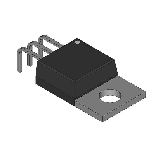
Fig.12. SOT78 (TO220AB); pin 2 connected to mounting base.
Notes
1. Refer to mounting instructions for SOT78 (TO220) envelopes.
2. Epoxy meets UL94 V0 at 1/8".
July 1998
5
Rev 1.200
�NXP Semiconductors
Product specification
Rectifier diodes
ultrafast, rugged
BYV42E, BYV42EB series
MECHANICAL DATA
Dimensions in mm
4.5 max
1.4 max
10.3 max
Net Mass: 1.4 g
11 max
15.4
2.5
0.85 max
(x2)
0.5
2.54 (x2)
Fig.13. SOT404 : centre pin connected to mounting base.
MOUNTING INSTRUCTIONS
Dimensions in mm
11.5
9.0
17.5
2.0
3.8
5.08
Fig.14. SOT404 : soldering pattern for surface mounting.
Notes
1. Epoxy meets UL94 V0 at 1/8".
July 1998
6
Rev 1.200
�NXP Semiconductors
Legal information
DATA SHEET STATUS
DOCUMENT
STATUS(1)
PRODUCT
STATUS(2)
DEFINITION
Objective data sheet
Development
This document contains data from the objective specification for product
development.
Preliminary data sheet
Qualification
This document contains data from the preliminary specification.
Product data sheet
Production
This document contains the product specification.
Notes
1. Please consult the most recently issued document before initiating or completing a design.
2. The product status of device(s) described in this document may have changed since this document was published
and may differ in case of multiple devices. The latest product status information is available on the Internet at
URL http://www.nxp.com.
DEFINITIONS
Product specification ⎯ The information and data
provided in a Product data sheet shall define the
specification of the product as agreed between NXP
Semiconductors and its customer, unless NXP
Semiconductors and customer have explicitly agreed
otherwise in writing. In no event however, shall an
agreement be valid in which the NXP Semiconductors
product is deemed to offer functions and qualities beyond
those described in the Product data sheet.
DISCLAIMERS
Limited warranty and liability ⎯ Information in this
document is believed to be accurate and reliable.
However, NXP Semiconductors does not give any
representations or warranties, expressed or implied, as to
the accuracy or completeness of such information and
shall have no liability for the consequences of use of such
information.
In no event shall NXP Semiconductors be liable for any
indirect, incidental, punitive, special or consequential
damages (including - without limitation - lost profits, lost
savings, business interruption, costs related to the
removal or replacement of any products or rework
charges) whether or not such damages are based on tort
(including negligence), warranty, breach of contract or any
other legal theory.
Notwithstanding any damages that customer might incur
for any reason whatsoever, NXP Semiconductors’
aggregate and cumulative liability towards customer for
the products described herein shall be limited in
accordance with the Terms and conditions of commercial
sale of NXP Semiconductors.
Right to make changes ⎯ NXP Semiconductors
reserves the right to make changes to information
published in this document, including without limitation
specifications and product descriptions, at any time and
without notice. This document supersedes and replaces all
information supplied prior to the publication hereof.
Suitability for use ⎯ NXP Semiconductors products are
not designed, authorized or warranted to be suitable for
use in life support, life-critical or safety-critical systems or
equipment, nor in applications where failure or malfunction
of an NXP Semiconductors product can reasonably be
expected to result in personal injury, death or severe
property or environmental damage. NXP Semiconductors
accepts no liability for inclusion and/or use of NXP
Semiconductors products in such equipment or
applications and therefore such inclusion and/or use is at
the customer’s own risk.
Applications ⎯ Applications that are described herein for
any of these products are for illustrative purposes only.
NXP Semiconductors makes no representation or
warranty that such applications will be suitable for the
specified use without further testing or modification.
Customers are responsible for the design and operation of
their applications and products using NXP
Semiconductors products, and NXP Semiconductors
accepts no liability for any assistance with applications or
customer product design. It is customer’s sole
responsibility to determine whether the NXP
Semiconductors product is suitable and fit for the
customer’s applications and products planned, as well as
for the planned application and use of customer’s third
party customer(s). Customers should provide appropriate
design and operating safeguards to minimize the risks
associated with their applications and products.
�NXP Semiconductors
Legal information
NXP Semiconductors does not accept any liability related
to any default, damage, costs or problem which is based
on any weakness or default in the customer’s applications
or products, or the application or use by customer’s third
party customer(s). Customer is responsible for doing all
necessary testing for the customer’s applications and
products using NXP Semiconductors products in order to
avoid a default of the applications and the products or of
the application or use by customer’s third party
customer(s). NXP does not accept any liability in this
respect.
Limiting values ⎯ Stress above one or more limiting
values (as defined in the Absolute Maximum Ratings
System of IEC 60134) will cause permanent damage to
the device. Limiting values are stress ratings only and
(proper) operation of the device at these or any other
conditions above those given in the Recommended
operating conditions section (if present) or the
Characteristics sections of this document is not warranted.
Constant or repeated exposure to limiting values will
permanently and irreversibly affect the quality and
reliability of the device.
Terms and conditions of commercial sale ⎯ NXP
Semiconductors products are sold subject to the general
terms and conditions of commercial sale, as published at
http://www.nxp.com/profile/terms, unless otherwise
agreed in a valid written individual agreement. In case an
individual agreement is concluded only the terms and
conditions of the respective agreement shall apply. NXP
Semiconductors hereby expressly objects to applying the
customer’s general terms and conditions with regard to the
purchase of NXP Semiconductors products by customer.
No offer to sell or license ⎯ Nothing in this document
may be interpreted or construed as an offer to sell products
that is open for acceptance or the grant, conveyance or
implication of any license under any copyrights, patents or
other industrial or intellectual property rights.
Export control ⎯ This document as well as the item(s)
described herein may be subject to export control
regulations. Export might require a prior authorization from
national authorities.
Quick reference data ⎯ The Quick reference data is an
extract of the product data given in the Limiting values and
Characteristics sections of this document, and as such is
not complete, exhaustive or legally binding.
Non-automotive qualified products ⎯ Unless this data
sheet expressly states that this specific NXP
Semiconductors product is automotive qualified, the
product is not suitable for automotive use. It is neither
qualified nor tested in accordance with automotive testing
or application requirements. NXP Semiconductors accepts
no liability for inclusion and/or use of non-automotive
qualified products in automotive equipment or
applications.
In the event that customer uses the product for design-in
and use in automotive applications to automotive
specifications and standards, customer (a) shall use the
product without NXP Semiconductors’ warranty of the
product for such automotive applications, use and
specifications, and (b) whenever customer uses the
product for automotive applications beyond NXP
Semiconductors’ specifications such use shall be solely at
customer’s own risk, and (c) customer fully indemnifies
NXP Semiconductors for any liability, damages or failed
product claims resulting from customer design and use of
the product for automotive applications beyond NXP
Semiconductors’ standard warranty and NXP
Semiconductors’ product specifications.
Customer notification
This data sheet was changed to reflect the new company name NXP Semiconductors, including new legal definitions
and disclaimers. No changes were made to the content, except for the legal definitions and disclaimers.
Contact information
For additional information please visit: http://www.nxp.com
For sales offices addresses send e-mail to: salesaddresses@nxp.com
© NXP B.V. 2011
All rights are reserved. Reproduction in whole or in part is prohibited without the prior written consent of the copyright owner.
The information presented in this document does not form part of any quotation or contract, is believed to be accurate and reliable and may be changed without
notice. No liability will be accepted by the publisher for any consequence of its use. Publication thereof does not convey nor imply any license under patent- or
other industrial or intellectual property rights.
Printed in The Netherlands
�