物料型号:BZV90系列
器件简介:
- 这些是中功率的电压调节二极管,采用SOT223塑料表面贴装封装。
- 该系列包含37种类型,工作电压范围为2.4至75伏(BZV90-C2V4至C75)。
- 这些二极管适用于一般调节功能。
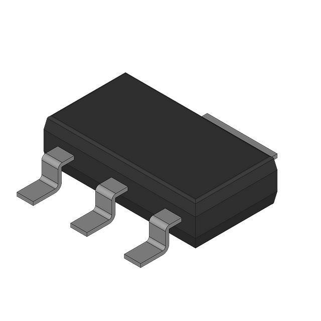
引脚分配:
- PIN 1: 阳极(anode)
- PIN 2: 阴极(cathode)
- PIN 3: 阳极(anode)
参数特性:
- 总功率消耗:最大1500毫瓦
- 公差系列:大约±5%
- 工作电压范围:名义值为2.4至75伏(E24范围)
- 非重复峰值反向功率消耗:最大40瓦
- 存储温度:-65至+150摄氏度
- 接点温度:最大150摄氏度
功能详解:
- 这些二极管在电路中提供电压调节功能,确保电路在规定的电压范围内稳定工作。
应用信息:
- 适用于一般调节功能,如电源电压稳定。
封装信息:
- 封装类型:SOT223
- 封装尺寸:具体尺寸数据以毫米为单位列出,包括长度、宽度和高度等。
电气特性:
- 连续正向电流(IF):最大400毫安
- 正向电压(VF):在50毫安测试电流下,典型值为1.0伏
热特性:
- 从结到环境的热阻(Rthj-a):83.3 K/W(在最大引线长度条件下)
图形数据:
- 提供了非重复峰值反向功率消耗与持续时间的关系图。
- 提供了正向电流与正向电压的关系图。
- 提供了工作电流与温度系数的关系图。
封装轮廓:
- 提供了SOT223封装的详细尺寸图。
文档状态:
- 该文档包含产品规格,是产品数据手册的一部分。
免责声明:
- NXP不对文档中的信息的准确性或完整性提供任何形式的保证。
- NXP保留随时更改文档中信息的权利。
联系信息:
- 提供了NXP公司的网址和销售办公室的电子邮件地址。
版权信息:
- 文档版权由NXP B.V.所有,未经版权所有者事先书面同意,禁止复制全部或部分内容。
发布日期:1999年5月17日
文档订单号:9397 750 05928