CLF1G0060-10; CLF1G0060S-10
Broadband RF power GaN HEMT
Rev. 2 — 29 January 2013
Objective data sheet
1. Product profile
1.1 General description
The CLF1G0060-10 and CLF1G0060S-10 are 10 W general purpose broadband GaN
HEMTs usable from DC to 6.0 GHz.
Table 1.
CW and pulsed RF application information
Typical RF performance at Tcase = 25 C; IDq = 40 mA; VDS = 50 V in a class-AB broadband demo
board.
Test signal
1-Tone CW
1-Tone pulsed
[1]
[1]
f
PL
Gp
D
(MHz)
(W)
(dB)
(%)
200
10
17.7
42.6
500
10
16.7
46.6
1000
10
15
38.7
1500
10
14.3
32.6
2000
10
14.2
32.6
200
10
18.8
44
500
10
17.8
48.2
1000
10
16.8
39
1500
10
16.7
33.9
2000
10
17
33.2
Pulsed RF; tp = 15 s; = 10 %.
Table 2.
2-Tone CW application information
Typical 2-Tone performance at Tcase = 25 C; IDq = 40 mA; VDS = 50 V in a class-AB broadband
demo board.
Test signal
2-Tone CW [1]
[1]
2-Tone CW; f = 1 MHz.
f
PL(PEP)
IMD3
(MHz)
(W)
(dBc)
500
5
47.4
1000
5
48.7
1500
5
44.7
2000
5
39.2
2500
5
40.4
�CLF1G0060-10; CLF1G0060S-10
NXP Semiconductors
Broadband RF power GaN HEMT
1.2 Features and benefits
Frequency of operation is from DC to 6.0 GHz
10 W general purpose broadband RF Power GaN HEMT
Excellent ruggedness (VSWR = 10 : 1)
High voltage operation (50 V)
Thermally enhanced package
1.3 Applications
Commercial wireless infrastructure
(cellular, WiMAX)
Radar
Broadband general purpose amplifier
Public mobile radios
Industrial, scientific, medical
Jammers
EMC testing
Defense application
2. Pinning information
Table 3.
Pinning
Pin
Description
Simplified outline
Graphic symbol
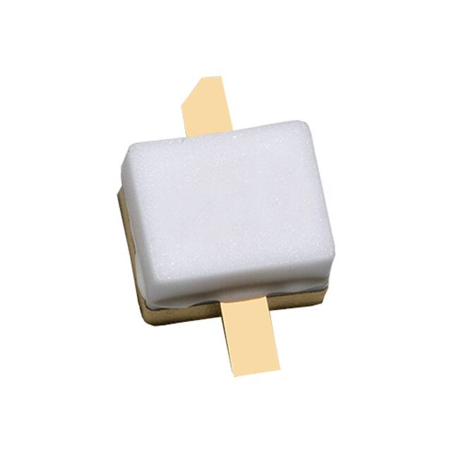
CLF1G0060-10 (SOT1227A)
1
drain
2
gate
3
source
�
�
�
[1]
�
�
�
DDD�������
CLF1G0060S-10 (SOT1227B)
1
drain
2
gate
3
source
�
�
�
[1]
�
�
[1]
DDD�������
Connected to flange.
3. Ordering information
Table 4.
Ordering information
Type number
CLF1G0060-10_1G0060S-10
Objective data sheet
Package
Name
Description
CLF1G0060-10
-
flanged ceramic package; 2 mounting holes; 2 leads SOT1227A
CLF1G0060S-10
-
earless flanged ceramic package; 2 leads
All information provided in this document is subject to legal disclaimers.
Rev. 2 — 29 January 2013
Version
SOT1227B
© NXP B.V. 2013. All rights reserved.
2 of 18
�CLF1G0060-10; CLF1G0060S-10
NXP Semiconductors
Broadband RF power GaN HEMT
4. Limiting values
Table 5.
Limiting values
In accordance with the Absolute Maximum Rating System (IEC 60134).
Symbol
Parameter
Conditions
VDS
drain-source voltage
VGS
gate-source voltage
IGF
forward gate current
Tstg
storage temperature
Tj
junction temperature
external RG = 5
measured via IR scan
Min
Max
Unit
-
150
V
8
+3
V
-
3.7
mA
65
+150
C
-
250
C
5. Thermal characteristics
Table 6.
Thermal characteristics
Symbol
Parameter
Conditions
Rth(j-c)
thermal resistance from junction to case
Tj = 200 C
[1]
[1]
Typ
Unit
K/W
Tj is measured via IR scan with case temperature of 85 C and power dissipation of W.
6. Characteristics
Table 7.
DC Characteristics
Tcase = 25 C; unless otherwise specified.
Symbol Parameter
Conditions
V(BR)DSS drain-source breakdown voltage VGS = 7 V;
IDS = 2.4 mA
Min
Typ
Max
Unit
150
-
-
V
VGS(th)
gate-source threshold voltage
VDS = 0.1 V;
IDS = 2.4 mA
2.4
2
1.6
V
IDSX
drain cut-off current
VDS = 10 V; VGS = 3 V
-
1.7
-
A
gfs
forward transconductance
VDS = 10 V; VGS = 0 V
-
0.38
-
S
Table 8.
RF Characteristics
Test signal: pulsed RF; tp = 100 s; = 10 %; RF performance at VDS = 50 V; IDq = 50 mA;
Tcase = 25 C; unless otherwise specified in a class-AB production circuit.
Symbol
Parameter
Conditions
f
frequency
D
drain efficiency
PL = 10 W
-
49.5
-
%
Gp
power gain
PL = 10 W
-
14.5
-
dB
RLin
input return loss
PL = 10 W
-
8.5
-
dB
PL = 10 W
-
0.04
-
dB
Pdroop(pulse) pulse droop power
CLF1G0060-10_1G0060S-10
Objective data sheet
Min
Typ
Max
Unit
3
-
3.5
GHz
tr
rise time
PL = 10 W
-
5
-
ns
tf
fall time
PL = 10 W
-
5
-
ns
All information provided in this document is subject to legal disclaimers.
Rev. 2 — 29 January 2013
© NXP B.V. 2013. All rights reserved.
3 of 18
�CLF1G0060-10; CLF1G0060S-10
NXP Semiconductors
Broadband RF power GaN HEMT
7. Application information
7.1 Demo circuit
&/)�*��������81,9(56$/�,1387��5(9��
5)���������&��&�
&/)�*��������81,9(56$/�287387��5(9��
5)���������&��&�
5�
&� &�
&�
&�
5�
&�
/�
&��
5�
&��
&��
&��
&��
&�
/�
&��
&��
&��
/�
&��
(�
&��
3�
*1'
6
9�
'
*
&
*1'
(
%
9*
*1'
)%
4�
4�
3�
3�
$�
3�
5�
&��
(�
DDD�������
Printed-Circuit Board (PCB) material: Taconic RF35, r = 3.5, thickness 30 mils, 1 oz copper on
each side.
See Table 9 for list of components.
Fig 1.
The broadband amplifier (500 MHz to 2500 MHz) demo circuit outline
Table 9.
List of components
See Figure 1.
CLF1G0060-10_1G0060S-10
Objective data sheet
Component Description
Value
Remarks
A1
GaN bias module v2
-
NXP
C1
multilayer ceramic chip capacitor 3.9 pF
ATC 600F
C2
multilayer ceramic chip capacitor 3.0 pF
ATC 600F
C3
multilayer ceramic chip capacitor 1.2 pF
ATC 600F
C4, C8
multilayer ceramic chip capacitor 33 pF
ATC 600F
C9
multilayer ceramic chip capacitor 10 pF
ATC 600F
C10
electrolytic capacitor
10 nF, 50 V
SMD 0805
C11
electrolytic capacitor
22 nF, 100 V
SMD 0805
C12
electrolytic capacitor
1 nF, 100 V
SMD 0805
All information provided in this document is subject to legal disclaimers.
Rev. 2 — 29 January 2013
© NXP B.V. 2013. All rights reserved.
4 of 18
�CLF1G0060-10; CLF1G0060S-10
NXP Semiconductors
Broadband RF power GaN HEMT
Table 9.
List of components …continued
See Figure 1.
CLF1G0060-10_1G0060S-10
Objective data sheet
Component Description
Value
Remarks
C13
electrolytic capacitor
100 nF, 50 V
SMD 0805
C20
multilayer ceramic chip capacitor 1 nF
ATC 700B
C21
multilayer ceramic chip capacitor 100 pF
ATC 700B
C22, C26
electrolytic capacitor
10 nF, 200 V
SMD 1210
C23
electrolytic capacitor
10 F, 100 V
SMD 2220
C25
electrolytic capacitor
1 F, 100 V
SMD 1206
Panasonic EEE-TK1J471AM
C27
electrolytic capacitor
470 F, 63 V
E1, E2
drain voltage connection
-
J1
RF in connector
-
J2
RF out connector
-
L1
inductor
100 nH
Coilcraft 0805CS-101XJL
L2
inductor
28 nH
Coilcraft B08TJL
L3
ferrite bead
5A
Fair-Rite 2743019447
P1, P2, P3,
P4
1 row, 4-way vertical DC
connector header
-
Q1
transistor
-
CLF1G0060-10
Q2
transistor
-
NXP BC857B
Q3
transistor
-
NXP PSMN8R2-80YS
R1
resistor
10.0
Generic
R2
resistor
10.0 k
Generic
R3
resistor
550
Generic
R4
resistor
0.01
Susumu RL7520WT-R010-F
All information provided in this document is subject to legal disclaimers.
Rev. 2 — 29 January 2013
© NXP B.V. 2013. All rights reserved.
5 of 18
�CLF1G0060-10; CLF1G0060S-10
NXP Semiconductors
Broadband RF power GaN HEMT
9'�,1
(�
$�
,1
�
�
�
�
'
*
6
9*
*$1�%,$6� �
02'8/( � )%
�
&
*1'
�
��
% �
4�
*1'
��
%&���%
�
(
��
�
*1'
�
�
�
�
�
�
�
�
&��
����)����9
5�
������ȍ
�
*1'
(�
4�
3601�5����
很抱歉,暂时无法提供与“CLF1G0060S-10U”相匹配的价格&库存,您可以联系我们找货
免费人工找货