Important notice
Dear Customer,
On 7 February 2017 the former NXP Standard Product business became a new company with the
tradename Nexperia. Nexperia is an industry leading supplier of Discrete, Logic and PowerMOS
semiconductors with its focus on the automotive, industrial, computing, consumer and wearable
application markets
In data sheets and application notes which still contain NXP or Philips Semiconductors references, use
the references to Nexperia, as shown below.
Instead of http://www.nxp.com, http://www.philips.com/ or http://www.semiconductors.philips.com/,
use http://www.nexperia.com
Instead of sales.addresses@www.nxp.com or sales.addresses@www.semiconductors.philips.com, use
salesaddresses@nexperia.com (email)
Replace the copyright notice at the bottom of each page or elsewhere in the document, depending on
the version, as shown below:
- © NXP N.V. (year). All rights reserved or © Koninklijke Philips Electronics N.V. (year). All rights
reserved
Should be replaced with:
- © Nexperia B.V. (year). All rights reserved.
If you have any questions related to the data sheet, please contact our nearest sales office via e-mail
or telephone (details via salesaddresses@nexperia.com). Thank you for your cooperation and
understanding,
Kind regards,
Team Nexperia
�INTEGRATED CIRCUITS
DATA SHEET
For a complete data sheet, please also download:
• The IC04 LOCMOS HE4000B Logic
Family Specifications HEF, HEC
• The IC04 LOCMOS HE4000B Logic
Package Outlines/Information HEF, HEC
HEF4016B
gates
Quadruple bilateral switches
Product specification
File under Integrated Circuits, IC04
January 1995
�Philips Semiconductors
Product specification
HEF4016B
gates
Quadruple bilateral switches
impedance between Y and Z is established (OFF
condition). Current through a switch will not cause
additional VDD current provided the voltage at the
terminals of the switch is maintained within the supply
voltage range; VDD ≥ (VY, VZ) ≥ VSS. Inputs Y and Z are
electrically equivalent terminals.
DESCRIPTION
The HEF4016B has four independent analogue switches
(transmission gates). Each switch has two input/output
terminals (Y/Z) and an active HIGH enable input (E). When
E is connected to VDD a low impedance bidirectional path
between Y and Z is established (ON condition). When E is
connected to VSS the switch is disabled and a high
Fig.2 Pinning diagram.
Fig.1 Functional diagram.
PINNING
E0 to E3
enable inputs
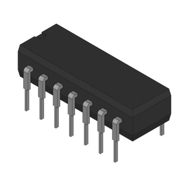
HEF4016BP(N): 14-lead DIL; plastic (SOT27-1)
Y0 to Y3
input/output terminals
HEF4016BD(F): 14-lead DIL; ceramic (cerdip) (SOT73)
Z0 to Z3
input/output terminals
HEF4016BT(D): 14-lead SO; plastic (SOT108-1)
( ): Package Designator North America
APPLICATION INFORMATION
Some examples of applications for the HEF4016B are:
• Signal gating
• Modulation
• Demodulation
• Chopper
Fig.3 Schematic diagram
(one switch).
January 1995
2
�Philips Semiconductors
Product specification
HEF4016B
gates
Quadruple bilateral switches
RATINGS
Limiting values in accordance with the Absolute Maximum System (IEC 134)
Power dissipation per switch
P
max.
100
mW
For other RATINGS see Family Specifications
DC CHARACTERISTICS
Tamb = 25 °C; VSS = 0 V (unless otherwise specified)
PARAMETER
VDD
V
SYMBOL
5
ON resistance
ON resistance
ON resistance
‘∆’ ON resistance
MAX.
UNIT
8000
−
Ω
230
690
Ω
15
115
350
Ω
5
140
425
Ω
10
RON
65
195
Ω
15
50
145
Ω
5
170
515
Ω
10
RON
95
285
Ω
15
75
220
Ω
5
200
−
Ω
15
−
Ω
10
−
Ω
10
between any two
10
channels
15
PARAMETER
TYP.
VDD
V
RON
∆RON
CONDITIONS
En at VIH; Vis = 0 to VDD; see Fig.4
En at VIH; Vis = VSS; see Fig.4
En at VIH; Vis = VDD; see Fig.4
En at VIH; Vis = 0 to VDD; see Fig.4
Tamb (°C)
−40
SYMBOL
+ 25
+ 85
UNIT
CONDITION
MIN. MAX. MIN. MAX. MIN. MAX.
Quiescent
5
device
10
current
15
Input leakage
current at En
OFF-state leakage
15
IDD
± IIN
5
−
1,0
−
1,0
−
7,5
µA
−
2,0
−
2,0
−
15,0
µA
−
4,0
−
4,0
−
30,0
µA
−
−
−
300
−
1000
−
−
−
−
−
−
nA
En at VSS or VDD
nA
En at VIL;
Vis = VSS or VDD;
Vos = VDD or VSS
current, any
10
−
−
−
−
−
−
nA
channel OFF
15
−
−
−
200
−
−
nA
5
−
1,5
−
1,5
−
1,5
V
En input
voltage LOW
En input
voltage HIGH
−
3,0
−
3,0
−
3,0
V
15
−
4,0
−
4,0
−
4,0
V
5
3,5
−
3,5
−
3,5
−
V
7,0
−
7,0
−
7,0
−
V
11,0
−
11,0
−
11,0
−
V
10
10
15
January 1995
IOZ
VIL
VIH
3
VSS = 0; all valid
input combinations;
VI = VSS or VDD
switch OFF; see
Fig.9 for IOZ
low-impedance
between Y and Z (ON
condition)
see RON switch
�Philips Semiconductors
Product specification
HEF4016B
gates
Quadruple bilateral switches
Fig.4 Test set-up for measuring RON.
En > VIH
Iis = 100 µA
VSS = 0 V
Fig.5 Typical RON as a function of input voltage.
January 1995
4
�Philips Semiconductors
Product specification
HEF4016B
gates
Quadruple bilateral switches
AC CHARACTERISTICS
VSS = 0 V; Tamb = 25 °C; input transition times ≤ 20 ns
VDD
V
SYMBOL
TYP.
MAX.
Propagation delays
Vis → Vos
HIGH to LOW
5
25
50
ns
10
20
ns
5
10
ns
20
40
ns
10
20
ns
15
5
10
ns
5
90
130
ns
80
110
ns
15
75
100
ns
5
85
120
ns
75
100
ns
15
75
100
ns
5
40
80
ns
20
40
ns
10
tPHL
15
5
LOW to HIGH
10
tPLH
note 1
note 1
Output disable times
En → Vos
HIGH
LOW
10
10
tPHZ
tPLZ
note 2
note 2
Output enable times
En → Vos
HIGH
LOW
Distortion, sine-wave
response
Crosstalk between
any two channels
Crosstalk; enable
input to output
OFF-state
feed-through
ON-state frequency
response
January 1995
10
tPZH
15
15
30
ns
5
40
80
ns
20
40
ns
15
15
30
5
−
%
10
0,08
%
15
0,04
5
−
MHz
10
1
MHz
10
tPZL
note 2
ns
note 3
%
15
−
MHz
5
−
mV
10
50
mV
15
−
mV
5
−
MHz
10
1
MHz
15
−
MHz
5
−
MHz
10
90
MHz
15
−
MHz
5
note 2
note 4
note 5
note 6
note 7
�Philips Semiconductors
Product specification
HEF4016B
gates
Quadruple bilateral switches
Notes
Vis is the input voltage at a Y or Z terminal, whichever is assigned as input.
Vos is the output voltage at a Y or Z terminal, whichever is assigned as output.
1. RL = 10 kΩ to VSS; CL = 50 pF to VSS; En = VDD; Vis = VDD (square-wave); see Figs 6 and 10.
2. RL = 10 kΩ; CL = 50 pF to VSS; En = VDD (square-wave);
Vis = VDD and RL to VSS for tPHZ and tPZH;
Vis = VSS and RL to VDD for tPLZ and tPZL; see Figs 6 and 11.
3. RL = 10 kΩ; CL = 15 pF; En = VDD; Vis = 1⁄2VDD(p-p) (sine-wave, symmetrical about 1⁄2VDD);
fis = 1 kHz; see Fig.7.
4. RL = 1 kΩ; Vis = 1⁄2VDD(p-p) (sine-wave, symmetrical about 1⁄2VDD);
V os (B)
20 log ------------------- = – 50 dB; E n (A) = V SS ; E n (B) = V DD ; see Fig. 8.
V is (A)
5. RL = 10 kΩ to VSS; CL = 15 pF to VSS; En = VDD (square-wave); crosstalk is Vos (peak value);
see Fig.6.
6. RL = 1 kΩ; CL = 5 pF; En = VSS; Vis = 1⁄2VDD(p-p) (sine-wave, symmetrical about 1⁄2VDD);
V os
20 log --------- = – 50 dB; see Fig. 7.
V is
7. RL = 1 kΩ; CL = 5 pF; En = VDD; Vis = 1⁄2VDD(p-p) (sine-wave, symmetrical about 1⁄2VDD);
V os
20 log --------- = – 3 dB; see Fig. 7.
V is
VDD
V
Dynamic power
dissipation per
package
(P)(1)
TYPICAL FORMULA FOR P (µW)
5
550 fi + ∑ (foCL) × VDD2
10
2 600 fi + ∑ (foCL) × VDD2
fi = input freq. (MHz)
15
6 500 fi + ∑ (foCL) × VDD
fo = output freq. (MHz)
2
where
CL = load capacitance (pF)
∑ (foCL) = sum of outputs
VDD = supply voltage (V)
Note
1. All enable inputs switching.
January 1995
6
�Philips Semiconductors
Product specification
HEF4016B
gates
Quadruple bilateral switches
Fig.6
Fig.7
Fig.8
Fig.9
January 1995
7
�Philips Semiconductors
Product specification
HEF4016B
gates
Quadruple bilateral switches
Fig.10 Waveforms showing propagation delays from Vis to Vos.
(1) Vis at VDD
(2) Vis at VSS
Fig.11 Waveforms showing output disable and enable times.
January 1995
8
�