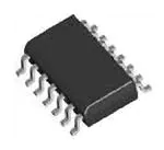
HTRC110
HITAG reader chip
Rev. 3.1 — 9 February 2010
037031
Product data sheet
PUBLIC
1. General description
The HITAG Reader Chip HTRC110 is intended for use with transponders, which are
based on NXP Semiconductors based HITAG transponder ICs.
In addition the IC supports other 125 kHz transponder types using amplitude modulation
for the write operation and AM/PM for the read operation. The receiver parameters (gain
factors, filter cutoff frequencies) can be optimized to system and transponder
requirements. The HTRC110 is designed for easy integration into RF-identification
readers. State-of-the-art technology allows almost complete integration of the necessary
building blocks. A powerful antenna driver/modulator together with a low-noise adaptive
sampling time demodulator, programmable filters/amplifier and digitizer build the complete
transceiver unit, required to design high-performance readers. A three-pin microcontroller
interface is employed for programming the HTRC110 as well as for the bidirectional
communication with the transponders. The three-wire interface can be changed into a
two-wire interface by connecting the data input and the data output.
Tolerance dependent zero amplitude modulation caused severe problems in envelope
detector systems, resulting in the need of very low tolerance reader antennas. These
problems are solved by the Adaptive Sampling Time technique (AST).
2. Features and benefits
Optimized for HITAG transponder ICs
Robust antenna coil power driver stage with modulator
High performance adaptive sampling time AM/PM demodulator (patent pending)
Read and write function
On-chip clock oscillator
Antenna rupture and short circuit detection
Low power consumption
Very low power stand-by mode
Low external component count
Small package (SO14)
3. Applications
Livestock tracking
Industrial applications
Logistics
�HTRC110
NXP Semiconductors
HITAG reader chip
4. Ordering information
Table 1.
Ordering information
Type number
Package
Name
Description
Version
HTRC11001T/02EE
SO14
plastic small outline package; 14 leads; body width 3.9 mm, tube
SOT108-1
HTRC11001T/03EE
SO14
plastic small outline package; 14 leads; body width 3.9 mm, reel
SOT108-1
5. Block diagram
Fig 1.
Block diagram HTRC110
037031
Product data sheet
PUBLIC
All information provided in this document is subject to legal disclaimers.
Rev. 3.1 — 9 February 2010
037031
© NXP B.V. 2010. All rights reserved.
2 of 22
�HTRC110
NXP Semiconductors
HITAG reader chip
6. Pinning information
6.1 Pinning
Fig 2.
Pin configuration
6.2 Pin description
Table 2.
037031
Product data sheet
PUBLIC
Pin description
Symbol
Pin
Description
VSS
1
GND, negative supply input
TX2
2
coil driver output
VDD
3
stabilized 5 V supply input
TX1
4
coil driver output
MODE
5
to enable filtering of SCLK and DIN (for active antenna applications)
XTAL1
6
oscillator interface, input
XTAL2
7
oscillator interface, output
SCLK
8
microcontroller interface: serial clock input
DIN
9
microcontroller interface: serial data in
DOUT
10
microcontroller interface: serial data out
n.c.
11
not connected
CEXT
12
high pass filter coupling
QGND
13
analog ground bias
RX
14
demodulator input
All information provided in this document is subject to legal disclaimers.
Rev. 3.1 — 9 February 2010
037031
© NXP B.V. 2010. All rights reserved.
3 of 22
�HTRC110
NXP Semiconductors
HITAG reader chip
7. Key data
Supply VDD:
5 V ± 10%
Clock/Osc. frequency:
4,8,12,16 MHz programmable
(antenna carrier frequency 125 kHz)
Antenna driver current:
200 mAp continuous
Serial interface:
CMOS compatible
Package:
SO14
Operation temperature range:
−40 °C to +85°C
8. Minimum application circuitry
The following figure shows a minimal application circuitry for the HTRC110. The reader
coil La together with the capacitor Ca forms a series resonant LC circuit (f = 125 kHz). The
high voltages in the LC circuit are divided to safe operating levels by Rv and the chip
internal resistor Rdem_in behind the RX-pin. The two capacitors connected to XTAL1 and
XTAL2 shall be the recommended values and types from the crystal's data sheet.
Alternatively to a crystal a ceramic resonator can be used or an external clock source can
be connected to XTAL1.
Fig 3.
037031
Product data sheet
PUBLIC
Minimum application circuitry
All information provided in this document is subject to legal disclaimers.
Rev. 3.1 — 9 February 2010
037031
© NXP B.V. 2010. All rights reserved.
4 of 22
�HTRC110
NXP Semiconductors
HITAG reader chip
9. Functional description
9.1 Power supply
The HTRC110 works with an external 5 V± 10 % power supply at VDD. The maximum
DC-current is 10 mA+Îant*2/ π = 137 mA. For optimum performance, the power supply
connection should be by-passed to ground with a 100 nF capacitor close to the IC.
9.2 Antenna driver, data input
The drivers deliver a square shaped voltage to the series resonant antenna circuit. Due to
the full bridge configuration of the drivers this voltage Udrvpp is approximately 10 V
(peak-peak) corresponding to Ûdrv = 5 V. The current flowing through the antenna is sine
shaped. It´s amplitude is approximately:
9.3 Diagnosis
In order to detect an antenna short or open condition the antenna tap voltage is
monitored. An antenna fail condition is reported in the status bit ANTFAIL (see Table 16),
if the antenna tap voltage does not go more negative than the diagnosis level DLEV (see
Table 18). This condition is checked for every coil driver cycle.
9.4 Oscillator/programmable divider/clock
The crystal oscillator at XTAL1/2 works with either crystal or ceramic resonators. It
delivers the input clock frequency of 4, 8, 12 or 16 MHz. The oscillator frequency is
divided by a programmable divider to obtain the carrier frequency of 125 kHz (see
Table 12). Alternatively, an external clock signal (CMOS compatible) may be fed into the
IC via XTAL1. For example, this signal can be derived from the microcontroller clock.
9.5 Adaptive sampling time demodulator
The demodulator senses the absorption modulation applied by a transponder when
inserted into the field. The signal is picked up at the antenna tap point between La and Ca.
It is divided by Rv and the internal resistor Rdem_in to a level below 8 V (peak) with respect
to QGND at the RX-pin (see Figure 3). Internally the signal is filtered with a second order
low pass filter.
The antenna current and therefore the tap voltage is modulated by the transponder in
amplitude and/or phase. This signal is fed into a synchronous demodulator recovering the
baseband signal. The amplification and the bandpass filter edge frequencies of the
demodulator can be adapted to different transponders via settings in the configuration
pages.
037031
Product data sheet
PUBLIC
All information provided in this document is subject to legal disclaimers.
Rev. 3.1 — 9 February 2010
037031
© NXP B.V. 2010. All rights reserved.
5 of 22
�HTRC110
NXP Semiconductors
HITAG reader chip
The phase between the driver excitation signal and the antenna tap voltage depends on
the antenna tuning. With optimum tuning, the phase of the antenna tap voltage is 90
degrees off the antenna driver signal. Detuning of the antenna resonant circuit results in a
change of this phase relationship.
The HTRC110's built-in phase measurement unit allows the measurement of this phase
relationship with a resolution of 360°/64 = 5.625°. This can be used to compute a
sampling time that compensates the mistuning of the reader antenna. The phase
measurement procedure can be carried out:
• either once before the first communication starts, if the position of the transponder
does not change with the respect to the reader antenna
• or during the communication (after sending the write pulses and before receiving the
answer of the transponder), if the tag is moving.
Before the system is switched into WRITE_TAG-mode, the demodulator has to be frozen.
This is internally done by clamping the input of the amplifier/filter unit to QGND. Doing so
avoids large transients in the amplifier and the digitizer, which could affect settling times.
In addition to the clamping, there exist other means in the HTRC110, which allow further
reduction of the settling times. All the parts of the circuitry, which are associated with these
functions, are controlled by the FREEZE0, FREEZE1 and THRESET bits, which are
located in configuration page 2.
For more details concerning WRITE Timing, Demodulator Setting, Power Up Sequence,
etc. please refer to the HTRC110 application note (Ref. 1).
9.6 Idle and power-down mode
The HTRC110 can be switched into idle mode via setting the PD-bit and resetting the
PD_MODE-bit. In this idle mode, only the oscillator and a few other system components
are active.
It is also possible to switch the IC completely off. This is achieved by the power-down
mode (PD = 1, PD_MODE = 1). Within this mode also the clock oscillator is switched off.
This reduces the supply current of the HTRC110 to less than 20 μA.
037031
Product data sheet
PUBLIC
All information provided in this document is subject to legal disclaimers.
Rev. 3.1 — 9 February 2010
037031
© NXP B.V. 2010. All rights reserved.
6 of 22
�HTRC110
NXP Semiconductors
HITAG reader chip
9.7 Serial interface
The communication between the HTRC110 and the microcontroller is done via a three
wire digital interface. The interface is operated by the following signals:
SCLK
DIN
DOUT
clock
data input
data output
SCLK and DIN are realized as Schmitt-Trigger inputs. DOUT is an open drain output with
internal pull-up resistor.
Every communication between HTRC110 and microcontroller begins with an initialization
of the serial interface. The interface initialization condition is a low-to-high transition of the
signal DIN while SCLK is high.
Fig 4.
Serial signaling
All commands are transmitted to the HTRC110 serial interface starting with Most
Significant Bit (MSB). DIN and DOUT are valid when SCLK is high.
9.8 Glitch filter for increased noise/interference immunity
Connecting pin 5 (MODE) to VDD enables digital filtering of the SCLK and the DIN input
signals. This mode offers improved immunity against glitches on these interface signals. It
is intended to be used in the so called "Active Antenna Applications" where the
microcontroller and the reader communicate via long signal lines (e.g. 1 meter).
In other applications pin 5 (MODE) has to be connected to GND.
Please refer to the HTRC110 application note (Ref. 1) for a detailed description of this
feature.
037031
Product data sheet
PUBLIC
All information provided in this document is subject to legal disclaimers.
Rev. 3.1 — 9 February 2010
037031
© NXP B.V. 2010. All rights reserved.
7 of 22
�HTRC110
NXP Semiconductors
HITAG reader chip
10. Commands
Table 3 depicts the HTRC110 command set summary.
Table 3.
HTRC110 commands
Bit No.
7
Command name
MSB
6
5
4
3
2
1
0
Remark
LSB
GET_SAMPLING_TIME
0
0
0
0
0
0
1
0
8 bit resp. (0 0 D5-D0)
GET_CONFIG_PAGE
0
0
0
0
0
1
P1
P0
8 bit resp. (X3-X0 D3-D0)
READ_PHASE
0
0
0
0
1
0
0
0
8 bit resp. (0 0 D5 - D0)
READ_TAG
1
1
1
-
-
-
-
-
READ_TAG-mode
WRITE_TAG_N
0
0
0
1
N3
N2
N0
N0
WRITE_TAG-mode with
pulse width programming
WRITE_TAG
1
1
0
-
-
-
-
-
WRITE_TAG-mode
SET_CONFIG_PAGE
0
1
P1
P0
D3
D2
D0
D0
4*4 config bits available
SET_SAMPLING_TIME
1
0
D5
D4
D3
D2
D0
D0
10.1 READ_TAG
This command is used to read the demodulated bit stream from a transponder: After the
assertion of the three command bits the HTRC110 instantaneously switches to
READ_TAG-mode and transmits the demodulated, filtered and digitized data from the
transponder. Data comes out and should be decoded by the microcontroller.
READ_TAG-mode is terminated by a low to high transition at SCLK.
Table 4.
Bit No.
READ_TAG command
7
6
5
4
3
2
1
0
Remark
Command 1
1
1
-
-
-
-
-
received data available at DOUT
10.2 WRITE_TAG_N
This command is used to write data to a transponder.
If N3 to N0 are set to zero, the signal from DIN is transparently switched to the drivers. A
high level at DIN corresponds to antenna drivers witched off, a low level corresponds to
antenna drivers switched on.
If any binary number between 1 and 1111 is loaded into N3 to N0 the drivers are switched
off at the next positive transition of DIN. This state is held for a time interval equal to N * T0
(T0 = 8 μs). This method relaxes the timing resolution requirements to the microcontroller
and to the software implementation while providing exact, selectable write pulse timing.
WRITE_TAG-mode is terminated immediately by a low to high transition at SCLK.
Table 5.
Bit No.
037031
Product data sheet
PUBLIC
READ_TAG_N command
7
6
5
4
3
2
1
0
Remark
Command 0
0
0
1
N3
N2
N1
N0
no response
All information provided in this document is subject to legal disclaimers.
Rev. 3.1 — 9 February 2010
037031
© NXP B.V. 2010. All rights reserved.
8 of 22
�HTRC110
NXP Semiconductors
HITAG reader chip
10.3 WRITE_TAG
This is the 3 bit short form of the previously described command WRITE_TAG_N. It allows
to switch into WRITE_TAG-mode with a minimum communication time.
The behaviour of the WRITE_TAG command is identical to WRITE_TAG_N with two
exceptions:
• WRITE_TAG-mode is entered after assertion of the 3rd command bit.
• No N parameter is specified with this command; instead the N value, which was
programmed with the most recent WRITE_TAG_N command, is used. If no
WRITE_TAG_N was issued so far, a default N = 0 (transparent mode) will be
assumed.
Table 6.
Bit No.
WRTIE_TAG command
7
6
5
4
3
2
1
0
Remark
Command 1
1
0
-
-
-
-
-
no response
10.4 READ_PHASE
This command is used to read the antenna´s phase, which is measured at every carrier
cycle. The phase is coded binary in D5 to D0.
Table 7.
Bit No.
READ_PHASE command
7
6
5
4
3
2
1
0
Remark
Command 0
0
0
0
1
0
0
0
-
Response
0
D5
D4
D3
D2
D1
D0
-
0
10.5 SET_SAMPLING_TIME
This command specifies the demodulator sampling time ts. The sampling time is coded
binary in D5 to D0.
Table 8.
Bit No.
SET_SAMPLING_TIME command
7
6
5
4
3
2
1
0
Remark
Command 1
0
D5
D4
D3
D2
D1
D0
no response
10.6 GET_SAMPLING_TIME
This command is used to read back the sampling time ts set with SET_SAMPLING_TIME.
The sampling time is coded binary in D5 to D0.
Table 9.
Bit No.
037031
Product data sheet
PUBLIC
GET_SAMPLING_TIME command
7
6
5
4
3
2
1
0
Remark
Command 0
0
0
0
0
0
1
0
-
Response
0
D5
D4
D3
D2
D1
D0
-
0
All information provided in this document is subject to legal disclaimers.
Rev. 3.1 — 9 February 2010
037031
© NXP B.V. 2010. All rights reserved.
9 of 22
�HTRC110
NXP Semiconductors
HITAG reader chip
10.7 SET_CONFIG_PAGE
This command is used to set the amplifier and filter parameters (cutoff frequencies, gain
factors) and the different operation modes. P1 and P0 select one of four configuration
pages.
Table 10.
SET_CONFIG_PAGE command
Bit No.
7
6
5
4
3
2
1
0
Remark
Command 0
1
P1
P0
D3
D2
01
D0
no response
Table 11.
Config pages
Bit No.
P1
P0
D3
D2
D1
D0
FILTERL
Command/Page no.
Table 12.
SET_CONFIG_PAGE 0
0
0
GAIN1
GAIN0
FILTERH
SET_CONFIG_PAGE 1
0
1
PD_MODE
PD
HYSTERESIS TXDIS
SET_CONFIG_PAGE 2
1
0
THRESET
ACQAMP
FREEZE1
FREEZ0
SET_CONFIG_PAGE 3
1
1
DIPSL1
DISSMARTCOMP
FSEL1
FSEL0
Bit initial conditions
Bit name
Description
Initial
condition
FILTERL
main low pass cutoff frequency
0
0: fL = 3 kHz
1: fL = 6 kHz
FILTERH
main high pass cutoff frequency
0
0: fH = 40 Hz
1: fH = 160 Hz
GAIN0
amplifier_0 gain factor
0
0: gain0 = 16; 1: gain0 = 32
GAIN1
amplifier_1 gain factor
1
0: gain1 = 6.22; 1: gain1 = 31.5
TXDIS
disable coil driver
0
0: coil driver active
1: coil driver inactive
HYSTERESIS
data comparator hysteresis
0
0: hysteresis OFF
1: hysteresis ON
PD
power down mode enable
0
0: device active
1: device power down
PD_MODE
select power down mode
0
0: idle mode
1: power down
FREEZE0
facility to achieve fast setting times
0
see Table 13
FREEZE1
facility to achieve fast setting times
0
see Table 13
ACQAMP
store signal amplitude as reference for later
amplitude comparison
0
see status bit AMPCOMP
THRESET
reset threshold generation of digitizer
0
FSEL0
clock frequency select LSB
0
00: 4 MHz, 01: 12 MHz
FSEL1
clock frequency select MSB
0
10: 8 MHz, 11: 16 MHz
DISSMARTCOMP
disable smart comparator
0
0: smart comparator = ON
1: smart comparator = OFF
DISPL1
disable low pass 1
0
0: low pass = ON
1: low pass = OFF
037031
Product data sheet
PUBLIC
All information provided in this document is subject to legal disclaimers.
Rev. 3.1 — 9 February 2010
037031
© NXP B.V. 2010. All rights reserved.
10 of 22
�HTRC110
NXP Semiconductors
HITAG reader chip
Table 13.
037031
Product data sheet
PUBLIC
Freeze bit description
FREEZE1
FREEZE0
Meaning
0
0
normal operation
0
1
main low pass is frozen; main high pass is precharged to QGND
1
0
main low pass is frozen; time constant of main high pass is reduced by
a factor of 16 for FILTERH=0 and by a factor 8 for FILTERH=1
1
1
time constant for main high pass is reduced by factor of 16 for
FILTERH=0 and by a factor of 8 for FILTERH=1; second high pass is
precharged
All information provided in this document is subject to legal disclaimers.
Rev. 3.1 — 9 February 2010
037031
© NXP B.V. 2010. All rights reserved.
11 of 22
�HTRC110
NXP Semiconductors
HITAG reader chip
10.8 GET_CONFIG_PAGE
This command has three functions:
1. Reading back the configuration parameters set by SET_CONFIG_PAGE command
2. Reading back the transmit pulse width programmed with WRITE_TAG_N
3. Reading the system status information
P1 and P0 select one of four configuration pages. The response (X3 X2 X1 X0 D3 D2 D1
D0) contains the contents of the selected configuration page in its lower nibble. For P = 0
or P = 1 the higher nibble reflects the current setting of N (the transmit pulse width). For
P = 2 or P = 3 the system status information is returned in the higher nibble.
Table 14.
Bit No.
GET_CONFIG_PAGE command
7
6
5
4
3
2
1
0
Command 0
0
0
0
0
1
P1
P0
Response
X2
X1
X0
D3
D2
D1
D0
Table 15.
X3
Remark
Config pages
Bit No.
7
6
5
4
3
2
1
0
GET_CONFIG_PAGE 0
N3
N2
N1
N0
D3
D2
D1
D0
GET_CONFIG_PAGE 1
N3
N2
N1
N0
D3
D2
D1
D0
GET_CONFIG_PAGE 2
0 (RFU)
0 (RFU)
AMPCOMP
ANTFAIL
D3
D2
D1
D0
GET_CONFIG_PAGE 3
0 (RFU)
0 (RFU)
AMPCOMP
ANTFAIL
D3
D2
D1
D0
Command/Page no.
Table 16.
Status bit description
Bit name
Meaning
ANTFAIL
antenna fail
AMPCOMP amplitude comparison
result
037031
Product data sheet
PUBLIC
0: antenna ok
1: antenna failure
When ACQAMP is set, the actual amplitude of the data
signal is stored as reference. After resetting ACQAMP
status bit AMPCOMP is set when the actual data signal
amplitude is higher than the stored reference.
All information provided in this document is subject to legal disclaimers.
Rev. 3.1 — 9 February 2010
037031
© NXP B.V. 2010. All rights reserved.
12 of 22
�HTRC110
NXP Semiconductors
HITAG reader chip
11. Limiting values
Table 17. Limiting values[1][2][3]
In accordance with the Absolute Maximum Rating System (IEC 60134).
Symbol
Parameter
Min
Max
Unit
voltage at any pin except RX
−0.3
+6.5
V
voltage at any pin except RX
−0.3
VDD + 0.3
V
voltage at RX pin
−10
+12
V
Tj
junction temperature
-
140
°C
Tstg
storage temperature
−65
+125
°C
[1]
Stresses above one or more of the limiting values may cause permanent damage to the device.
[2]
These are stress ratings only. Operation of the device at these or any other conditions above those given in
the characteristics section of the specification is not implied.
[3]
Exposure to limiting values for extended periods may affect device reliability.
12. Characteristics
Table 18. DC characteristics
VSS, Tamb = −40°C to +85 °C.
Symbol
Parameter
Conditions
Min
Typ
Max
Unit
4.5
5.0
5.5
V
Supply
VDD
supply voltage
IOn
operating supply current
VDD = 5.5 V, ITX1 = ITX2 = 0
Iid
idle current
VDD = 5.5 V
Ipd
power-down current
-
4
10
mA
-
0.2
0.4
mA
VDD = 5.5 V
-
7
20
μA
[1]
Drivers (TX1, TX2)
Iant
output peak-current
permanent
-
-
200
mAp
IantPulse
output peak-current
1:4 on/off-ratio ton