SO
8
KMZ49
Magnetic field sensor
Rev. 1 — 31 October 2011
Product data sheet
1. Product profile
1.1 General description
The KMZ49 is a sensitive magnetic field sensor, employing the magnetoresistive effect of
thin-film permalloy. The sensor contains two galvanic separated Wheatstone bridges, at a
relative angle of 45 to each other.
A rotating magnetic field in the x-y plane will produce two independent sinusoidal output
signals, one a function of +cos(2) and the second a function of +sin(2), being the
angle between sensor and field direction (see Figure 2). The KMZ49 is suited to high
precision angle measurement applications under low field conditions (saturation field
strength 25 kA/m).
The sensor can be operated at any frequency between 0 Hz and 1 MHz.
1.2 Features and benefits
Accurate and reliable angle measurement
Mechanical robustness, contactless principle
Wear-free operation
Accuracy independent of mechanical tolerances
Extended temperature range
1.3 Applications
Steering angle and torsion
Headlight adjustment
Motor positioning
Window wipers
Fuel level
Mirror positioning
�KMZ49
NXP Semiconductors
Magnetic field sensor
1.4 Quick reference data
Table 1.
Quick reference data
Tamb = 25 C; Hext = 25 kA/m; VCC = 5 V; unless otherwise specified.
Symbol
Parameter
Conditions
VCC
supply voltage
VM
peak voltage
[1]
see Figure 2
offset voltage
Voffset
per supply voltage;
see Figure 2
TCV(offset) offset voltage
temperature
coefficient
Rbridge
per supply voltage;
Tamb = 40 C to +150 C;
see Figure 2
bridge resistance
Min
Typ
Max
Unit
-
5
9
V
[1][2]
60
67
75
mV
[1]
2
-
+2
mV/V
[1][3]
2
-
+2
(V/V)/K
[1][4]
2.7
3.2
3.7
k
[1]
Applicable for bridge 1 and bridge 2.
[2]
VM = VO(max) Voffset. Periodicity of VM: sin(2) and cos(2), respectively.
[3]
V offset at 150 C – V offset at – 40 C
TC V offset = -------------------------------------------------------------------------------------------------150 C – – 40 C
[4]
Bridge resistance between pin 4 to pin 8, pin 3 to pin 7, pin 1 to pin 5 and pin 2 to pin 6.
2. Pinning information
Table 2.
Pinning
Pin
Symbol
Description
1
ON1
output voltage bridge 1
2
ON2
output voltage bridge 2
3
VCC2
supply voltage bridge 2
4
VCC1
supply voltage bridge 1
5
OP1
output voltage bridge 1
6
OP2
output voltage bridge 2
7
GND2
ground 2
8
GND1
ground 1
Simplified outline
8
5
1
4
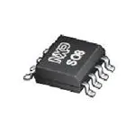
3. Ordering information
Table 3.
KMZ49
Product data sheet
Ordering information
Type number
Package
Name Description
Version
KMZ49
SO8
SOT96-1
plastic small outline package; 8 leads; body width 3.9 mm
All information provided in this document is subject to legal disclaimers.
Rev. 1 — 31 October 2011
© NXP B.V. 2011. All rights reserved.
2 of 13
�KMZ49
NXP Semiconductors
Magnetic field sensor
4. Circuit diagram
KMZ49
bridge 1
bridge 2
cos
R11
R13
VCC1
OP1
sin
R21
R12
R14
R22
R23
GND1
ON1
OP2
R24
GND2
VO1
VOP1
V
VCC2
VON2
VCC2
VO2
V
VCC1
ON2
V
VON1
V
VOP2
V
V
008aaa267
Fig 1.
Device and test circuit diagram
5. Limiting values
Table 4.
Limiting values
In accordance with the Absolute Maximum Rating System (IEC 60134).
Symbol
Parameter
VCC
supply voltage
Conditions
[1]
Min
Max
Unit
-
9
V
kA/m
Hext
external magnetic field strength
25
-
Tamb
ambient temperature
40
+150 C
Tstg
storage temperature
65
+150 C
[1]
Applicable for bridge 1 and bridge 2.
6. Thermal characteristics
Table 5.
KMZ49
Product data sheet
Thermal characteristics
Symbol
Parameter
Typ
Unit
Rth(j-a)
thermal resistance from junction to ambient
155
K/W
All information provided in this document is subject to legal disclaimers.
© NXP B.V. 2011. All rights reserved.
Rev. 1 — 31 October 2011
Conditions
3 of 13
�KMZ49
NXP Semiconductors
Magnetic field sensor
7. Characteristics
Table 6.
Characteristics
Tamb = 25 C; Hext = 25 kA/m; VCC = 5 V; unless otherwise specified.
Symbol
Parameter
Conditions
[1]
Min
Typ
Max
Unit
VCC
supply voltage
-
5
9
V
VM
peak voltage
see Figure 2
[1][2]
60
67
75
mV
TCVM
peak voltage temperature
coefficient
Tamb = 40 C to +150 C
[1][3]
0.3
0.36
0.42
%/K
Rbridge
bridge resistance
[1][4]
2.7
3.2
3.7
k
TCR(bridge)
bridge resistance
temperature coefficient
Tamb = 40 C to +150 C
[1][5]
0.24
0.26
0.29
%/K
Voffset
offset voltage
per supply voltage;
see Figure 2
[1]
2
-
+2
mV/V
TCV(offset)
offset voltage temperature
coefficient
per supply voltage;
Tamb = 40 C to +150 C;
see Figure 2
[1][6]
2
-
+2
(V/V)/K
Vo(hys)
hysteresis output voltage
see Figure 3
[1][7]
k
amplitude synchronism
TCk
amplitude synchronism
temperature coefficient
angular inaccuracy
Tamb = 40 C to +150 C
0
0.05
0.18
%FS
[8]
99.5
100
100.5
%
[9]
0.01
0
+0.01
%/K
0
0.05
0.1
deg
[10]
[1]
Applicable for bridge 1 and bridge 2.
[2]
VM = VO(max) Voffset. Periodicity of VM: sin(2) and cos(2), respectively.
[3]
V M at 150 C – V M at – 40 C
TCVM = --------------------------------------------------------------------------------------------V M at 25 C 150 C – – 40 C
[4]
Bridge resistance between pin 4 to pin 8, pin 3 to pin 7, pin 1 to pin 5 and pin 2 to pin 6.
[5]
R bridge at 150 C – R bridge at – 40 C
TCR bridge = ------------------------------------------------------------------------------------------------------R bridge at 25 C 150 C – – 40 C
[6]
V offset at 150 C – V offset at – 40 C
TCV offset = -------------------------------------------------------------------------------------------------150 C – – 40 C
[7]
V O1 67.5 135 45 – V O1 67.5 45 135
V o hys 1 = --------------------------------------------------------------------------------------------------------------------------2 V M1
V O2 22.5 90 0 – V O2 22.5 0 90
V o hys 2 = --------------------------------------------------------------------------------------------------------------2 V M2
[8]
V M1
k = ---------V M2
[9]
k at 150 C – k at – 40 C
TCk = ---------------------------------------------------------------------------------------k at 25 C 150 C – – 40 C
[10] = real – meas ; Voffset = 0 V; inaccuracy of angular measurement due to deviations from ideal sinusoidal characteristics,
calculated from the third and fifth harmonics of the spectrum VO. For definition of see Figure 2.
KMZ49
Product data sheet
All information provided in this document is subject to legal disclaimers.
Rev. 1 — 31 October 2011
© NXP B.V. 2011. All rights reserved.
4 of 13
�KMZ49
NXP Semiconductors
Magnetic field sensor
VO
(mV)
α = 0°
VO2
direction of
magnetic field
α
VM2
Voffset2
ON1
GND1
ON2
GND2
0
VCC2
OP2
VCC1
OP1
VO1
0
90
180
270
α (deg)
360
008aaa269
Fig 2.
Output signals related to the direction of the magnetic field
008aaa266
VO
(mV)
Vo(hys)2
VO1
0
VO2
Vo(hys)1
0
Fig 3.
KMZ49
Product data sheet
45
90
α (deg)
135
Definition of hysteresis
All information provided in this document is subject to legal disclaimers.
Rev. 1 — 31 October 2011
© NXP B.V. 2011. All rights reserved.
5 of 13
�KMZ49
NXP Semiconductors
Magnetic field sensor
8. ElectroStatic Discharge (ESD)
8.1 Human body model
The KMZ49 withstands 1 kV, according to the human body model at 100 pF and 1.5 k.
The test is according to AEC-Q101, method 001.
9. Test information
9.1 Quality information
This product has been qualified in accordance with the Automotive Electronics Council
(AEC) standard Q101 - Stress test qualification for discrete semiconductors, and is
suitable for use in automotive applications.
KMZ49
Product data sheet
All information provided in this document is subject to legal disclaimers.
Rev. 1 — 31 October 2011
© NXP B.V. 2011. All rights reserved.
6 of 13
�KMZ49
NXP Semiconductors
Magnetic field sensor
10. Package outline
SO8: plastic small outline package; 8 leads; body width 3.9 mm
SOT96-1
D
E
A
X
c
y
HE
v M A
Z
5
8
Q
A2
A
(A 3)
A1
pin 1 index
θ
Lp
1
L
4
e
detail X
w M
bp
0
2.5
5 mm
scale
DIMENSIONS (inch dimensions are derived from the original mm dimensions)
UNIT
A
max.
A1
A2
A3
bp
c
D (1)
E (2)
e
HE
L
Lp
Q
v
w
y
Z (1)
mm
1.75
0.25
0.10
1.45
1.25
0.25
0.49
0.36
0.25
0.19
5.0
4.8
4.0
3.8
1.27
6.2
5.8
1.05
1.0
0.4
0.7
0.6
0.25
0.25
0.1
0.7
0.3
0.01
0.019 0.0100
0.014 0.0075
0.20
0.19
0.16
0.15
inches
0.010 0.057
0.069
0.004 0.049
0.05
0.244
0.039 0.028
0.041
0.228
0.016 0.024
0.01
0.01
0.028
0.004
0.012
θ
8o
o
0
Notes
1. Plastic or metal protrusions of 0.15 mm (0.006 inch) maximum per side are not included.
2. Plastic or metal protrusions of 0.25 mm (0.01 inch) maximum per side are not included.
Fig 4.
REFERENCES
OUTLINE
VERSION
IEC
JEDEC
SOT96-1
076E03
MS-012
JEITA
EUROPEAN
PROJECTION
ISSUE DATE
99-12-27
03-02-18
Package outline SOT96-1 (SO8)
KMZ49
Product data sheet
All information provided in this document is subject to legal disclaimers.
Rev. 1 — 31 October 2011
© NXP B.V. 2011. All rights reserved.
7 of 13
�KMZ49
NXP Semiconductors
Magnetic field sensor
11. Soldering of SMD packages
This text provides a very brief insight into a complex technology. A more in-depth account
of soldering ICs can be found in Application Note AN10365 “Surface mount reflow
soldering description”.
11.1 Introduction to soldering
Soldering is one of the most common methods through which packages are attached to
Printed Circuit Boards (PCBs), to form electrical circuits. The soldered joint provides both
the mechanical and the electrical connection. There is no single soldering method that is
ideal for all IC packages. Wave soldering is often preferred when through-hole and
Surface Mount Devices (SMDs) are mixed on one printed wiring board; however, it is not
suitable for fine pitch SMDs. Reflow soldering is ideal for the small pitches and high
densities that come with increased miniaturization.
11.2 Wave and reflow soldering
Wave soldering is a joining technology in which the joints are made by solder coming from
a standing wave of liquid solder. The wave soldering process is suitable for the following:
• Through-hole components
• Leaded or leadless SMDs, which are glued to the surface of the printed circuit board
Not all SMDs can be wave soldered. Packages with solder balls, and some leadless
packages which have solder lands underneath the body, cannot be wave soldered. Also,
leaded SMDs with leads having a pitch smaller than ~0.6 mm cannot be wave soldered,
due to an increased probability of bridging.
The reflow soldering process involves applying solder paste to a board, followed by
component placement and exposure to a temperature profile. Leaded packages,
packages with solder balls, and leadless packages are all reflow solderable.
Key characteristics in both wave and reflow soldering are:
•
•
•
•
•
•
Board specifications, including the board finish, solder masks and vias
Package footprints, including solder thieves and orientation
The moisture sensitivity level of the packages
Package placement
Inspection and repair
Lead-free soldering versus SnPb soldering
11.3 Wave soldering
Key characteristics in wave soldering are:
• Process issues, such as application of adhesive and flux, clinching of leads, board
transport, the solder wave parameters, and the time during which components are
exposed to the wave
• Solder bath specifications, including temperature and impurities
KMZ49
Product data sheet
All information provided in this document is subject to legal disclaimers.
Rev. 1 — 31 October 2011
© NXP B.V. 2011. All rights reserved.
8 of 13
�KMZ49
NXP Semiconductors
Magnetic field sensor
11.4 Reflow soldering
Key characteristics in reflow soldering are:
• Lead-free versus SnPb soldering; note that a lead-free reflow process usually leads to
higher minimum peak temperatures (see Figure 5) than a SnPb process, thus
reducing the process window
• Solder paste printing issues including smearing, release, and adjusting the process
window for a mix of large and small components on one board
• Reflow temperature profile; this profile includes preheat, reflow (in which the board is
heated to the peak temperature) and cooling down. It is imperative that the peak
temperature is high enough for the solder to make reliable solder joints (a solder paste
characteristic). In addition, the peak temperature must be low enough that the
packages and/or boards are not damaged. The peak temperature of the package
depends on package thickness and volume and is classified in accordance with
Table 7 and 8
Table 7.
SnPb eutectic process (from J-STD-020C)
Package thickness (mm)
Package reflow temperature (C)
Volume (mm3)
< 350
350
< 2.5
235
220
2.5
220
220
Table 8.
Lead-free process (from J-STD-020C)
Package thickness (mm)
Package reflow temperature (C)
Volume (mm3)
< 350
350 to 2000
> 2000
< 1.6
260
260
260
1.6 to 2.5
260
250
245
> 2.5
250
245
245
Moisture sensitivity precautions, as indicated on the packing, must be respected at all
times.
Studies have shown that small packages reach higher temperatures during reflow
soldering, see Figure 5.
KMZ49
Product data sheet
All information provided in this document is subject to legal disclaimers.
Rev. 1 — 31 October 2011
© NXP B.V. 2011. All rights reserved.
9 of 13
�KMZ49
NXP Semiconductors
Magnetic field sensor
temperature
maximum peak temperature
= MSL limit, damage level
minimum peak temperature
= minimum soldering temperature
peak
temperature
time
001aac844
MSL: Moisture Sensitivity Level
Fig 5.
Temperature profiles for large and small components
For further information on temperature profiles, refer to Application Note AN10365
“Surface mount reflow soldering description”.
12. Revision history
Table 9.
Revision history
Document ID
Release date
Data sheet status
Change notice
Supersedes
KMZ49 v.1
20111031
Product data sheet
-
-
KMZ49
Product data sheet
All information provided in this document is subject to legal disclaimers.
Rev. 1 — 31 October 2011
© NXP B.V. 2011. All rights reserved.
10 of 13
�KMZ49
NXP Semiconductors
Magnetic field sensor
13. Legal information
13.1 Data sheet status
Document status[1][2]
Product status[3]
Objective [short] data sheet
Development
This document contains data from the objective specification for product development.
Preliminary [short] data sheet
Qualification
This document contains data from the preliminary specification.
Product [short] data sheet
Production
This document contains the product specification.
Definition
[1]
Please consult the most recently issued document before initiating or completing a design.
[2]
The term ‘short data sheet’ is explained in section “Definitions”.
[3]
The product status of device(s) described in this document may have changed since this document was published and may differ in case of multiple devices. The latest product status
information is available on the Internet at URL http://www.nxp.com.
13.2 Definitions
Draft — The document is a draft version only. The content is still under
internal review and subject to formal approval, which may result in
modifications or additions. NXP Semiconductors does not give any
representations or warranties as to the accuracy or completeness of
information included herein and shall have no liability for the consequences of
use of such information.
Short data sheet — A short data sheet is an extract from a full data sheet
with the same product type number(s) and title. A short data sheet is intended
for quick reference only and should not be relied upon to contain detailed and
full information. For detailed and full information see the relevant full data
sheet, which is available on request via the local NXP Semiconductors sales
office. In case of any inconsistency or conflict with the short data sheet, the
full data sheet shall prevail.
Product specification — The information and data provided in a Product
data sheet shall define the specification of the product as agreed between
NXP Semiconductors and its customer, unless NXP Semiconductors and
customer have explicitly agreed otherwise in writing. In no event however,
shall an agreement be valid in which the NXP Semiconductors product is
deemed to offer functions and qualities beyond those described in the
Product data sheet.
13.3 Disclaimers
Limited warranty and liability — Information in this document is believed to
be accurate and reliable. However, NXP Semiconductors does not give any
representations or warranties, expressed or implied, as to the accuracy or
completeness of such information and shall have no liability for the
consequences of use of such information.
In no event shall NXP Semiconductors be liable for any indirect, incidental,
punitive, special or consequential damages (including - without limitation - lost
profits, lost savings, business interruption, costs related to the removal or
replacement of any products or rework charges) whether or not such
damages are based on tort (including negligence), warranty, breach of
contract or any other legal theory.
Notwithstanding any damages that customer might incur for any reason
whatsoever, NXP Semiconductors’ aggregate and cumulative liability towards
customer for the products described herein shall be limited in accordance
with the Terms and conditions of commercial sale of NXP Semiconductors.
Right to make changes — NXP Semiconductors reserves the right to make
changes to information published in this document, including without
limitation specifications and product descriptions, at any time and without
notice. This document supersedes and replaces all information supplied prior
to the publication hereof.
Suitability for use in automotive applications — This NXP
Semiconductors product has been qualified for use in automotive
applications. Unless otherwise agreed in writing, the product is not designed,
KMZ49
Product data sheet
authorized or warranted to be suitable for use in life support, life-critical or
safety-critical systems or equipment, nor in applications where failure or
malfunction of an NXP Semiconductors product can reasonably be expected
to result in personal injury, death or severe property or environmental
damage. NXP Semiconductors accepts no liability for inclusion and/or use of
NXP Semiconductors products in such equipment or applications and
therefore such inclusion and/or use is at the customer's own risk.
Applications — Applications that are described herein for any of these
products are for illustrative purposes only. NXP Semiconductors makes no
representation or warranty that such applications will be suitable for the
specified use without further testing or modification.
Customers are responsible for the design and operation of their applications
and products using NXP Semiconductors products, and NXP Semiconductors
accepts no liability for any assistance with applications or customer product
design. It is customer’s sole responsibility to determine whether the NXP
Semiconductors product is suitable and fit for the customer’s applications and
products planned, as well as for the planned application and use of
customer’s third party customer(s). Customers should provide appropriate
design and operating safeguards to minimize the risks associated with their
applications and products.
NXP Semiconductors does not accept any liability related to any default,
damage, costs or problem which is based on any weakness or default in the
customer’s applications or products, or the application or use by customer’s
third party customer(s). Customer is responsible for doing all necessary
testing for the customer’s applications and products using NXP
Semiconductors products in order to avoid a default of the applications and
the products or of the application or use by customer’s third party
customer(s). NXP does not accept any liability in this respect.
Limiting values — Stress above one or more limiting values (as defined in
the Absolute Maximum Ratings System of IEC 60134) will cause permanent
damage to the device. Limiting values are stress ratings only and (proper)
operation of the device at these or any other conditions above those given in
the Recommended operating conditions section (if present) or the
Characteristics sections of this document is not warranted. Constant or
repeated exposure to limiting values will permanently and irreversibly affect
the quality and reliability of the device.
Terms and conditions of commercial sale — NXP Semiconductors
products are sold subject to the general terms and conditions of commercial
sale, as published at http://www.nxp.com/profile/terms, unless otherwise
agreed in a valid written individual agreement. In case an individual
agreement is concluded only the terms and conditions of the respective
agreement shall apply. NXP Semiconductors hereby expressly objects to
applying the customer’s general terms and conditions with regard to the
purchase of NXP Semiconductors products by customer.
No offer to sell or license — Nothing in this document may be interpreted or
construed as an offer to sell products that is open for acceptance or the grant,
conveyance or implication of any license under any copyrights, patents or
other industrial or intellectual property rights.
All information provided in this document is subject to legal disclaimers.
Rev. 1 — 31 October 2011
© NXP B.V. 2011. All rights reserved.
11 of 13
�KMZ49
NXP Semiconductors
Magnetic field sensor
Export control — This document as well as the item(s) described herein
may be subject to export control regulations. Export might require a prior
authorization from competent authorities.
Quick reference data — The Quick reference data is an extract of the
product data given in the Limiting values and Characteristics sections of this
document, and as such is not complete, exhaustive or legally binding.
13.4 Trademarks
Notice: All referenced brands, product names, service names and trademarks
are the property of their respective owners.
14. Contact information
For more information, please visit: http://www.nxp.com
For sales office addresses, please send an email to: salesaddresses@nxp.com
KMZ49
Product data sheet
All information provided in this document is subject to legal disclaimers.
Rev. 1 — 31 October 2011
© NXP B.V. 2011. All rights reserved.
12 of 13
�KMZ49
NXP Semiconductors
Magnetic field sensor
15. Contents
1
1.1
1.2
1.3
1.4
2
3
4
5
6
7
8
8.1
9
9.1
10
11
11.1
11.2
11.3
11.4
12
13
13.1
13.2
13.3
13.4
14
15
Product profile . . . . . . . . . . . . . . . . . . . . . . . . . . 1
General description . . . . . . . . . . . . . . . . . . . . . 1
Features and benefits . . . . . . . . . . . . . . . . . . . . 1
Applications . . . . . . . . . . . . . . . . . . . . . . . . . . . 1
Quick reference data . . . . . . . . . . . . . . . . . . . . 2
Pinning information . . . . . . . . . . . . . . . . . . . . . . 2
Ordering information . . . . . . . . . . . . . . . . . . . . . 2
Circuit diagram . . . . . . . . . . . . . . . . . . . . . . . . . 3
Limiting values. . . . . . . . . . . . . . . . . . . . . . . . . . 3
Thermal characteristics . . . . . . . . . . . . . . . . . . 3
Characteristics . . . . . . . . . . . . . . . . . . . . . . . . . . 4
ElectroStatic Discharge (ESD) . . . . . . . . . . . . . 6
Human body model . . . . . . . . . . . . . . . . . . . . . 6
Test information . . . . . . . . . . . . . . . . . . . . . . . . . 6
Quality information . . . . . . . . . . . . . . . . . . . . . . 6
Package outline . . . . . . . . . . . . . . . . . . . . . . . . . 7
Soldering of SMD packages . . . . . . . . . . . . . . . 8
Introduction to soldering . . . . . . . . . . . . . . . . . . 8
Wave and reflow soldering . . . . . . . . . . . . . . . . 8
Wave soldering . . . . . . . . . . . . . . . . . . . . . . . . . 8
Reflow soldering . . . . . . . . . . . . . . . . . . . . . . . . 9
Revision history . . . . . . . . . . . . . . . . . . . . . . . . 10
Legal information. . . . . . . . . . . . . . . . . . . . . . . 11
Data sheet status . . . . . . . . . . . . . . . . . . . . . . 11
Definitions . . . . . . . . . . . . . . . . . . . . . . . . . . . . 11
Disclaimers . . . . . . . . . . . . . . . . . . . . . . . . . . . 11
Trademarks. . . . . . . . . . . . . . . . . . . . . . . . . . . 12
Contact information. . . . . . . . . . . . . . . . . . . . . 12
Contents . . . . . . . . . . . . . . . . . . . . . . . . . . . . . . 13
Please be aware that important notices concerning this document and the product(s)
described herein, have been included in section ‘Legal information’.
© NXP B.V. 2011.
All rights reserved.
For more information, please visit: http://www.nxp.com
For sales office addresses, please send an email to: salesaddresses@nxp.com
Date of release: 31 October 2011
Document identifier: KMZ49
�


 工商网监
湘ICP备2023018690号
工商网监
湘ICP备2023018690号
