LD6836 series
Ultra low dropout regulators, low noise, 300 mA
Rev. 2 — 5 October 2012
Product data sheet
1. Product profile
1.1 General description
The LD6836 series is a small-size Low DropOut regulator (LDO) family with a typical
voltage drop of 90 mV at 300 mA current rating. Operating input voltages can range from
2.3 V to 5.5 V. The devices are available with fixed output voltages between 1.2 V
and 3.6 V.
In disabled mode the LD6836x/xxH devices show a high-ohmic state at the output pin
while the LD6836x/xxP devices contain a pull-down switching transistor to provide a
low-ohmic output state (auto discharge function).
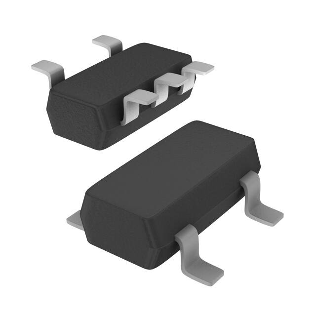
The LD6836CX4 and LD6836CX4/C devices are in a 0.4 mm pitch Wafer-Level
Chip-Scale Package (WLCSP) making them ideal for use in portable applications
requiring component miniaturization. The LD6836TD devices are in a small SOT753
Surface-Mounted Device (SMD) plastic package. All devices are manufactured in
monolithic silicon technology.
1.2 Features and benefits
300 mA output current rating
Input voltage range 2.3 V to 5.5 V
Fixed output voltage between 1.2 V and 3.6 V
Dropout voltage 90 mV at 300 mA output rating
Low quiescent current in shutdown mode (typical 0.1 A)
30 V RMS output noise voltage (typical value) at 10 Hz to 100 kHz
Turn-on time 150 s
55 dB Power Supply Rejection Ratio (PSRR) at 1 kHz
Over-temperature protection
Output current limiter
LD6836x/xxH: high-ohmic (3-state) output state when disabled
LD6836x/xxP: low-ohmic output state when disabled (auto discharge function)
Integrated ElectroStatic Discharge (ESD) protection up to 10 kV Human Body
Model (HBM)
WLCSP with 0.4 mm pitch and package size of 0.76 mm 0.76 mm 0.47 mm
Small SOT753 SMD plastic package (SOT23-5 compatible)
Pb-free, Restriction of Hazardous Substances (RoHS) compliant and free of halogen
and antimony (dark green compliant)
�LD6836 series
NXP Semiconductors
Ultra low dropout regulators, low noise, 300 mA
1.3 Applications
Analog and digital interfaces requiring lower than standard supply voltages in mobile
appliances such as smartphones, mobile phone handsets and cordless telephones. Other
typical applications are digital still cameras, mobile internet devices, personal navigation
devices and portable media players.
2. Pinning information
2.1 Pinning
bump A1
index area
1
2
A
5
4
B
001aao107
1
Fig 1.
2
transparent top view,
solder balls facing down
3
Pin configuration for SOT753
Fig 2.
Pin configuration for WLCSP4
2.2 Pin description
Table 1.
Symbol
Pin
Description
IN
1
regulator input voltage
GND
2
supply ground
EN
3
device enable input; active HIGH
n.c.
4
not connected
OUT
5
regulator output voltage
Table 2.
LD6836_SER
Product data sheet
Pin description for SOT753
Pin description for WLCSP4
Symbol
Pin
Description
GND
A1
supply ground
EN
A2
device enable input; active HIGH
OUT
B1
regulator output voltage
IN
B2
regulator input voltage
All information provided in this document is subject to legal disclaimers.
Rev. 2 — 5 October 2012
© NXP B.V. 2012. All rights reserved.
2 of 28
�LD6836 series
NXP Semiconductors
Ultra low dropout regulators, low noise, 300 mA
3. Ordering information
Table 3.
Ordering information
Type number
Package
Name
Description
LD6836CX4
WLCSP4
wafer-level chip-scale package; 4 bumps (2 2)
LD6836CX4/C
WLCSP4
wafer-level chip-scale package with backside
coating; 4 bumps (2 2) [1]
-
LD6836TD
-
plastic surface-mounted package; 5 leads
SOT753
[1]
Version
[1]
-
Size 0.76 mm 0.76 mm.
3.1 Ordering options
Further information on output voltage is available on request; see Section 18 “Contact
information”.
Table 4.
Type number
Nominal output
voltage
Type number
Nominal output
voltage
LD6836CX4/12H
1.2 V
LD6836CX4/25H
2.5 V
LD6836CX4/13H
1.3 V
LD6836CX4/27H
2.7 V
LD6836CX4/14H
1.4 V
LD6836CX4/28H
2.8 V
LD6836CX4/16H
1.6 V
LD6836CX4/29H
2.9 V
LD6836CX4/18H
1.8 V
LD6836CX4/30H
3.0 V
LD6836CX4/20H
2.0 V
LD6836CX4/33H
3.3 V
LD6836CX4/22H
2.2 V
LD6836CX4/36H
3.6 V
LD6836CX4/23H
2.3 V
-
-
Table 5.
LD6836_SER
Product data sheet
Type number extension of high-ohmic output in WLCSP4
Type number extension of pull-down output in WLCSP4
Type number
Nominal output
voltage
Type number
Nominal output
voltage
LD6836CX4/12P
1.2 V
LD6836CX4/23P
2.3 V
LD6836CX4/13P
1.3 V
LD6836CX4/25P
2.5 V
LD6836CX4/14P
1.4 V
LD6836CX4/27P
2.7 V
LD6836CX4/16P
1.6 V
LD6836CX4/28P
2.8 V
LD6836CX4/18P
1.8 V
LD6836CX4/29P
2.9 V
LD6836CX4/20P
2.0 V
LD6836CX4/30P
3.0 V
LD6836CX4/21P
2.1 V
LD6836CX4/33P
3.3 V
LD6836CX4/22P
2.2 V
LD6836CX4/36P
3.6 V
All information provided in this document is subject to legal disclaimers.
Rev. 2 — 5 October 2012
© NXP B.V. 2012. All rights reserved.
3 of 28
�LD6836 series
NXP Semiconductors
Ultra low dropout regulators, low noise, 300 mA
Table 6.
Type number
Nominal output
voltage
Type number
Nominal output
voltage
LD6836CX4/C12P
1.2 V
LD6836CX4/C23P
2.3 V
LD6836CX4/C13P
1.3 V
LD6836CX4/C25P
2.5 V
LD6836CX4/C14P
1.4 V
LD6836CX4/C27P
2.7 V
LD6836CX4/C16P
1.6 V
LD6836CX4/C28P
2.8 V
LD6836CX4/C18P
1.8 V
LD6836CX4/C29P
2.9 V
LD6836CX4/C20P
2.0 V
LD6836CX4/C30P
3.0 V
LD6836CX4/C21P
2.1 V
LD6836CX4/C33P
3.3 V
LD6836CX4/C22P
2.2 V
LD6836CX4/C36P
3.6 V
Table 7.
Product data sheet
Type number extension of high-ohmic output in SOT753
Type number
Nominal output
voltage
Type number
Nominal output
voltage
LD6836TD/12H
1.2 V
LD6836TD/23H
2.3 V
LD6836TD/13H
1.3 V
LD6836TD/27H
2.7 V
LD6836TD/14H
1.4 V
LD6836TD/28H
2.8 V
LD6836TD/16H
1.6 V
LD6836TD/29H
2.9 V
LD6836TD/18H
1.8 V
LD6836TD/30H
3.0 V
LD6836TD/20H
2.0 V
LD6836TD/33H
3.3 V
LD6836TD/22H
2.2 V
LD6836TD/36H
3.6 V
Table 8.
LD6836_SER
Type number extension of pull-down output in WLCSP4 with backside coating
Type number extension of pull-down output in SOT753
Type number
Nominal output
voltage
Type number
Nominal output
voltage
LD6836TD/12P
1.2 V
LD6836TD/23P
2.3 V
LD6836TD/13P
1.3 V
LD6836TD/25P
2.5 V
LD6836TD/14P
1.4 V
LD6836TD/27P
2.7 V
LD6836TD/16P
1.6 V
LD6836TD/28P
2.8 V
LD6836TD/18P
1.8 V
LD6836TD/29P
2.9 V
LD6836TD/20P
2.0 V
LD6836TD/30P
3.0 V
LD6836TD/21P
2.1 V
LD6836TD/33P
3.3 V
LD6836TD/22P
2.2 V
LD6836TD/36P
3.6 V
All information provided in this document is subject to legal disclaimers.
Rev. 2 — 5 October 2012
© NXP B.V. 2012. All rights reserved.
4 of 28
�LD6836 series
NXP Semiconductors
Ultra low dropout regulators, low noise, 300 mA
4. Block diagram
VIN
VOUT
R1
VEN
Vreference
GENERATOR
THERMAL
PROTECTION
R2
OVERCURRENT
PROTECTION
GND
001aan756
Fig 3.
Block diagram of LD6836x/xxH
VIN
VOUT
R1
VEN
Vreference
GENERATOR
THERMAL
PROTECTION
R2
OVER CURRENT
PROTECTION
GND
Fig 4.
LD6836_SER
Product data sheet
001aan299
Block diagram of LD6836x/xxP (auto discharge function)
All information provided in this document is subject to legal disclaimers.
Rev. 2 — 5 October 2012
© NXP B.V. 2012. All rights reserved.
5 of 28
�LD6836 series
NXP Semiconductors
Ultra low dropout regulators, low noise, 300 mA
5. Limiting values
Table 9.
Limiting values
In accordance with the Absolute Maximum Rating System (IEC 60134). Voltages are referenced to GND (ground = 0 V).
Symbol
Parameter
Conditions
VIN
voltage on pin IN
4 ms transient
total power dissipation
Ptot
Min
Max
Unit
0.5
+6.0
V
LD6836CX4, LD6836CX4/C
[1]
-
770
mW
LD6836TD
[1]
-
800
mW
Tstg
storage temperature
55
+150
C
Tj
junction temperature
40
+125
C
Tamb
ambient temperature
VESD
electrostatic discharge voltage
40
+85
C
human body model level 6
[2]
-
10
kV
machine model class 3
[3]
-
400
V
[1]
The (absolute) maximum power dissipation depends on the junction temperature Tj. Higher power dissipation is allowed with lower
ambient temperatures. The conditions to determine the specified values are Tamb = 25 C and the use of a two layer Printed-Circuit
Board (PCB).
[2]
According to IEC 61340-3-1.
[3]
According to JESD22-A115C.
6. Recommended operating conditions
Table 10. Operating conditions
Voltages are referenced to GND (ground = 0 V).
Symbol
Parameter
Tamb
Tj
Conditions
Min
Typ
Max
Unit
ambient temperature
40
-
+85
C
junction temperature
-
-
+125
C
voltage on pin IN
2.3
-
5.5
V
voltage on pin EN
0
-
VIN
V
0.7
1.0
-
F
Pin IN
VIN
Pin EN
VEN
Pin OUT
CL(ext)
[1]
[1]
external load capacitance
See Section 10.1 “Capacitor values”.
LD6836_SER
Product data sheet
All information provided in this document is subject to legal disclaimers.
Rev. 2 — 5 October 2012
© NXP B.V. 2012. All rights reserved.
6 of 28
�LD6836 series
NXP Semiconductors
Ultra low dropout regulators, low noise, 300 mA
7. Thermal characteristics
Table 11.
Symbol
Rth(j-a)
Thermal characteristics
Parameter
Conditions
thermal resistance from junction to ambient LD6836CX4, LD6836CX4/C
LD6836TD
Typ
Unit
[1][2]
130
K/W
[1][2]
125
K/W
[1]
The overall Rth(j-a) can vary depending on the board layout. To minimize the effective Rth(j-a), all pins must have a solid connection to
larger Cu layer areas for example to the power and ground layer. In multi-layer PCB applications, the second layer is used to create a
large heat spreader area directly below the LDO. If this layer is either ground or power, it is connected with several vias to the top layer
connecting to the device ground or supply. Avoid the use of solder-stop varnish under the chip.
[2]
Use the measurement data given for a rough estimation of the Rth(j-a) in your application. The actual Rth(j-a) value can vary in applications
using different layer stacks and layouts.
8. Characteristics
Table 12. Electrical characteristics
At recommended input voltages and Tamb = 40 C to +85 C; voltages are referenced to GND (ground = 0 V);
unless otherwise specified.
Symbol
Parameter
Conditions
Min
Typ
Max
Unit
dropout voltage
IOUT = 300 mA; VIN < VO(nom)
LD6836CX4, LD6836CX4/C
-
90
160
mV
LD6836TD
-
100
200
mV
Tamb = +25 C
3
0.5
+3
%
30 C Tamb +85 C
4
-
+4
%
Output voltage
Vdo
VO
output voltage variation
[1]
VOUT < 1.8 V; IOUT = 1 mA
VOUT 1.8 V; IOUT = 1 mA
Tamb = +25 C
2
0.5
+2
%
30 C Tamb +85 C
3
-
+3
%
0.1
-
+0.1
%/V
-
0.0025 0.01
%/mA
-
-
300
mA
350
-
-
mA
350
-
-
mA
-
600
-
mA
Line regulation error
VO/(VOxVI)
relative output voltage
variation with input voltage
VIN = (VO(nom) + 0.2 V) to 5.5 V
[1]
Load regulation error
VO/(VOxIO)
relative output voltage
variation with output current
1 mA IOUT 300 mA
Output current
IOUT
IOM
current on pin OUT
peak output current
VIN = (VO(nom) + 0.2 V) to 5.5 V
VO(nom) > 1.8V;
[1]
VOUT = 0.95 VO(nom)
VO(nom) < 1.8 V;
VOUT = 0.9 VO(nom)
Isc
short-circuit current
LD6836_SER
Product data sheet
pin OUT
All information provided in this document is subject to legal disclaimers.
Rev. 2 — 5 October 2012
© NXP B.V. 2012. All rights reserved.
7 of 28
�LD6836 series
NXP Semiconductors
Ultra low dropout regulators, low noise, 300 mA
Table 12. Electrical characteristics …continued
At recommended input voltages and Tamb = 40 C to +85 C; voltages are referenced to GND (ground = 0 V);
unless otherwise specified.
Symbol
Parameter
Conditions
Min
Typ
Max
Unit
Regulator quiescent current
quiescent current
Iq
VEN = 1.4 V; IOUT = 0 mA
-
70
100
A
VEN = 1.4 V; 1 mA IOUT 300 mA
-
155
250
A
VEN 0.4 V
-
0.1
1
A
-
55
-
dB
Ripple rejection and output noise
[1]
PSRR
power supply rejection ratio
VIN = VO(nom) + 1.0 V; IOUT = 30 mA;
fripple = 1 kHz
Vn(o)(RMS)
RMS output noise voltage
fripple = 10 Hz to 100 kHz;
CL(ext) = 1 F
-
30
-
V
0
-
0.4
V
1.1
-
5.5
V
-
150
-
s
-
300
-
s
-
100
-
Enable input and timing
VIL
LOW-level input voltage
pin EN
VIH
HIGH-level input voltage
pin EN
regulator start-up time
VIN = 5.5 V; VOUT = 0.95 VO(nom);
IOUT = 300 mA; CL(ext) = 1 F
tstartup(reg)
[1]
LD6836x/xxP; auto discharge function
tsd(reg)
regulator shutdown time
Rpd
pull-down resistance
VIN = 5.5 V; VOUT = 0.05 VO(nom);
CL(ext) = 1 F
Over-temperature protection
Tsd
shutdown temperature
-
160
-
C
Tsd(hys)
shutdown temperature
hysteresis
-
20
-
K
[1]
VO(nom) = nominal output voltage (device specific).
LD6836_SER
Product data sheet
All information provided in this document is subject to legal disclaimers.
Rev. 2 — 5 October 2012
© NXP B.V. 2012. All rights reserved.
8 of 28
�LD6836 series
NXP Semiconductors
Ultra low dropout regulators, low noise, 300 mA
9. Dynamic behavior
9.1 Power Supply Rejection Ratio (PSRR)
PSRR stands for the capability of the regulator to suppress unwanted signals on the input
voltage like noise or ripples.
V out ripple
for all frequencies
PSRR dB = 20 log -------------------------V in ripple
3655
�G%�
����������
�
,287�
,287�
,287�
,287�
,287�
,287�
���
������P$
������P$
������P$
������P$
����P$
�����P$
3655
�G%�
DDD�������
�
,287�
,287�
,287�
,287�
,287�
,287�
���
������P$
������P$
������P$
������P$
����P$
�����P$
���
���
���
���
���
���
���
���
���
IUHTXHQF\��+]�
���
���
���
VIN = 4.6 V; VOUT = 3.6 V; CL(ext) = 1 F
Fig 5.
���
IUHTXHQF\��+]�
���
VIN = 3.5 V; VOUT = 2.5 V; CL(ext) = 1 F
PSRR for LD6836CX4/36H
Fig 6.
3655
�G%�
���
PSRR of LD6836TD/25H
DDD�������
�
,287�
,287�
,287�
,287�
,287�
,287�
���
������P$
�����P$
����P$
������P$
������P$
������P$
���
���
���
���
���
���
IUHTXHQF\��+]�
���
VIN = 2.2 V; VOUT = 1.2 V; CL(ext) = 1 F
Fig 7.
PSRR of LD6836CX4/12H
LD6836_SER
Product data sheet
All information provided in this document is subject to legal disclaimers.
Rev. 2 — 5 October 2012
© NXP B.V. 2012. All rights reserved.
9 of 28
�LD6836 series
NXP Semiconductors
Ultra low dropout regulators, low noise, 300 mA
9.2 Dropout
The dropout voltage is defined as the smallest input to output voltage difference at a
specified load current when the regulator operates within its linear region. This means that
the input voltage is below the nominal output voltage value and the pass transistor works
as a plain resistor.
A small dropout voltage guarantees lower power consumption and efficiency
maximization.
DDD�������
���
9GR
�P9�
��
Fig 8.
���
7DPE� �����&
7DPE� �����&
7DPE� ������&
��
��
��
��
��
��
�
�
��
���
DDD�������
���
9GR
�P9�
���
���
,287��P$�
�
���
Dropout voltage as a function of output
current for LD6836CX4/25x
Fig 9.
7DPE� �����&
7DPE� �����&
7DPE� �����&
�
��
���
���
���
,287��P$�
���
Dropout voltage as a function of output
current for LD6836TD/36x
9.3 Accuracy
The LD6836 series guarantees high accuracy of the nominal output voltage.
DDD�������
����
,287� ���P$
9287
�9�
,287� ����P$
����
,287� �����P$
,287� �����P$
����
,287� �����P$
����
����
���
���
���
9,1��9�
���
Fig 10. Working voltage tolerance for LD6836CX4/25x
LD6836_SER
Product data sheet
All information provided in this document is subject to legal disclaimers.
Rev. 2 — 5 October 2012
© NXP B.V. 2012. All rights reserved.
10 of 28
�LD6836 series
NXP Semiconductors
Ultra low dropout regulators, low noise, 300 mA
9.4 Quiescent current
Quiescent (or ground) current is the difference between input and output current of the
regulator.
DDD�������
���
,*1'
��
��
��
��
�
���
���
��
��
��
7DPE��&�
��
IOUT = 0 mA
Fig 11. Quiescent current for LD6836CX4/25H
9.5 Noise
Output noise voltage of an LDO circuit is given as noise density or RMS output noise
voltage over a defined frequency spectrum (10 Hz to 100 kHz). Permanent conditions are
a constant output current and a ripple-free input voltage. The output noise voltage is
generated by the LDO regulator.
DDD�������
����
QRLVH
�ȝ9�Y+]�
,287�
,287�
,287�
,287�
,287�
,287�
����
�����P$
�����P$
���P$
����P$
���P$
�����P$
����
����
����
����
��
���
���
���
IUHTXHQF\��+]�
���
Fig 12. Noise density for LD6836x/25x
LD6836_SER
Product data sheet
All information provided in this document is subject to legal disclaimers.
Rev. 2 — 5 October 2012
© NXP B.V. 2012. All rights reserved.
11 of 28
�LD6836 series
NXP Semiconductors
Ultra low dropout regulators, low noise, 300 mA
9.6 Line Regulation
Line regulation is the capability of the circuit to maintain the nominal output voltage while
varying the input voltage.
DDD�������
�
9,1
�9�
9287
�9�
9287�
DDD�������
�
���
9287
9,1
�9�
���
9287
�9�
�
�
���
���
�
�
9,1�
�
�
���
���
���
WLPH��PV�
9,1
�
���
���
�
IOUT = 300 mA
���
���
���
WLPH��PV�
���
���
IOUT = 300 mA
Fig 13. Line regulation for LD6836CX4/33P
Fig 14. Line regulation for LD6836CX4/25P
9.7 Load Regulation
Load regulation is the capability of the circuit to maintain the nominal output voltage while
varying the output current.
DDD�������
���
,287
�$�
���
9287
�9�
9287
DDD�������
���
,287
�$�
���
9287
�9�
9287
���
���
���
���
���
���
���
���
,287
,287
����
�
���
���
���
���
���
���
���
���
WLPH��PV�
VIN = 5.5 V
Product data sheet
�
���
���
���
WLPH��PV�
���
���
VIN = 5.5 V
Fig 15. Load regulation for LD6836CX4/33P
LD6836_SER
����
Fig 16. Load regulation for LD6836CX4/25P
All information provided in this document is subject to legal disclaimers.
Rev. 2 — 5 October 2012
© NXP B.V. 2012. All rights reserved.
12 of 28
�LD6836 series
NXP Semiconductors
Ultra low dropout regulators, low noise, 300 mA
9.8 Start-up and shutdown
Start-up time defines the time needed for the LDO to achieve 95 % of its typical output
voltage level after activation via the enable pin. Shutdown time defines the time needed
for the LDO to pull-down the output voltage to 10 % of its nominal output voltage after
deactivation via the enable pin.
DDD�������
���
9HQDEOH
�9�
9287
9(1
���
DDD�������
���
9HQDEOH
�9�
���
�
9287
�9�
9287
�9�
�
9(1
�
�
�
�
���
�
�
���
���
�
���
�
���
9287
�
���
�
�
����
�
�
����
���
WLPH��PV�
���
Fig 17. Start-up for LD6836x/33P
�
���
���
���
WLPH��PV�
�
���
Fig 18. Shutdown for LD6836x/25P
9.9 Enable threshold voltage
An active HIGH signal enables the LDO when the signal exceeds the minimum input
HIGH voltage threshold. The LDO is in Off state as long the signal is below the maximum
LOW threshold. The input voltage threshold is independent from the LDO input voltage.
DDD�������
���
9287
�9�
���
+,*+�WR�/2:
���
/2:�WR�+,*+
���
����
���
���
���
���
���
���
9(1��9�
���
Fig 19. Enable threshold voltage
LD6836_SER
Product data sheet
All information provided in this document is subject to legal disclaimers.
Rev. 2 — 5 October 2012
© NXP B.V. 2012. All rights reserved.
13 of 28
�LD6836 series
NXP Semiconductors
Ultra low dropout regulators, low noise, 300 mA
10. Application information
10.1 Capacitor values
The LD6836 series require external capacitors at the output to guarantee a stable
regulator behavior. Do not under-run the specified minimum Equivalent Series
Resistance (ESR). The absolute value of the total capacitance attached to the output pin
OUT influences the shutdown time (tsd(reg)) of the LD6836 series. Also an input capacitor
is recommended to keep the input voltage stable.
Table 13.
External load capacitor
Symbol
Parameter
Conditions
Ci(ext)
external input capacitance
[1]
CL(ext)
external load capacitance
[1]
ESR
equivalent series resistance
[1]
Min
Typ
Max
Unit
0.7
1.0
0.7
1.0
-
F
5
-
500
m
F
The minimum value of capacitance for stability and correct operation is 0.7 F. The specified capacitor
tolerance is 30 % or better over the temperature and operating conditions range. The recommended
capacitor type is X7R to meet the full device temperature specification of 40 C to +125 C.
IN
IN
OUT
EN
GND
1μF
OUT
1μF
001aan647
Fig 20. Application diagram
LD6836_SER
Product data sheet
All information provided in this document is subject to legal disclaimers.
Rev. 2 — 5 October 2012
© NXP B.V. 2012. All rights reserved.
14 of 28
�LD6836 series
NXP Semiconductors
Ultra low dropout regulators, low noise, 300 mA
11. Test information
11.1 Quality information
This product has been qualified in accordance with NX1-00023 NXP Semiconductors
Quality and Reliability Specification and is suitable for use in consumer applications.
12. Marking
12.1 WLCSP4
WLCSP dies are laser marked with the following information (see Table 14 to 16 and
Figure 21):
1. Shaded area: marking of pin A1
2. The character N gives the version code and describes the output mode of the LDO. If
the code is legible, the LDO has an integrated pull down transistor (“P“ version). If the
character N is rotated counterclockwise by 90°, the LDO is a “H“ version.
3. “YYY” symbolizes a placeholder for some characters of the lot ID
7UDQVSDUHQW�WRS�YLHZ
DDD�������
Fig 21. Marking WLCSP4
Table 14.
LD6836_SER
Product data sheet
Marking code of high-ohmic output
Type number
Nominal output voltage
Marking code
LD6836CX4/12H
1.2 V
A
LD6836CX4/27H
2.7 V
P
All information provided in this document is subject to legal disclaimers.
Rev. 2 — 5 October 2012
© NXP B.V. 2012. All rights reserved.
15 of 28
�LD6836 series
NXP Semiconductors
Ultra low dropout regulators, low noise, 300 mA
Table 15.
Marking of pull-down output
Type number
Nominal
Marking
output voltage code
Type number
Nominal
Marking
output voltage code
LD6836CX4/12P 1.2 V
A
LD6836CX4/23P 2.3 V
L
LD6836CX4/13P 1.3 V
B
LD6836CX4/25P 2.5 V
N
LD6836CX4/14P 1.4 V
C
LD6836CX4/27P 2.7 V
P
LD6836CX4/16P 1.6 V
E
LD6836CX4/28P 2.8 V
Q
LD6836CX4/18P 1.8 V
G
LD6836CX4/29P 2.9 V
R
LD6836CX4/20P 2.0 V
I
LD6836CX4/30P 3.0 V
S
LD6836CX4/21P 2.1 V
J
LD6836CX4/33P 3.3 V
V
LD6836CX4/22P 2.2 V
K
LD6836CX4/36P 3.6 V
Y
Table 16.
Marking code of pull-down output with backside coating
Type number
Nominal
Marking
output voltage code
Type number
Nominal
Marking
output voltage code
LD6836CX4/C12P 1.2 V
A
LD6836CX4/C23P 2.3 V
L
LD6836CX4/C13P 1.3 V
B
LD6836CX4/C25P 2.5 V
N
LD6836CX4/C14P 1.4 V
C
LD6836CX4/C27P 2.7 V
P
LD6836CX4/C16P 1.6 V
E
LD6836CX4/C28P 2.8 V
Q
LD6836CX4/C18P 1.8 V
G
LD6836CX4/C29P 2.9 V
R
LD6836CX4/C20P 2.0 V
I
LD6836CX4/C30P 3.0 V
S
LD6836CX4/C21P 2.1 V
J
LD6836CX4/C33P 3.3 V
V
LD6836CX4/C22P 2.2 V
K
LD6836CX4/C36P 3.6 V
Y
12.2 SOT753
�
;