-6
LD6915 series
DF
N1
212
Dual low-dropout regulators, low noise, 150 mA
Rev. 1 — 8 July 2013
Objective data sheet
1. Product profile
1.1 General description
The LD6915 series consists of small-size dual Low DropOut regulators (LDO). Each
device delivers two times 150 mA with a typical voltage drop of 120 mV at 150 mA for
each LDO. The system offers two individual fixed nominal output voltages (VO(nom)) from
1.2 V to 3.6 V with high Power Supply Rejection Ratio (PSRR) of 80 dB.
The LDO has an integrated Soft start to control the inrush current during start-up. The
output mode, when disabled, can be high-ohmic 3-state or auto discharge. Optionally a
delayed output circuit is available for the second output. The devices are available in
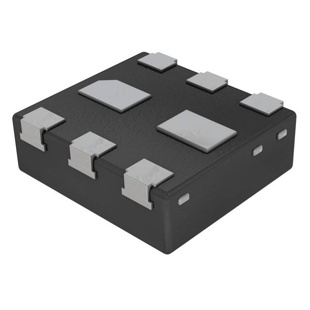
DFN1212-6 (SOT1229) package with a maximum height of 0.4 mm.
1.2 Features and benefits
Extremely low standby current in shutdown mode ( 0.1 A)
Low quiescent current
Fast turn-on time
Safety features (temperature watchdog, current limiter and foldback circuit)
Delayed output circuit for second LDO (optional)
High PSRR
Auto discharge or high-ohmic mode for output when disabled
DFN1212-6 (SOT1229) with 0.4 mm pitch and package size of 1.2 1.2 0.4 mm
Pb-free, Restriction of Hazardous Substances (RoHS) compliant, free of halogen and
antimony (Dark Green compliant)
1.3 Applications
Smartphones
Mobile handsets
Digital still cameras
Tablet PCs
Mobile internet devices
Portable media players
1.4 Quick reference data
IO = 150 mA for each LDO
PSRR = 80 dB at 1 kHz
RMS noise Vn(o)RMS = 60 V
at 10 Hz to 100 kHz
tstartup(reg) = 150 s
VI = 1.75 V to 5.5 V
VO = 1.2 V to 3.6 V (fixed value)
Dropout voltage Vdo = 120 mV
at IO = 150 mA for each LDO
Quiescent current Iq = 2 35 A at
IO = 0 mA
�LD6915 series
NXP Semiconductors
Dual low-dropout regulators, low noise, 150 mA
2. Pinning information
2.1 Pinning
1
6
2
5
3
4
Transparent top view
Fig 1.
Pin configuration for DFN1212-6 (SOT1229)
2.2 Pin description
Table 1.
Symbol
Pin
Description
OUT1
1
regulator 1 output voltage
OUT2
2
regulator 2 output voltage
GND
3
supply ground
EN2
4
regulator 2 enable input
IN
5
supply voltage input
EN1
6
regulator 1 enable input
i.c.
TAB
internal connected [1]
[1]
LD6915_SER
Objective data sheet
Pin description for DFN1212-6 (SOT1229)
The TAB is GND level (it is placed on the reverse side of the IC).
It is recommended to connect the TAB to GND. Leaving it unconnected is also allowed but it may result in
lower thermal performance.
All information provided in this document is subject to legal disclaimers.
Rev. 1 — 8 July 2013
© NXP B.V. 2013. All rights reserved.
2 of 25
�LD6915 series
NXP Semiconductors
Dual low-dropout regulators, low noise, 150 mA
3. Ordering information
Table 2.
Ordering information
Type number
Package
Name
LD6915LX
Description
Version
DFN1212-6 plastic extremely thin small outline package; no leads;
6 terminals; body 1.2 1.2 0.4 mm
SOT1229
3.1 Ordering options
Further output voltage versions are available on request; see Section 19 “Contact
information”
Table 3.
Type number and nominal output voltage of high-ohmic output
Type number
Nominal output voltage VO(nom)
OUT1
OUT2
LD6915LX/3028H
3.0 V
2.8 V
LD6915LX/3328H
3.3 V
2.8 V
Table 4.
Type number and nominal output voltage of auto discharge
Type number
Nominal output voltage VO(nom)
OUT1
OUT2
LD6915LX/1815P
1.8 V
1.5 V
LD6915LX/1828P
1.8 V
2.8 V
LD6915LX/2818P
2.8 V
1.8 V
LD6915LX/3018P
3.0 V
1.8 V
LD6915LX/3028P
3.0 V
2.8 V
LD6915LX/3318P
3.3 V
1.8 V
LD6915LX/3328P
3.3 V
2.8 V
LD6915LX/3333P
3.3 V
3.3 V
LD6915LX/3612P
3.6 V
1.2 V
Table 5.
Type number and nominal output voltage of high-ohmic output with delay circuit
Type number
Nominal output voltage VO(nom)
LD6915LX/3328HD
Table 6.
3.3 V
2.8 V
Nominal output voltage VO(nom)
LD6915LX/2818PD
Objective data sheet
OUT2
Type number and nominal output voltage of auto discharge with delay circuit
Type number
LD6915_SER
OUT1
OUT1
OUT2
2.8 V
1.8 V
All information provided in this document is subject to legal disclaimers.
Rev. 1 — 8 July 2013
© NXP B.V. 2013. All rights reserved.
3 of 25
�LD6915 series
NXP Semiconductors
Dual low-dropout regulators, low noise, 150 mA
4. Block diagram
,1
287�
62)7�67$57
(1�
(1�
9UHI
*(1(5$725
7+(50$/
3527(&7,21
'(/$
很抱歉,暂时无法提供与“LD6915LX/3018PH”相匹配的价格&库存,您可以联系我们找货
免费人工找货