LD6938 series
Dual low-dropout regulators, low noise, 300 mA
Rev. 1 — 11 July 2013
Objective data sheet
1. Product profile
1.1 General description
The LD6938 series consists of small-size dual Low DropOut regulators (LDO). Each
device delivers two times 300 mA with a typical voltage drop of 240 mV at full output load.
The devices offer two separate fixed nominal output voltages (VO(nom)) in the range of
1.2 V to 3.3 V.
The LDO has an integrated Soft start to control the inrush current during start-up. The
output mode, when disabled, can be high-ohmic 3-state or auto discharge. Optionally a
delayed start-up circuit is available for the second output. The devices are available in a
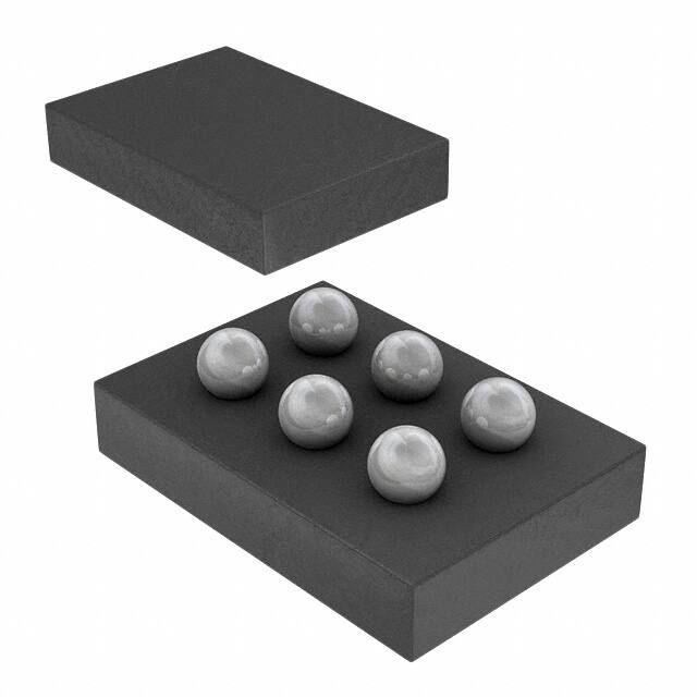
6-bump Wafer-Level Chip-Scale Package (WLCSP) with a height of 0.47 mm.
1.2 Features and benefits
High Power Supply Rejection Ratio (PSRR)
Low output noise
Low quiescent current
Extremely low standby current ( 0.1 A)
Soft start circuit to limit inrush current
Output current limiter with foldback circuit
Overtemperature protection
Delayed output circuit for second LDO (optional)
Auto discharge or high-ohmic mode for output when disabled
WLCSP6 with 0.4 mm pitch and package size of 1.2 mm 0.8 mm 0.47 mm
1.3 Applications
Smartphones
Mobile handsets
Digital still cameras
Tablet PCs
Mobile internet devices
Portable media players
1.4 Quick reference data
IO = 300 mA for each LDO
PSRR = 80 dB at 1 kHz
RMS noise Vn(o)RMS = 70 V
at 10 Hz to 100 kHz
tstartup(reg) 200 s
VI = 1.7 V to 5.5 V
VO = 1.2 V to 3.3 V (fixed value)
Drop voltage Vdo = 240 mV
at IO = 300 mA
Quiescent current Iq = 30 A for each
LDO at IO = 0 mA
�LD6938 series
NXP Semiconductors
Dual low-dropout regulators, low noise, 300 mA
2. Pinning information
2.1 Pinning
EDOO�$�
LQGH[�DUHD
/'����&;�
(1�
$�
$�
287�
*1'
%�
%�
,1
(1�
&�
&�
287�
DDD�������
WUDQVSDUHQW�WRS�YLHZ�
VROGHU�EDOOV�IDFLQJ�GRZQ
Fig 1.
Pin configuration for WLCSP6
2.2 Pin description
Table 1.
LD6938_SER
Objective data sheet
Pin description for WLCSP6
Symbol
Pin
Description
EN1
A1
regulator 1 enable input
OUT1
A2
regulator 1 output voltage
GND
B1
supply ground
IN
B2
supply voltage input
EN2
C1
regulator 2 enable input
OUT2
C2
regulator 2 output voltage
All information provided in this document is subject to legal disclaimers.
Rev. 1 — 11 July 2013
© NXP B.V. 2013. All rights reserved.
2 of 15
�LD6938 series
NXP Semiconductors
Dual low-dropout regulators, low noise, 300 mA
3. Ordering information
Table 2.
Ordering information
Type number
Package
Name
LD6938CX6
Description
Version
WLCSP6 wafer level chip-size package; 6 bumps (2 3)
-
3.1 Ordering options
Further output voltage versions and optional delay circuit for the second LDO are
available on request; see Section 15 “Contact information”.
Table 3.
Type number
Nominal output voltage VO(nom)
OUT1
OUT2
LD6938CX6/1818H
1.8 V
1.8 V
Table 4.
LD6938_SER
Objective data sheet
Type number extension of high ohmic output
Type number extension for auto discharge
Type number
Nominal output voltage VO(nom)
OUT1
OUT2
LD6938CX6/1215PL
1.2 V
1.5 V
LD6938CX6/1218PL
1.2 V
1.8 V
LD6938CX6/18125PL
1.8 V
1.25 V
LD6938CX6/1818PL
1.8 V
1.8 V
LD6938CX6/1833PL
1.8 V
3.3 V
LD6938CX6/285285PL
2.85 V
2.85 V
LD6938CX6/3018PL
3.0 V
1.8 V
LD6938CX6/3030PL
3.0 V
3.0 V
LD6938CX6/33285PL
3.3 V
2.85 V
LD6938CX6/3333PL
3.3 V
3.3 V
All information provided in this document is subject to legal disclaimers.
Rev. 1 — 11 July 2013
© NXP B.V. 2013. All rights reserved.
3 of 15
�LD6938 series
NXP Semiconductors
Dual low-dropout regulators, low noise, 300 mA
4. Block diagram
,1
287�
62)7�67$57
(1�
(1�
9UHI
*(1(5$725
7+(50$/
3527(&7,21
'(/$
很抱歉,暂时无法提供与“LD6938CX6/3030PLJ”相匹配的价格&库存,您可以联系我们找货
免费人工找货