Freescale Semiconductor
Data Sheet: Advance Information
Document Number: MC13850
Rev. 1, 12/2010
MC13850
Package Information
Plastic Package: MLPD-8
2.0 x 2.0 x 0.6 mm
Case: 2128-01
MC13850
Low Noise Amplifier with Bypass
Switch
1
Introduction
The MC13850 is a cost-effective, high IP3 LNA with low
noise figure. This is the leadless package version of the
MBC13720 device. As with the MBC13720, this device
is designed for general purpose RF applications, yet has
excellent high frequency gain and noise figure. An
integrated bypass switch is included to preserve high
input intercept performance. The input and output match
are external to allow maximum design flexibility. The
LNA has two selectable IP3 modes, a bypass mode and a
standby mode. The MC13850 is fabricated with an
advanced RF BiCMOS process using the SiGe:C module
and is packaged in the MLPD-8 leadless package.
1.1
•
•
•
Ordering Information
Device
Device Marking
Package
MC13850EP
850
MLPD-8
Contents:
1
2
3
4
5
6
7
8
Introduction . . . . . . . . . . . . . . . . . . . . . . . . . . . . .1
Electrical Specifications . . . . . . . . . . . . . . . . . . .3
Scattering and Noise Parameters . . . . . . . . . . . .8
Application Information . . . . . . . . . . . . . . . . . . .34
Printed Circuit Board and Bill of Materials . . .46
Packaging . . . . . . . . . . . . . . . . . . . . . . . . . . . . . .52
Product Documentation . . . . . . . . . . . . . . . . . . .53
Revision History . . . . . . . . . . . . . . . . . . . . . . . . .53
Features
RF input frequency: 400 MHz to 2500 MHz
Gain: 21 dB at 470 MHz, 14.5 dB at 1960 MHz
and 12 dB at 2.4 GHz in high IP3 mode
Input third order intercept point (IIP3): 10 dBm
at 1960 MHz, 13 dBm at 2.4 GHz, and -2.5 dBm
at 860 MHz in high IP3 mode
This document contains information on a new product. Specifications and information herein are subject to change without notice.
© Freescale Semiconductor, Inc., 2006–2010. All rights reserved.
�Introduction
•
•
•
•
•
•
•
•
•
•
•
•
•
Noise Figure (NF): 1.6 dB at 860 MHz, 1.4 dB at 1960 MHz, and 1.55 dB at 2400 MHz in low IP3
mode
Output 1 dB compression point (P1dB): 9 dBm at 470 MHz and 11.5 dBm at 1060 MHz in high
IP3 mode
Selectable IP3 mode allows for running at the desired IP3 performance for a receiver's linearity
requirements
Bypass mode has return losses comparable to active mode, for use in systems with filters and
duplexers
Bypass mode improves dynamic range in variable signal strength environments
Integrated logic-controlled standby mode with current drain < 1µA
Total supply current: 5 mA at 2.7 V in low IP3 mode and 10 mA in high IP3 mode. Bypass mode
21 dB, OIP3 of 10 dBm with return
losses better than -10 dB at 470 MHz and NF < 1.3 dB, S21 gain > 17 dB, OIP3 of 13 dBm at 860 MHz.
This is a broadband application with application to UHF. The performance can be further optimized for
narrowband applications such as RKE at the lower frequency, or wireless security at the higher frequency.
Typical performance that can be expected from this circuit at 2.7V is listed in Table 17.
Figure 14 shows the 470 MHz–860 MHz schematic with package pinouts and circuit components.
En able 1
Vcc
En ab le 2
8
7
6
5
R1
0402
330 ohm
Gain
Logic
C5
0402
.1 uF
Enable
Pin 1
Locator
on
Package
C4
0402
47 pF
L3
0402
4.3 nH
1
2
3
L2
0402
18 nH
4
NC
RF IN
Gnd
C1
0402
27 pF
L1
0402
47 nH
C2
0402
.1 uF
C3
0402
5 pF
R2
0402
51 ohm
.
RF
OUT
Figure 14. 470 MHz–860 MHz Application Schematic
Table 17. Typical 470 MHz–860 MHz Evaluation Board Performance
(Vcc = 2.7V, TA = 25°C)
Characteristic
Symbol
Min
Typ
Max
Unit
Low IP3
—
4.7
5.7
mA
High IP3
—
9.9
12.5
mA
Bypass
—
2
10
uA
Low IP3
20.5
21.6
—
High IP3
23.4
24.4
—
Bypass
-7.4
-6.9
—
470 MHz (refer to Figure 14)
Supply Current
RF Gain
Icc
G
dB
MC13850 Advance Information, Rev. 1
Freescale Semiconductor
35
�Application Information
Table 17. Typical 470 MHz–860 MHz Evaluation Board Performance (continued)
(Vcc = 2.7V, TA = 25°C)
Characteristic
Symbol
Min
Typ
Max
Low IP3
—
1.32
1.6
High IP3
—
1.33
1.6
Bypass
—
9.5
10
Low IP3
-12.5
-11.2
—
High IP3
-9.2
-8
—
Bypass
26.7
27.7
—
Low IP3
6
7
—
High IP3
8.6
9.6
—
Low IP3
—
-5.2
-4.1
High IP3
—
-10.6
-8.5
Bypass
—
-4.2
-3.2
Low IP3
20.5
21.5
—
High IP3
23.1
24.1
—
Bypass
-7.7
-6.7
—
Low IP3
—
-27.3
-20
High IP3
—
-30.6
-25
Bypass
—
-6.7
-6.2
Low IP3
—
-6.6
-5.6
High IP3
—
-10.2
-9.2
Bypass
—
-11.7
-10.7
Noise Figure
Unit
NF
dB
Input IP3
IIP3
dBm
Power Output at 1.0 dB
Gain Compression
Input Return Loss
P1dBoutput
dBm
S11
dB
Gain
S21
dB
Reverse Isolation
S12
dB
Output Return Loss
S22
dB
MC13850 Advance Information, Rev. 1
36
Freescale Semiconductor
�Application Information
Table 17. Typical 470 MHz–860 MHz Evaluation Board Performance (continued)
(Vcc = 2.7V, TA = 25°C)
Characteristic
Symbol
Min
Typ
Max
Low IP3
16.4
17.4
—
High IP3
18
19
—
Bypass
-6.7
-6.2
—
Low IP3
—
1.22
1.5
High IP3
—
1.32
1.6
Bypass
—
5.2
5.7
Unit
860 MHz (refer to Figure 14)
RF Gain
G
dB
Noise Figure
NF
dB
Input IP3
IIP3
dBm
Low IP3
-5.3
-4
—
High IP3
-2.3
-1.1
—
Bypass
23.7
24.7
—
Power Output at 1.0 dB
Gain Compression
P1dB
dBm
Low IP3
7.4
8.4
—
High IP3
8.1
9.2
—
Input Return Loss
S11
dB
Low IP3
—
-13.7
-11
High IP3
—
-21.3
-17
Bypass
—
-6
-5
Low IP3
17
18
—
High IP3
18.4
19.4
—
Bypass
-6.8
-5.8
—
Low IP3
—
-26.9
-25
High IP3
—
-29.2
-28.2
Bypass
—
-5.7
-5
Gain
S21
dB
Reverse Isolation
S12
dB
MC13850 Advance Information, Rev. 1
Freescale Semiconductor
37
�Application Information
Table 17. Typical 470 MHz–860 MHz Evaluation Board Performance (continued)
(Vcc = 2.7V, TA = 25°C)
Characteristic
Symbol
Min
Typ
Max
Low IP3
—
-5.3
-4.3
High IP3
—
-7.2
-6.2
Bypass
—
-8.2
-7.2
Output Return Loss
Unit
S22
dB
4.2
900 MHz Application
This application was designed to provide NF < 1.4 dB, S21 gain > 21 dB, OIP3 of 17 dBm with return
losses better than -10 dB at 900 MHz. Typical performance that can be expected from this circuit at 2.7V
is listed in Table 18.
Figure 15 shows the 900 MHz schematic with package pinouts and circuit components.
Enable2
Enable1
8
7
6
Vcc
5
R1
0402
330 ohm
Gain
L ogic
C5
0402
.1 uF
Enable
Pin 1
Locator
on
Package
C4
0402
47 pF
L3
0402
4.3 nH
1
2
3
L2
0402
8.2 nH
4
NC
RF IN
Gnd
L1
0402
22 nH
C2
0402
.1 uF
C1
0402
27 pF
.
RF
OUT
R2
0402
15 ohm
C3
0402
2.7
pF
Figure 15. 900 MHz Application Schematic
Table 18. Typical 900 MHz Evaluation Board Performance
(Vcc = 2.7V, Ta = 25°C)
Characteristic
Symbol
Min
Typ
Max
Unit
Low IP3
—
4.7
5.7
mA
High IP3
—
9.9
12.5
mA
900 MHz (refer to Figure 15)
Supply Current
Icc
MC13850 Advance Information, Rev. 1
38
Freescale Semiconductor
�Application Information
Table 18. Typical 900 MHz Evaluation Board Performance (continued)
(Vcc = 2.7V, Ta = 25°C)
Characteristic
Symbol
Min
Typ
Max
Unit
—
2
10
uA
Low IP3
20
21
—
High IP3
20.8
21.8
—
Bypass
-4.5
-3.7
—
Low IP3
—
1.38
1.6
High IP3
—
1.53
1.75
Bypass
—
3.85
4.6
Low IP3
-6.5
-4.1
—
High IP3
1.75
3.5
—
Bypass
27
27.6
—
Low IP3
10.9
11.9
—
High IP3
11.1
12.1
—
Low IP3
—
-10.7
-7
High IP3
—
-15.3
-12
Bypass
—
-9.5
-8
Low IP3
20.1
21.1
—
High IP3
20.8
21.8
—
Bypass
-4.5
-3.5
—
Low IP3
—
-23.9
-22.8
High IP3
—
-26.8
-25.7
Bypass
—
-3.5
-2.5
Low IP3
—
-10.7
-9.6
High IP3
—
-18.4
-15
Bypass
—
-18
-12.6
Bypass
RF Gain
G
dB
Noise Figure
NF
dB
Input IP3
IIP3
dBm
Power Output at 1.0 dB Gain Compression P1dBoutput
Input Return Loss
dBm
S11
dB
Gain
S21
dB
Reverse Isolation
S12
dB
Output Return Loss
S22
dB
MC13850 Advance Information, Rev. 1
Freescale Semiconductor
39
�Application Information
4.3
900 MHz High IP3 Application
This application was designed to demonstrate performance at 900 MHz using capacitive feedback from
the output to input to raise IP3. Typical performance that can be expected from this circuit at 2.75V is listed
in Table 19.
Figure 16 shows the High IP3 900 MHz schematic with package pinouts and circuit components. This
900 MHz application differs from the 900 MHz application in Section 4.2, “900 MHz Application in that
it uses output to input feedback capacitance to raise the IP3 performance.
Enable 1
8
Enable2
7
6
Vcc
5
R1
0402
330 ohm
Gain
Logic
C7
0402
.1 uF
Enable
Pin 1
Locator
on
Package
C8
0402
47 pF
C1
0402
100 pF
1
2
3
4
NC
RF IN
Gnd
C2
0402
.1 uF
L1
0402
9.1 nH
.
C3
0402
0.5 pF
L2
0402
5.6 nH
R2
0402
10 ohm
C5
0402
1pF
RF
OUT
C6
0402
5.1 pF
C4
0402
0.5 pF
Figure 16. 900 MHz High IP3 Application Schematic
Table 19. Typical 900 MHz High IP3 Evaluation Board Performance
(Vcc - 2.75V, TA = 25°C)
Characteristic
Symbol
Min
Typ
Max
Unit
Low IP3
—
4.7
5.7
mA
High IP3
—
9.9
12.5
mA
Bypass
—
2
10
uA
Low IP3
15.5
16.5
—
High IP3
16.1
17.1
—
Bypass
-5.2
-4.2
—
900 MHz (refer to Figure 16)
Supply Current
RF Gain
Icc
G
dB
MC13850 Advance Information, Rev. 1
40
Freescale Semiconductor
�Application Information
Table 19. Typical 900 MHz High IP3 Evaluation Board Performance (continued)
(Vcc - 2.75V, TA = 25°C)
Characteristic
Min
Typ
Max
Low IP3
—
1.43
1.65
High IP3
—
1.55
1.75
Bypass
—
4.6
5.8
Low IP3
-6
-2.9
—
High IP3
6
8
—
Bypass
26.2
27.7
—
Low IP3
8
12
—
High IP3
11.5
13.5
—
Low IP3
—
-12
-8
High IP3
—
-10
-8
Bypass
—
-9
-7
Low IP3
15.7
16.7
—
High IP3
16.2
17.2
—
Bypass
-4.7
-3.9
—
Low IP3
—
-19.3
-17.5
High IP3
—
-22.4
-21
Bypass
—
-3.9
-3.2
Low IP3
—
-11
-8.5
High IP3
—
-12.8
-10
Bypass
—
-31
-24
Noise Figure
Symbol
Unit
NF
dB
Input IP3
IIP3
dBm
Power Output at 1.0 dB Gain Compression P1dBoutput
Input Return Loss
dBm
S11
dB
Gain
S21
dB
Reverse Isolation
S12
dB
Output Return Loss
S22
dB
MC13850 Advance Information, Rev. 1
Freescale Semiconductor
41
�Application Information
4.4
1960 MHz Application
This application was designed to provide NF = 1.5 dB, S21 gain > 15 dB, OIP3 of 20 dBm with return
losses better than -10 dB at 1960 MHz. Typical performance that can be expected from this circuit at 2.7V
is listed in Table 20.
Figure 17 shows the 1960 MHz schematic with package pinouts and circuit components.
Enable2
Enable1
8
7
6
Vcc
5
R1
0402
330 ohm
Gain
Logic
Enable
Pin 1
Locator
on
Package
C4
0402
33 pF
C1
0402
27 pF
1
3
2
L2
0402
2.7 nH
4
NC
RF IN
Gnd
L1
0402
3.3 nH
L1
0402
33 nH
C5
0402
.1 uF
.
C3
0402
27 pF
R2
0402
5 ohm
RF
OUT
C2
0402
.1 uF
Figure 17. 1960 MHz Application Schematic
Table 20. Typical 1900 MHz Evaluation Board Performance
(Vcc = 2.7V, Ta = 25°C)
Characteristic
Symbol
Min
Typ
Max
Unit
Low IP3
—
4.7
5.7
mA
High IP3
—
9.9
12.5
mA
Bypass
—
2
10
uA
Low IP3
13.8
14.8
—
High IP3
13.9
14.9
—
Bypass
-4.8
-3.5
—
1960 MHz (refer to Figure 17)
Supply Current
RF Gain
Icc
G
dB
MC13850 Advance Information, Rev. 1
42
Freescale Semiconductor
�Application Information
Table 20. Typical 1900 MHz Evaluation Board Performance (continued)
(Vcc = 2.7V, Ta = 25°C)
Characteristic
Min
Typ
Max
Low IP3
—
1.5
1.8
High IP3
—
1.75
2
Bypass
—
3.2
4.4
Low IP3
3.5
6.5
—
High IP3
8
9.6
—
Bypass
22.6
23.6
—
Low IP3
1.5
3.2
—
High IP3
2.3
4
—
Low IP3
—
-12
-9.5
High IP3
—
-12.5
-10
Bypass
—
-11
-8
Low IP3
14
15
—
High IP3
14
15
—
Bypass
-4.8
-3.6
—
Low IP3
—
-21
-20
High IP3
—
-22.5
-21.5
Bypass
—
-3.7
-2.5
Low IP3
—
-13
-9
High IP3
—
-15
-11
Bypass
—
-8
-6
Noise Figure
Symbol
Unit
NF
dB
Input IP3
IIP3
dBm
Power Output at 1.0 dB Gain Compression P1dBoutput
Input Return Loss
dBm
S11
dB
Gain
S21
dB
Reverse Isolation
S12
dB
Output Return Loss
S22
dB
MC13850 Advance Information, Rev. 1
Freescale Semiconductor
43
�Application Information
4.5
2400 MHz Application
This application was designed to provide NF = 1.6 dB, S21 gain = 12 dB, OIP3 of 23 dBm at 2400 MHz.
Typical performance that can be expected from this circuit at 2.7V is listed in Table 21.
Figure 18 shows the 2400 MHz schematic with package pinouts and circuit components.
Ena ble1
8
En ab le2
7
6
Vcc
5
R1
0402
330 ohm
Gain
Lo g ic
C5
0402
.1 uF
Enable
Pin 1
L o cato r
on
Pa ckag e
C4
0402
33 pF
C1
0402
5 pF
1
2
3
L2
0402
3.3 nH
4
NC
R F IN
Gn d
L1
0402
3 nH
C3
0402
27 pF
R2
0402
5 ohm
.
RF
OUT
C2
0402
.1 uF
Figure 18. 2400 MHz Application Schematic
Table 21. Typical 2400 MHz Evaluation Board Performance
(Vcc = 2.7V, Ta = 25°C)
Characteristic
Symbol
Min
Typ
Max
Unit
Low IP3
—
4.7
5.7
mA
High IP3
—
9.9
12.5
mA
Bypass
—
2
10
uA
Low IP3
11.5
12.5
—
High IP3
12
13
—
Bypass
-4
-3
—
2400 MHz (refer to Figure 18)
Supply Current
RF Gain
Icc
G
dB
MC13850 Advance Information, Rev. 1
44
Freescale Semiconductor
�Application Information
Table 21. Typical 2400 MHz Evaluation Board Performance (continued)
(Vcc = 2.7V, Ta = 25°C)
Characteristic
Min
Typ
Max
Low IP3
—
1.6
1.95
High IP3
—
1.85
2.2
Bypass
—
3.2
4.3
Low IP3
7
10
—
High IP3
11
12.5
—
Bypass
26
27.2
—
Low IP3
-1
1
—
High IP3
0
2.2
—
Low IP3
—
-9
-7.5
High IP3
—
-9.5
-8
Bypass
—
-19.5
-12
Low IP3
11.6
12.6
—
High IP3
12
13
—
Bypass
-3.7
-3.2
—
Low IP3
—
-20
-19
High IP3
—
-20.6
-20
Bypass
—
-2.9
-2.4
Low IP3
—
-25
-15
High IP3
—
-27
-15
Bypass
—
-16
-10
Noise Figure
Symbol
Unit
NF
dB
Input IP3
IIP3
dBm
Power Output at 1.0 dB Gain Compression P1dBoutput
Input Return Loss
dBm
S11
dB
Gain
S21
dB
Reverse Isolation
S12
dB
Output Return Loss
S22
dB
MC13850 Advance Information, Rev. 1
Freescale Semiconductor
45
�Printed Circuit Board and Bill of Materials
5
Printed Circuit Board and Bill of Materials
Figure 19 is a drawing of the printed circuit board. Figure 21 through Figure 25 are drawings of the
evaluation boards used for each of the application frequency designs described in Section 4. These
drawings show the boards with the circuit matching components placed and identified.
Note: Dimensions are in inches and [mm].
Soldering Note: The center flag under the part needs to be soldered down to ground on the bo
Figure 19. Printed Circuit Board
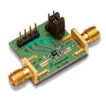
Figure 20. Typical Assembled Evaluation Board with SMA Connectors
MC13850 Advance Information, Rev. 1
46
Freescale Semiconductor
�Printed Circuit Board and Bill of Materials
Figure 21. 470–860 MHz Application Board
Figure 22. 900 MHz Application Board
MC13850 Advance Information, Rev. 1
Freescale Semiconductor
47
�Printed Circuit Board and Bill of Materials
Figure 23. 900 MHz High IP3 Application Board
Figure 24. 1960 MHz Application Board
MC13850 Advance Information, Rev. 1
48
Freescale Semiconductor
�Printed Circuit Board and Bill of Materials
Figure 25. 2400 MHz Application Board
The Bill of Materials for each of the application frequency circuit boards is listed in Table 22. The value,
case size, manufacturer and circuit function of each component are provided.
Table 22. Bill of Materials for the Application Circuit Boards
Component
Value
Case
Manufacturer
Comments
470–860 MHz (refer to Figure 21)
C1
27 pF
402
Murata
DC block, input match
C2
0.1 uF
402
Murata
Low freq. bypass
C3
5 pF
402
Murata
DC block, output match
C4
47 pF
402
Murata
860 MHz short
C5
0.1 uF
402
Murata
Low freq. bypass
L1
47 nH
402
Murata
Input match
L2
18 nH
402
Murata
Output match, bias decouple
L3
4.3 nH
402
Murata
Input match
R1
330 Ω
402
KOA
Logic circuit bias
R2
51 Ω
402
KOA
Lower gain, improve return losses
900 MHz (refer to Figure 22)
C1
27 pF
402
Murata
DC block, input match
C2
0.1 uF
402
Murata
DC block, input match
C3
2.7 pF
402
Murata
DC block, output match
C4
47 pF
402
Murata
900 MHz short
C5
0.1 uF
402
Murata
Low freq. bypass
L1
22 nH
402
Murata
Input match
MC13850 Advance Information, Rev. 1
Freescale Semiconductor
49
�Printed Circuit Board and Bill of Materials
Table 22. Bill of Materials for the Application Circuit Boards (continued)
Component
Value
Case
Manufacturer
Comments
L2
8.2 nH
402
Murata
Output match, bias decouple
L3
4.3 nH
402
Murata
Input match
R1
330 Ω
402
KOA
Logic circuit bias
R2
15 Ω
402
KOA
Lower gain, improve return losses
900 MHz High IP3 (refer to Figure 23)
C1
100 pF
402
Murata
DC block, input match
C2
0.1 uF
402
Murata
DC block, input match
C3
0.5 pF
402
Murata
IP3 improvement
C4
0.5 pF
402
Murata
IP3 improvement
C5
1.0 pF
402
Murata
Output match
C6
5.1 pF
402
Murata
Output match
C7
0.1 uF
402
Murata
Bypass
C8
47 pF
402
Murata
900 MHz short
L1
9.1 nH
402
Murata
Input match
L2
5.6 nH
402
Murata
Output match
R1
330 Ω
402
KOA
Logic circuit bias
R2
10 Ω
402
KOA
Lower gain, increase stability
1960 MHz (refer to Figure 24)
C1
27 pF
402
Murata
DC block, input match
C2
0.1 uF
402
Murata
DC block
C3
27 pF
402
Murata
DC block, output match
C4
33 pF
402
Murata
1960 MHz short
C5
0.1 uF
402
Murata
Low freq. bypass
L1
33 nH
402
Murata
Input match
L2
3.3 nH
402
Murata
Input match
L3
2.7 nH
402
Murata
Output match, bias decouple
R1
330 Ω
402
KOA
Logic circuit bias
R2
5Ω
402
KOA
Lower gain, increase stability
2400 MHz (refer to Figure 25)
C1
5 pF
402
Murata
DC block, input match
C2
0.1 uF
402
Murata
DC block
C3
27 pF
402
Murata
DC block, output match
MC13850 Advance Information, Rev. 1
50
Freescale Semiconductor
�Printed Circuit Board and Bill of Materials
Table 22. Bill of Materials for the Application Circuit Boards (continued)
Component
Value
Case
Manufacturer
Comments
C4
33 pF
402
Murata
1960 MHz short
C5
0.1 uF
402
Murata
Low freq. bypass
L1
3 nH
402
Murata
Input match
L2
3.3 nH
402
Murata
Input match
R1
330 Ω
402
KOA
Logic circuit bias
R2
5Ω
402
KOA
Lower gain, increase stability
MC13850 Advance Information, Rev. 1
Freescale Semiconductor
51
�Packaging
6
Packaging
Figure 26 and Figure 27 are the package drawings with dimensions for the MLPD-8, 2 × 2 × 0.6 mm,
package.
DETAIL G
(See Figure 27)
Figure 26. Outline Dimensions for MLPD-8
MC13850 Advance Information, Rev. 1
52
Freescale Semiconductor
�Product Documentation
Figure 27. Packaging Details
7
Product Documentation
This data sheet is labeled as a particular type: Product Preview, Advance Information, or Technical Data.
Definitions of these types are available at: http://www.freescale.com.
8
Revision History
Table 23 summarizes the revisions to this document since Rev. 0.
Table 23. Revision History
Revision
Description of Change
0
Initial Release
1
Technical Content Changes include:
• In Table 4, min and max values added.
• Added Table 5–Table 16, S parameters.
• Added Figure 2–Figure 9, constant gain and noise figure circles.
• Added Figure 10,Figure 11, minimum NF and associated gain.
• Added Figure 12, Figure 13, maximum stable gain and forward insertion gain.
• Section 4 application circuit performance parameters extensively revised.
• Section 5 printed circuit board and application board drawings added.
• Table 22 bill of materials for application revised.
• Section 6 package drawing changed to MLPD-8 package.
MC13850 Advance Information, Rev. 1
Freescale Semiconductor
53
�How to Reach Us:
Home Page:
www.freescale.com
Web Support:
http://www.freescale.com/support
USA/Europe or Locations Not Listed:
Freescale Semiconductor, Inc.
Technical Information Center, EL516
2100 East Elliot Road
Tempe, Arizona 85284
1-800-521-6274 or +1-480-768-2130
www.freescale.com/support
Europe, Middle East, and Africa:
Freescale Halbleiter Deutschland GmbH
Technical Information Center
Schatzbogen 7
81829 Muenchen, Germany
+44 1296 380 456 (English)
+46 8 52200080 (English)
+49 89 92103 559 (German)
+33 1 69 35 48 48 (French)
www.freescale.com/support
Japan:
Freescale Semiconductor Japan Ltd.
Headquarters
ARCO Tower 15F
1-8-1, Shimo-Meguro, Meguro-ku,
Tokyo 153-0064
Japan
0120 191014 or +81 3 5437 9125
support.japan@freescale.com
Asia/Pacific:
Freescale Semiconductor China Ltd.
Exchange Building 23F
No. 118 Jianguo Road
Chaoyang District
Beijing 100022
China
+86 10 5879 8000
support.asia@freescale.com
For Literature Requests Only:
Freescale Semiconductor Literature Distribution Center
1-800-441-2447 or +1-303-675-2140
Fax: +1-303-675-2150
LDCForFreescaleSemiconductor@hibbertgroup.com
Document Number: MC13850
Rev. 1
12/2010
Information in this document is provided solely to enable system and software
implementers to use Freescale Semiconductor products. There are no express or
implied copyright licenses granted hereunder to design or fabricate any integrated
circuits or integrated circuits based on the information in this document.
Freescale Semiconductor reserves the right to make changes without further notice to
any products herein. Freescale Semiconductor makes no warranty, representation or
guarantee regarding the suitability of its products for any particular purpose, nor does
Freescale Semiconductor assume any liability arising out of the application or use of any
product or circuit, and specifically disclaims any and all liability, including without
limitation consequential or incidental damages. “Typical” parameters that may be
provided in Freescale Semiconductor data sheets and/or specifications can and do vary
in different applications and actual performance may vary over time. All operating
parameters, including “Typicals”, must be validated for each customer application by
customer’s technical experts. Freescale Semiconductor does not convey any license
under its patent rights nor the rights of others. Freescale Semiconductor products are
not designed, intended, or authorized for use as components in systems intended for
surgical implant into the body, or other applications intended to support or sustain life,
or for any other application in which the failure of the Freescale Semiconductor product
could create a situation where personal injury or death may occur. Should Buyer
purchase or use Freescale Semiconductor products for any such unintended or
unauthorized application, Buyer shall indemnify and hold Freescale Semiconductor and
its officers, employees, subsidiaries, affiliates, and distributors harmless against all
claims, costs, damages, and expenses, and reasonable attorney fees arising out of,
directly or indirectly, any claim of personal injury or death associated with such
unintended or unauthorized use, even if such claim alleges that Freescale
Semiconductor was negligent regarding the design or manufacture of the part.
Freescale™ and the Freescale logo are trademarks of Freescale Semiconductor, Inc.
All other product or service names are the property of their respective owners.
© Freescale Semiconductor, Inc. 2006-2010. All rights reserved.
RoHS-compliant and/or Pb-free versions of Freescale products have the functionality
and electrical characteristics as their non-RoHS-compliant and/or non-Pb-free
counterparts. For further information, see http://www.freescale.com or contact your
Freescale sales representative.
For information on Freescale’s Environmental Products program, go to
http://www.freescale.com/epp.
�