Freescale Semiconductor
Data Sheet: Advance Information
Document Number: MC13851
Rev. 2.0, 12/2010
MC13851
Package Information
Plastic Package:
MLPD-8
2.0 × 2.0 × 0.6 mm
Case: 2128-01
MC13851
General Purpose Low Noise
Amplifier with Bypass Switch
1
Introduction
The MC13851 is a cost-effective, high IP3 LNA with low
noise figure. This is the smaller leadless package version
of the MC13821 device. The MC13851 includes an
integrated bypass switch to preserve high input intercept
performance in variable signal strength environments
and boosts dynamic range. On-chip bias circuitry offers
low system cost. The input and output match are external
to allow maximum design flexibility. An external resistor
is used to set device current which allows balancing
required linearity with low current consumption. Gain is
optimized for applications greater than 1000 MHz. The
MC13851 is fabricated with the advanced RF BiCMOS
process using the eSiGe:C module and is available in the
2 × 2 mm MLPD-8 leadless package, offering a small,
low height, easy-to-solder solution for applications with
tight printed circuit board placement requirements.
Ordering Information
Device
Device Marking
Package
MC13851EP
851
MLPD-8
Contents:
1
2
3
4
5
6
7
8
Introduction . . . . . . . . . . . . . . . . . . . . . . . . . . . . .1
Electrical Specifications . . . . . . . . . . . . . . . . . . .3
Application Information . . . . . . . . . . . . . . . . . . . .9
Printed Circuit and Bill of Materials . . . . . . . . .20
Scattering and Noise Parameters . . . . . . . . . . .22
Packaging . . . . . . . . . . . . . . . . . . . . . . . . . . . . . .32
Product Documentation . . . . . . . . . . . . . . . . . . .33
Revision History . . . . . . . . . . . . . . . . . . . . . . . . .33
This document contains information on a new product. Specifications and information herein are subject to change without notice.
© Freescale Semiconductor, Inc., 2006–2010. All rights reserved.
�Introduction
1.1
Features
The MC13851 is intended for applications from 1000 MHz to 2500 MHz and the MC13852 is for
applications less than 1000 MHz.
• Gain: 18.7 dB (typical) at 1960 MHz and 17.7 dB (typical) at 2140 MHz
• Output third order intercept point (OIP3): 16 dBm at 1960 MHz and 17 dBm (typical) dBm at
2140 MHz
• Noise Figure (NF): 1.37 dB (typical) at 1960 MHz and 1.46 dB at 2140 MHz
• Output 1 dB compression point (P1dB): 8 dBm (typical) at 1960 MHz and 8 dBm (typical) at
2140 MHz
• IP3 Boost Circuitry from Freescale
• Bypass mode has return losses comparable to active mode, for use in systems with filters and
duplexers
• Bypass mode improves dynamic range in variable signal strength environments
• Integrated logic-controlled standby mode with current drain < 1uA
• Total supply current variable from 2.5 mA–5 mA using an external bias resistor
• In a receiver system with 20% active mode and 80% bypass mode, the average current drain is < 0.6
mA
• On-chip bias sets the bias point
• Bias stabilized for device and temperature variations
• MLPD-8 leadless package with low parasitics
• 1575 MHz, 1960 MHz, 2140 MHz and 2500 MHz application circuit evaluation boards with
characterization data are available
• Available in tape and reel packaging
1.2
Applications
Ideal for use in any RF product that operates between 1000 MHz and 2.5 GHz, and may be applied in:
• Buffer amplifiers
• Mixers
• IF amplifiers
• Voltage controlled oscillators (VCOs)
• Use with transceivers requiring external LNAs
• Smart metering
• Mobile—Cellular front end LNA, GPS, two-way radios
• Consumer—WLAN, 802.11 b/g
• Auto—GPS, active antenna, wireless security
• Low current drain/long standby time for extended battery life applications
MC13851 Advance Information, Rev. 2.0
2
Freescale Semiconductor
�Electrical Specifications
Figure 1 shows a simplified block diagram of the MC13851 with the pinouts and location of the Pin 1
designator on the package.
Pin 1 Identifier
Figure 1. Functional Block Diagram
2
Electrical Specifications
Table 1. lists the maximum ratings for the device.
Table 1. Maximum Ratings (TA=25°C, unless otherwise noted)
Symbol
Value
Unit
Supply voltage
Rating
Vcc
3.3
Vdc
Storage temperature range
Tstg
-65–150
°C
Operating ambient temperature range
-30–85
°C
RF input power
T
A
P
RF
10
dBm
Power dissipation
Pdis
100
mW
Thermal resistance, junction to case
RthetaJC
24
°C/W
Thermal resistance, junction to ambient, 4 layer board
R
90
°C/W
thetaJA
Note: Maximum ratings
1. Maximum Ratings are those values beyond which damage to the device may occur. Functional operation should be
restricted to the limits in the recommended Operating Conditions and Electrical Characteristics tables.
2. ESD (electrostatic discharge) immunity meets Human Body Model (HBM) ≤200V. Charge Device Model (CDM) ≤450V, and
Machine Model (MM) ≤50V
Table 2 lists the recommended operating conditions.
Table 2. Recommended Operating Conditions
Characteristic
Symbol
Min
Typ
Max
Unit
RF frequency range
fRF
1000
—
2500
MHz
Supply voltage
VCC
2.3
2.75
3
V
MC13851 Advance Information, Rev. 2.0
Freescale Semiconductor
3
�Electrical Specifications
Table 2. Recommended Operating Conditions (continued)
Characteristic
Symbol
Min
Typ
Max
Unit
—
1.25
0
1.8
0
VCC
0.80
Vdc
Vdc
Logic voltage
Input high voltage
Input low voltage
Table 3 shows the use of the Gain and Enable pins to select Active mode (High Gain), Bypass mode (Low
Gain) or Standby mode (Disable) operation.
Table 3. Truth Table
Enable
Pin Function
Disable
Pin Name
Low Gain
High Gain
Low Gain
High Gain
Logic Circuit Bias Vcc
Vcc
1
1
1
1
Toggles Gain Mode (Active or Bypass)
Gain
0
1
0
1
Enable
1
1
0
0
Toggles LNA On/Off
Notes:
1. Logic state 1 equals Vcc voltage. Logic state of 0 equals ground potential.
2. Vcc is inductively coupled to LNA Out pin and Vcc pin
3. Minimum logic state 1 for enable and gain pins is 1.25V
4. Maximum logic state 0 for enable and gain pins is 0.8V
Table 4 lists the electrical characteristics associated with noise performance measured in a 50 Ω system.
Additional noise parameters are listed in Table 15 and Table 16. Also listed are the typical Icc and RF turn
on times for the device. Information and details on the boards are shown in Section 4, “Printed Circuit and
Bill of Materials.”
Table 4. Electrical Characteristics (Vcc = 2.75 V, Ta = 25°C)
Characteristic
Symbol
Min
Typ
Max
17.4
18.9
—
14.5
16
—
R1=1.5 kΩ, Freq=1.575 GHz
16.4
17.9
—
R1=1.5 kΩ, Freq=2.14 GHz
14.9
16.4
—
21.1
22.6
—
19.6
21.1
—
R1=1.5 kΩ, Freq=1.575 GHz
19
20.5
—
R1=1.5 kΩ, Freq=2.14 GHz
18.1
19.6
—
—
0.97
1.3
Unit
Insertion Gain
R1=1.2 kΩ, Freq=1.575 GHz
R1=1.2 kΩ, Freq=2.14 GHz
|S21|
2
dB
Maximum Stable Gain and/or Maximum Available Gain [Note1]
R1=1.2 kΩ, Freq=1.575 GHz
R1=1.2 kΩ, Freq=2.14 GHz
MSG, MAG
dB
Minimum Noise Figure
R1=1.2 kΩ, Freq=1.575 GHz
R1=1.2 kΩ, Freq=2.14 GHz
—
1.07
1.4
R1=1.5 kΩ, Freq=1.575 GHz
NFmin
—
0.98
1.3
R1=1.5 kΩ, Freq=2.14 GHz
—
1.1
1.4
dB
MC13851 Advance Information, Rev. 2.0
4
Freescale Semiconductor
�Electrical Specifications
Table 4. Electrical Characteristics (Vcc = 2.75 V, Ta = 25°C)
Characteristic
Symbol
Min
Typ
Max
20.5
22
—
17
18.6
—
R1=1.5 kΩ, Freq=1.575 GHz
20.5
22
—
R1=1.5 kΩ, Freq=2.14 GHz
17.5
19
—
Icc rise time from 0 to 76% of final current level
—
6.4
—
Icc rise time from 0 to 87% of final current level
—
9.6
—
RF on time from leading edge of enable trigger to RF turn-on
—
1.37
—
Unit
Associated Gain at Minimum Noise Figure
R1=1.2 kΩ, Freq=1.575 GHz
R1=1.2 kΩ, Freq=2.14 GHz
Gnf
dB
Icc and RF Turn On Time
Enable trigger total time of 1.8 μsecond from 0 to 2.75 V
μs
Note:
Maximum Available Gain and Maximum Stable Gain are defined by the K factor as follows:
MAG = |S21/S12(K ±sqrt(K2-1)) |, if K>1, MSG = |S21/S12|, if K 18 dB and OIP3 of 16 dBm. Two values of bias resistor R1 are shown to
demonstrate performance for different IP3 and Icc requirements. Resistor R3 is used to de-Q output
inductor L2 and adjust gain and return losses. Inductor L3 provides bias to the logic circuit. Reducing R3
lowers gain and improves return losses. Typical performance that can be expected from this circuit at 2.75
V is listed in Table 7.
Figure 8 is the 1960 MHz application schematic with package pinouts and the circuit component topology.
C1
2.4
pF
L1
5.1 nH
5
RF IN
4
7
Gain
Enable
6
Enable
Gnd
3
R1
1.2 k
R2
10
Rbias
C2
0.9 pF
RF
OUT
2
Logic
Gain
R3
620
L2
3.3 nH
1
8
L3
2 70 nH
Gnd
Vcc
C4
.01 uF
C3
33 pF
Figure 8. 1960 MHz Application Schematic
Table 7 shows the electrical characteristics for the 1960 MHz evaluation board.
Table 7. Typical 1960 MHz Evaluation Board Performance
(Vcc = 2.75V, Ta = 25°C)
Characteristic
Symbol
Min
Typ
Max
Unit
f
—
1960
—
MHz
G
17.7
18.7
—
dB
-6.5
-4.9
—
14
16
—
19.2
20.9
—
R1=1.2 KΩ
Frequency
RF Gain
High Gain
Bypass
Output Third Order Intercept Point
High Gain
Bypass
OIP3
dBm
MC13851 Advance Information, Rev. 2.0
12
Freescale Semiconductor
�Application Information
Table 7. Typical 1960 MHz Evaluation Board Performance (continued)
(Vcc = 2.75V, Ta = 25°C)
Characteristic
Symbol
Min
Typ
Max
Unit
IIP3
-4
-2.7
—
dBm
24.5
26
—
6
8
—
-13
-10.5
—
—
1.37
1.65
—
4.8
6.2
Input Third Order Intercept Point
High Gain
Bypass
Out Ref P1dB
P1dBout
High Gain
In Ref P1dB
P1dBin
High Gain
dBm
dBm
Noise Figure
High Gain
NF
Bypass
dB
Current Draw
High Gain
Icc
Bypass
Rbias R1 Value
—
—
4.8
5.8
mA
—
4
20
μA
—
1.2
—
kΩ
dB
Input Return Loss
High Gain
S11
—
-10
-7
—
-11
-8
17.4
18.4
—
-6.5
-5
—
—
-25
-23.5
—
-4.8
-3
—
-14
-8
—
-14.8
-10
f
—
1960
—
G
17.5
18.5
—
-6.8
-5
—
16.1
17.1
—
19.1
20.9
—
-3
-1.5
—
24.5
26
—
Bypass
Gain
High Gain
S21
Bypass
dB
Reverse Isolation
High Gain
S12
Bypass
dB
Output Return Loss
High Gain
S22
Bypass
dB
R1=1.5 kΩ
Frequency
MHz
RF Gain
High Gain
Bypass
dB
Output Third Order Intercept Point
OIP3
High Gain
Bypass
dBm
Input Third Order Intercept Point
High Gain
Bypass
IIP3
dBm
MC13851 Advance Information, Rev. 2.0
Freescale Semiconductor
13
�Application Information
Table 7. Typical 1960 MHz Evaluation Board Performance (continued)
(Vcc = 2.75V, Ta = 25°C)
Characteristic
Symbol
Out Ref P1dB
Min
Typ
Max
5.6
8
—
-13
-10.5
—
—
1.35
1.65
—
4.9
6.2
—
3.8
4.8
mA
—
4
20
μA
—
—
1.5
—
kΩ
S11
—
-9
-6.5
dB
—
-11
-8
17
18
—
-6.5
-5
—
—
-24.5
-22.5
—
-4.5
-4
—
-12.5
-7
—
-15
-10
P1dBout
High Gain
In Ref P1dB
P1dBin
High Gain
Unit
dBm
dBm
Noise Figure
NF
High Gain
Bypass
dB
Current Draw
Icc
High Gain
Bypass
Rbias R1 Value
Input Return Loss
High Gain
Bypass
Gain
S21
High Gain
Bypass
dB
Reverse Isolation
S12
High Gain
Bypass
dB
Output Return Loss
S22
High Gain
Bypass
3.3
dB
2140 MHz Application
These application circuits demonstrate performance at 2140 MHz. Matching component values can be
changed to enhance a particular parameter. Typical performance expected from this circuit at 2.75V Vcc
is listed in Table 8. Two values of bias resistor R1 are shown to demonstrate performance for different IP3
and Icc requirements. The same matching topology is used on each of the application circuits, with a
highpass match on the output and a simple inductor-capacitor network on the LNA input. Resistor R3 is
used to de-Q output inductor L2 and adjust gain and return losses. Lowering the value of R3 lowers gain
and improves return losses.
MC13851 Advance Information, Rev. 2.0
14
Freescale Semiconductor
�Application Information
Figure 9 is the 2140 MHz application schematic with package pinouts and the circuit component topology.
C1
2.4
pF
L1
4.7 nH
5
RF IN
4
7
Gain
Enabl e
6
Enable
Gnd
3
R1
1.2 k
R2
10
Rbias
C2
0.9 pF
RF
OUT
2
Logic
Gain
R3
620
L2
2.7 nH
1
8
L3
270 nH
Gnd
Vcc
C4
.01 uF
C3
33 pF
Figure 9. 2140 MHz Application Schematic
Table 8 shows the electrical characteristics for the 2140 MHz evaluation board.
Table 8. Typical 2140 MHz Evaluation Board Performance
(Vcc = 2.75V, Ta = 25°C)
Characteristic
Symbol
Min
Typ
Max
Unit
f
—
2140
—
MHz
G
16.7
17.7
—
-5.8
-4.8
—
15.5
17.1
—
20
21
—
-3
-0.5
—
24.5
25.7
—
6.7
8
—
-11
-9.6
—
—
1.46
1.75
—
4.9
5.9
—
4.8
5.8
mA
—
4
20
μA
—
1.2
—
kΩ
R1=1.2 KΩ (Refer to Figure 9)
Frequency
RF Gain
High Gain
Bypass
dB
Output Third Order Intercept Point
High Gain
OIP3
Bypass
dBm
Input Third Order Intercept Point
High Gain
IIP3
Bypass
Out Ref P1dB
High Gain
In Ref P1dB
High Gain
P1dB
P1dB
dBm
dBm
dBm
Noise Figure
High Gain
NF
Bypass
dB
Current Draw
High Gain
Icc
Bypass
Rbias R1 Value
—
MC13851 Advance Information, Rev. 2.0
Freescale Semiconductor
15
�Application Information
Table 8. Typical 2140 MHz Evaluation Board Performance (continued)
(Vcc = 2.75V, Ta = 25°C)
Characteristic
Symbol
Min
Typ
Max
Unit
S11
—
-10.5
-7
dB
—
-13.5
-10
16.5
17.6
—
-5.7
-4.7
—
—
-24.7
-23.7
—
-4.5
-4
—
-11
-8
—
-20.8
-10
f
—
2140
—
MHz
G
16.4
17.4
—
dB
-5.8
-4.8
—
16
18
—
19.5
21
—
-2
0.9
—
24.7
25.7
—
7
8
—
-10.3
-9.3
—
—
1.46
1.75
—
4.7
5.3
Input Return Loss
High Gain
Bypass
Gain
High Gain
S21
Bypass
dB
Reverse Isolation
High Gain
S12
Bypass
dB
Output Return Loss
High Gain
S22
Bypass
dB
R1=1.5 KΩ (Refer to Figure 9)
Frequency
RF Gain
High Gain
Bypass
Output Third Order Intercept Point
High Gain
OIP3
Bypass
dBm
Input Third Order Intercept Point
High Gain
IIP3
Bypass
Out Ref P1dB
High Gain
In Ref P1dB
High Gain
P1dB
P1dB
dBm
dBm
dBm
Noise Figure
High Gain
NF
Bypass
dB
Current Draw
High Gain
Icc
Bypass
Rbias R1 Value
—
—
3.8
4.8
mA
—
4
20
μA
—
1.5
—
kΩ
—
-9.6
-8
dB
—
-13
-9
Input Return Loss
High Gain
Bypass
S11
MC13851 Advance Information, Rev. 2.0
16
Freescale Semiconductor
�Application Information
Table 8. Typical 2140 MHz Evaluation Board Performance (continued)
(Vcc = 2.75V, Ta = 25°C)
Characteristic
Symbol
Min
Typ
Max
Unit
S21
16.5
17.4
—
dB
-5.4
-4.7
—
—
-24
21.6
—
-4.6
4.1
—
-10.6
-8
—
-21
-10
Gain
High Gain
Bypass
Reverse Isolation
High Gain
S12
Bypass
dB
Output Return Loss
High Gain
S22
Bypass
3.4
dB
2400 MHz Application
This application was designed to provide NF =1.5 dB, S21 gain > 16 dB, OIP3 of 17.5 dBm with return
losses better than -9 dB at 2400 MHz. Typical performance that can be expected from this circuit at 2.7V
is listed in Table 9. Two values of bias resistor R1 are shown to demonstrate performance for different IP3
and Icc requirements. Resistor R3 is used to de-Q output inductor L2 and adjust gain and return losses.
Lowering the value of R3 lowers gain and improves return losses.
Figure 9 is the 2400 MHz application schematic with package pinouts and the circuit component topology.
Figure 10. 2400 MHz Application Schematic
MC13851 Advance Information, Rev. 2.0
Freescale Semiconductor
17
�Application Information
Table 9 shows the electrical characteristics for the 2400 MHz evaluation board.
Table 9. Typical 2400 MHz Evaluation Board Performance
(Vcc = 2.75V, Ta = 25°C)
Characteristic
Symbol
Min
Typ
Max
Unit
R1=1.2 KΩ (Refer to Figure 10)
Frequency
f
2400
MHz
RF Gain
High Gain
G
Bypass
15
16
—
-5.5
-5
—
16
17.5
—
18.5
20
—
dB
Output Third Order Intercept Point
High Gain
OIP3
Bypass
dBm
Input Third Order Intercept Point
High Gain
IIP3
-0.2
1.3
—
24
25.3
—
7
8.1
—
-9
-8
—
—
1.51
1.8
—
5.2
5.8
—
4.8
5.8
mA
—
4
20
μA
—
—
1.2
—
kΩ
S11
—
-12.5
-9
dB
—
-14
-10
14.7
15.7
—
-5.4
-5
—
—
-23.6
-22.6
—
-5.5
-4.5
—
-12
-9
—
-22.5
-20
Bypass
Out Ref P1dB
High Gain
In Ref P1dB
High Gain
P1dB
P1dB
dBm
dBm
dBm
Noise Figure
High Gain
NF
Bypass
dB
Current Draw
High Gain
Icc
Bypass
Rbias R1 Value
Input Return Loss
High Gain
Bypass
Gain
High Gain
S21
Bypass
dB
Reverse Isolation
High Gain
S12
Bypass
dB
Output Return Loss
High Gain
Bypass
S22
dB
MC13851 Advance Information, Rev. 2.0
18
Freescale Semiconductor
�Application Information
Table 9. Typical 2400 MHz Evaluation Board Performance (continued)
(Vcc = 2.75V, Ta = 25°C)
Characteristic
Symbol
Min
Typ
Max
Unit
f
—
2400
—
MHz
G
14.9
15.9
—
dB
-6
-5
—
16
18
—
19.2
20.4
—
R1=1.5 KΩ (Refer to Figure 10)
Frequency
RF Gain
High Gain
Bypass
Output Third Order Intercept Point
High Gain
OIP3
Bypass
dBm
Input Third Order Intercept Point
High Gain
IIP3
-0.2
2
—
24.3
25.3
—
7
7.9
—
-8.8
-7.8
—
—
1.52
1.8
—
5.2
6
—
3.8
4.8
mA
—
4
20
μA
—
—
1.5
—
kΩ
S11
—
-10.7
-9
dB
—
-14.5
-12
14.4
15.4
—
-6
-5.1
—
—
-23.3
-22
—
-5.5
-4.5
—
-11.3
-8.5
—
-21.9
-15
Bypass
Out Ref P1dB
High Gain
In Ref P1dB
High Gain
P1dB
P1dB
dBm
dBm
dBm
Noise Figure
High Gain
NF
Bypass
dB
Current Draw
High Gain
Icc
Bypass
Rbias R1 Value
Input Return Loss
High Gain
Bypass
Gain
High Gain
S21
Bypass
dB
Reverse Isolation
High Gain
S12
Bypass
dB
Output Return Loss
High Gain
Bypass
S22
dB
MC13851 Advance Information, Rev. 2.0
Freescale Semiconductor
19
�Printed Circuit and Bill of Materials
4
Printed Circuit and Bill of Materials
Figure 11 is the drawing of the printed circuit board. Figure 13 is the drawing of the evaluation board used
for each of the application frequency designs described in Section 3, “Application Information.” These
drawings show the boards with the circuit matching components placed and identified.
Note: Dimensions are in inches and [mm].
Soldering Note: The center flag under the part must be soldered to board.
Figure 11. Printed Circuit Board
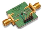
Figure 11 is a picture of a typical assembled evaluation board similar to the ones in the evaluation kits.
Figure 12. Typical Assembled Evaluation Board with SMA Connectors
MC13851 Advance Information, Rev. 2.0
20
Freescale Semiconductor
�Printed Circuit and Bill of Materials
Figure 13. 1575-, 1960-, 2140-, 2400 MHz Application Board
The bill of materials for each of the application frequency circuit boards is listed in Table 10. The value,
case size, manufacturer and circuit function of each component are shown.
Table 10. Bill of Materials for the Application Circuit Boards
Component
Value
Case
Manufacturer
Comments
1575 MHz Application Circuit (see Figure 7)
C1
22 pF
402
Murata
DC block, input match
C2
1 pF
402
Murata
DC block, output match
C3
33 pF
402
Murata
RF bypass
C4
0.1 μF
402
Murata
Low frequency bypass
L1
4.7 nH
402
Murata
Input match
L2
5.1 nH
402
Murata
Output match, bias decouple
L3
270 nH
402
Murata
Bias couple to logic
R1
1.2 kΩ
402
KOA
R2
10 Ω
402
KOA
Stability
R3
150 Ω
402
KOA
L2 de-Q, gain adjust
Bias set point
1900 MHz Application Circuit (see Figure 8)
C1
2.4pF
C2
0.9 pF
C3
33 pF
C4
.01 μF
L1
402
Murata
Input match
402
Murata
Output match
402
Murata
RF bypass
805
Murata
Low frequency bypass
5.1 nH
402
Murata
Input match
L2
3.3 nH
402
Murata
Output match
L3
270 nH
402
Murata
Bias couple to logic
R1
1.2 kΩ
402
KOA
LNA bias
R2
15 Ω
402
KOA
Stability
R3
620
402
KOA
De-Q L2, adjust gain, RLs
MC13851 Advance Information, Rev. 2.0
Freescale Semiconductor
21
�Scattering and Noise Parameters
Table 10. Bill of Materials for the Application Circuit Boards (continued)
Component
Value
Case
Manufacturer
Comments
2140 MHz Application Circuit (see Figure 9)
C1
2.4pF
402
Murata
Input match
C2
0.9 pF
402
Murata
Output match
C3
33 pF
402
Murata
RF bypass
C4
.01 μF
805
Murata
Low frequency bypass
L1
4.7 nH
402
Murata
Input match
L2
2.7
402
Murata
Output match
L3
270 nH
402
Murata
Bias couple to logic
R1
1.2 kΩ
402
KOA
R2
10 Ω
402
KOA
Stability
R3
620
402
KOA
De-Q L2, adjust gain, RLs
LNA bias
2400 MHz Application Circuit (see Figure 10)
5
C1
2.4pF
C2
0.9 pF
C3
33 pF
C4
.01 μF
L1
402
Murata
Input match
402
Murata
Output match
402
Murata
RF bypass
805
Murata
Low frequency bypass
3.6 nH
402
Murata
Input match
L2
2
402
Murata
Output match
L3
270 nH
402
Murata
Bias couple to logic
R1
1.2 kΩ
402
KOA
LNA bias
R2
10 Ω
402
KOA
Stability
R3
620
402
KOA
De-Q L2, adjust gain, RLs
Scattering and Noise Parameters
Table 11 through Table 14 list the S parameters for the packaged part in a 50 Ω system for each of the
modes of operation and for two values of the external bias resistor.
Table 11. Scattering Parameters, Active Mode, Rbias=1.2kΩ
(Vcc = 2.75V, 25°C, 50 Ω system)
S11
S21
S12
S22
f (MHz)
Mag
Ang
Mag
Ang
Mag
Ang
Mag
Ang
1000
0.712
-19.7
10.508
145.3
0.027
94.1
0.913
9.6
1050
0.696
-20.3
10.318
144.3
0.029
94.3
0.904
10.0
1100
0.679
-21.2
10.132
143.1
0.030
94.8
0.896
10.5
1150
0.663
-21.7
9.947
142.2
0.031
94.8
0.886
10.7
1200
0.651
-21.9
9.742
141.0
0.033
95.1
0.875
10.8
1250
0.634
-22.2
9.552
140.2
0.034
95.6
0.870
11.0
1300
0.619
-22.4
9.413
139.3
0.035
96.4
0.861
11.2
MC13851 Advance Information, Rev. 2.0
22
Freescale Semiconductor
�Scattering and Noise Parameters
Table 11. Scattering Parameters, Active Mode, Rbias=1.2kΩ (continued)
(Vcc = 2.75V, 25°C, 50 Ω system)
S11
S21
S12
S22
f (MHz)
Mag
Ang
Mag
Ang
Mag
Ang
Mag
Ang
1350
0.607
-22.9
9.242
138.3
0.036
97.3
0.854
11.5
1400
0.597
-23.3
9.069
138.0
0.038
98.5
0.851
11.6
1450
0.587
-23.6
8.977
137.0
0.040
99.3
0.847
11.4
1500
0.576
-23.9
8.813
136.2
0.042
100.3
0.845
11.1
1550
0.571
-24.4
8.806
135.9
0.044
101.5
0.846
10.2
1600
0.571
-26.2
8.693
134.7
0.049
100.1
0.840
8.2
1650
0.556
-28.2
8.583
133.0
0.050
97.4
0.802
7.2
1700
0.538
-29.7
8.420
131.8
0.051
96.5
0.779
7.4
1750
0.519
-31.3
8.284
130.8
0.052
96.4
0.764
7.2
1800
0.505
-33.5
8.129
129.5
0.054
96.1
0.751
6.8
1850
0.486
-35.7
8.009
128.3
0.057
95.2
0.737
5.6
1900
0.448
-37.5
7.735
126.4
0.058
91.7
0.700
5.2
1950
0.435
-37.8
7.564
126.2
0.058
92.2
0.688
5.5
2000
0.415
-41.7
7.421
124.4
0.061
90.4
0.662
4.1
2050
0.376
-45.4
7.155
122.5
0.063
86.6
0.618
3.7
2100
0.313
-44.8
6.708
121.6
0.059
80.1
0.569
6.2
2150
0.28
-37.0
6.321
121.8
0.052
79.7
0.541
11.7
2200
0.251
-29.5
5.956
125.2
0.044
78.1
0.561
18.1
2250
0.309
-16.2
6.073
130.1
0.037
100.5
0.648
20.3
2300
0.367
-24.7
6.554
129.3
0.050
110.1
0.694
14.8
2350
0.364
-30.5
6.756
126.9
0.058
108.1
0.678
9.3
2400
0.351
-35.0
6.542
124.4
0.062
104.0
0.648
8.3
2450
0.338
-37.9
6.459
122.8
0.065
102.4
0.627
7.8
2500
0.323
-40.5
6.304
121.6
0.066
100.3
0.613
8.1
2550
0.319
-41.4
6.168
120.6
0.067
100.7
0.608
8.1
2600
0.308
-43.6
6.047
119.6
0.068
99.4
0.606
7.1
Table 12. Scattering Parameters, Active Mode, Rbias=1.5kΩ
(Vcc = 2.75V, 25°C, 50 Ω system)
S11
S21
S12
S22
f (MHz)
Mag
Ang
Mag
Ang
Mag
Ang
Mag
Ang
1000
0.754
-17.9
9.171
150.9
0.028
94.9
0.941
10.7
1050
0.739
-18.6
9.055
149.8
0.029
95.2
0.933
11.1
1100
0.721
-19.4
8.902
148.7
0.031
95.0
0.927
11.7
1150
0.709
-19.9
8.774
147.9
0.032
95.4
0.918
11.8
1200
0.698
-20.3
8.629
146.8
0.033
95.6
0.910
12.0
1250
0.682
-20.6
8.517
146.2
0.035
96.3
0.907
12.2
MC13851 Advance Information, Rev. 2.0
Freescale Semiconductor
23
�Scattering and Noise Parameters
Table 12. Scattering Parameters, Active Mode, Rbias=1.5kΩ (continued)
(Vcc = 2.75V, 25°C, 50 Ω system)
S11
S21
S12
S22
f (MHz)
Mag
Ang
Mag
Ang
Mag
Ang
Mag
Ang
1300
0.667
-21.2
8.444
145.1
0.036
96.3
0.897
12.2
1350
0.654
-21.9
8.318
144.0
0.037
96.4
0.888
12.4
1400
0.640
-22.5
8.150
143.8
0.039
97.1
0.884
12.6
1450
0.625
-22.8
8.093
142.6
0.040
97.3
0.876
12.6
1500
0.611
-23.0
7.908
141.9
0.041
97.6
0.871
12.6
1550
0.595
-23.1
7.910
141.3
0.043
98.2
0.863
12.2
1600
0.591
-23.1
7.668
140.8
0.044
98.5
0.861
11.8
1650
0.586
-24.0
7.619
139.9
0.046
99.0
0.841
11.5
1700
0.577
-25.1
7.505
139.2
0.048
99.0
0.829
11.8
1750
0.560
-26.7
7.410
138.5
0.049
99.1
0.821
11.9
1800
0.548
-28.0
7.283
137.6
0.050
99.4
0.813
11.7
1850
0.528
-28.8
7.154
136.9
0.052
99.6
0.807
11.5
1900
0.513
-28.8
7.006
136.3
0.053
98.7
0.794
11.4
1950
0.509
-29.0
6.929
136.3
0.054
99.8
0.789
11.5
2000
0.500
-31.2
6.861
135.6
0.056
100.1
0.781
11.1
2050
0.489
-32.4
6.832
134.8
0.058
101.1
0.773
10.7
2100
0.475
-33.9
6.707
134.5
0.060
100.5
0.770
10.2
2150
0.467
-34.2
6.660
133.1
0.062
101.1
0.750
9.6
2200
0.454
-37.8
6.588
133.3
0.063
99.6
0.745
9.2
2250
0.436
-39.4
6.538
132.1
0.065
100.1
0.730
8.6
2300
0.409
-41.7
6.508
130.5
0.066
98.0
0.714
8.4
2350
0.390
-40.9
6.467
129.7
0.067
98.2
0.693
7.3
2400
0.378
-41.5
6.181
128.3
0.067
97.2
0.671
8.6
2450
0.369
-42.2
6.079
127.5
0.068
97.5
0.659
9.7
2500
0.359
-43.2
5.945
126.8
0.068
97.6
0.651
10.7
2550
0.356
-44.0
5.825
126.3
0.069
97.8
0.652
11.4
2600
0.348
-44.7
5.680
125.7
0.069
98.1
0.652
11.9
Table 13. Scattering Parameters, Bypass Mode, Rbias=1.2kΩ and 1.5kΩ
(Vcc = 2.75V, 25°C, 50 Ω system)
S11
S21
S12
S22
f (MHz)
Mag
Ang
Mag
Ang
Mag
Ang
Mag
Ang
1000
0.356
-25.9
0.658
25.8
0.646
25.2
0.402
-12.4
1050
0.340
-24.6
0.663
24.9
0.651
24.3
0.387
-11.3
1100
0.327
-23.0
0.667
24.0
0.655
23.5
0.373
-9.9
1150
0.312
-21.4
0.671
23.3
0.659
22.7
0.359
-8.2
1200
0.298
-20.3
0.674
22.6
0.662
22.0
0.347
-6.5
MC13851 Advance Information, Rev. 2.0
24
Freescale Semiconductor
�Scattering and Noise Parameters
Table 13. Scattering Parameters, Bypass Mode, Rbias=1.2kΩ and 1.5kΩ (continued)
(Vcc = 2.75V, 25°C, 50 Ω system)
S11
S21
S12
S22
f (MHz)
Mag
Ang
Mag
Ang
Mag
Ang
Mag
Ang
1250
0.288
-18.7
0.677
21.8
0.665
21.4
0.336
-4.7
1300
0.275
-16.7
0.678
21.2
0.667
20.7
0.326
-3.4
1350
0.263
-14.8
0.679
20.6
0.668
20.1
0.318
-1.9
1400
0.253
-12.6
0.678
20.0
0.667
19.6
0.311
-0.7
1450
0.248
-10.0
0.675
19.9
0.664
19.5
0.306
-0.3
1500
0.250
-9.6
0.680
20.0
0.669
19.6
0.289
0.9
1550
0.244
-10.4
0.687
19.5
0.676
19.1
0.279
2.1
1600
0.235
-10.0
0.689
18.9
0.678
18.5
0.272
3.7
1650
0.226
-10.2
0.690
18.5
0.680
18.0
0.267
4.9
1700
0.220
-9.5
0.690
17.8
0.680
17.3
0.260
6.3
1750
0.211
-8.5
0.689
17.4
0.679
17.0
0.253
6.9
1800
0.197
-6.2
0.685
16.9
0.675
16.4
0.245
6.8
1850
0.199
-1.7
0.682
17.3
0.673
16.9
0.235
7.3
1900
0.202
-3.2
0.688
17.0
0.679
16.6
0.229
8.5
1950
0.194
-5.0
0.688
16.5
0.678
16.1
0.223
9.4
2000
0.186
-4.4
0.687
16.1
0.677
15.8
0.213
8.4
2050
0.182
-3.6
0.682
16.2
0.673
15.8
0.204
8.1
2100
0.180
-4.2
0.686
16.3
0.676
15.9
0.198
9.5
2150
0.185
-4.3
0.689
16.2
0.680
15.9
0.192
11.2
2200
0.185
-5.5
0.695
15.7
0.685
15.4
0.186
10.4
2250
0.187
-8.3
0.695
15.2
0.685
14.9
0.185
9.3
2300
0.186
-10.1
0.697
14.6
0.688
14.3
0.178
7.5
2350
0.185
-12.0
0.694
14.2
0.685
13.8
0.173
7.0
2400
0.181
-14.1
0.696
13.7
0.686
13.4
0.168
4.1
2450
0.178
-16.8
0.695
13.1
0.681
12.5
0.159
2.0
2500
0.177
-19.8
0.694
12.5
0.680
11.9
0.155
-1.7
2550
0.174
-23.6
0.691
11.8
0.677
11.2
0.150
-5.6
2600
0.171
-27.4
0.686
11.2
0.673
10.6
0.143
-9.1
Table 14. Scattering Parameters, Standby Mode, Rbias=1.2kΩ and 1.5kΩ
(Vcc = 2.75V, 25°C, 50 Ω system)
S11
S21
S12
S22
f (MHz)
Mag
Ang
Mag
Ang
Mag
Ang
Mag
Ang
1000
0.939
2.1
0.031
104.0
0.031
103.1
0.991
12.9
1050
0.935
2.2
0.033
104.4
0.033
103.8
0.990
13.3
1100
0.934
2.5
0.035
104.8
0.034
104.2
0.988
13.5
1150
0.931
2.7
0.037
105.2
0.036
104.4
0.986
14.0
MC13851 Advance Information, Rev. 2.0
Freescale Semiconductor
25
�Scattering and Noise Parameters
Table 14. Scattering Parameters, Standby Mode, Rbias=1.2kΩ and 1.5kΩ (continued)
(Vcc = 2.75V, 25°C, 50 Ω system)
S11
S21
S12
S22
f (MHz)
Mag
Ang
Mag
Ang
Mag
Ang
Mag
Ang
1200
0.926
2.7
0.039
105.4
0.038
104.7
0.985
14.5
1250
0.924
2.6
0.041
105.8
0.040
105.2
0.982
15.0
1300
0.920
2.8
0.043
105.8
0.042
105.3
0.978
15.0
1350
0.914
2.9
0.045
106.1
0.044
105.5
0.977
15.2
1400
0.906
2.9
0.047
106.4
0.046
105.9
0.974
15.5
1450
0.896
3.3
0.048
106.9
0.048
106.2
0.973
15.7
1500
0.901
3.7
0.051
108.4
0.050
107.8
0.969
16.0
1550
0.907
3.3
0.054
108.6
0.053
107.9
0.965
15.9
1600
0.904
2.9
0.056
108.4
0.056
108.0
0.964
15.9
1650
0.900
2.4
0.059
108.8
0.058
108.3
0.959
16.1
1700
0.896
1.7
0.061
109.2
0.061
108.6
0.957
16.2
1750
0.886
1.3
0.064
109.7
0.063
109.2
0.954
16.1
1800
0.871
1.1
0.068
111.0
0.067
110.4
0.948
15.7
1850
0.859
2.3
0.074
109.8
0.073
109.4
0.946
15.7
1900
0.871
2.1
0.075
108.1
0.074
107.5
0.941
15.4
1950
0.866
1.0
0.078
109.2
0.076
108.7
0.935
15.3
2000
0.855
0.4
0.081
109.1
0.080
108.9
0.929
15.0
2050
0.843
0.5
0.086
110.1
0.085
109.8
0.923
14.3
2100
0.844
0.3
0.093
108.8
0.092
108.4
0.920
14.2
2150
0.848
-0.2
0.100
106.5
0.099
106.0
0.916
14.0
2200
0.853
-0.9
0.103
103.2
0.101
102.8
0.911
13.2
2250
0.853
-2.1
0.105
101.6
0.104
101.0
0.907
12.4
2300
0.850
-3.1
0.106
99.8
0.105
99.4
0.901
11.6
2350
0.844
-3.9
0.110
99.2
0.109
98.7
0.891
10.8
2400
0.838
-5.1
0.113
97.0
0.111
96.4
0.887
9.9
2450
0.829
-6.5
0.116
96.2
0.114
95.2
0.877
8.9
2500
0.820
-7.9
0.119
93.5
0.117
92.6
0.867
7.6
2550
0.807
-9.4
0.122
91.3
0.120
90.6
0.858
6.1
2600
0.791
-11.2
0.125
88.1
0.122
87.4
0.840
4.9
Table 15 provides the active mode noise parameters when the bias resistor is 1.2 kΩ.
Table 15. Active Mode Noise Parameters, Rbias=1.2kΩ
(Vcc = 2.75V, 25 0C, 50 Ω system, Icc=4.6 mA)
Freq
(MHz)
Fmin
(dB)
Gamma Opt
Rn
Mag
Angle
Ga
(dB)
1000
0.91
0.329
-8.8
14.0
27.42
1200
0.92
7.000
-7.3
13.5
25.09
MC13851 Advance Information, Rev. 2.0
26
Freescale Semiconductor
�Scattering and Noise Parameters
Table 15. Active Mode Noise Parameters, Rbias=1.2kΩ (continued)
(Vcc = 2.75V, 25 0C, 50 Ω system, Icc=4.6 mA)
Freq
(MHz)
Fmin
(dB)
Gamma Opt
Ga
(dB)
Rn
Mag
Angle
1500
0.96
0.279
-12.3
12.5
22.83
1700
0.99
0.244
-17.2
12
21.43
1900
1.02
0.206
-20.8
11.5
20.15
2000
1.04
0.186
-21.5
11.5
19.57
2100
1.06
0.167
-20.9
11.0
19.04
2400
1.13
0.114
-9.6
11.0
17.74
2500
1.15
0.100
-1.6
10.5
17.43
2600
1.18
0.087
8.8
10.5
17.18
Table 16 provides the active mode noise parameters when the bias resistor is 1.5 kΩ.
Table 16. Active Mode Noise Parameters, Rbias=1.5kΩ
(Vcc = 2.75V, 25°C, 50 Ω system, Icc=3.3 mA)
Freq
(MHz)
Fmin
(dB)
Gamma Opt
Rn
Mag
Angle
Ga
(dB)
1000
0.92
0.358
-8.3
14.5
26.42
1200
0.93
0.344
-8.7
14.0
24.84
1500
0.97
0.306
-12.5
13.5
22.78
1700
1.00
0.273
-15.2
13.0
21.59
1900
1.04
0.237
-16.6
12.0
20.53
2000
1.06
0.218
-16.4
12.0
20.03
2100
1.08
0.199
-15.4
12.0
19.57
2400
1.16
0.143
-5.5
11.5
18.30
2500
1.19
0.127
0.6
11.5
17.91
2600
1.23
0.111
8.3
11.5
17.53
MC13851 Advance Information, Rev. 2.0
Freescale Semiconductor
27
�Scattering and Noise Parameters
Figure 14 through Figure 21 are the constant noise figure and gain circles with input and output stability
regions shown on Smith charts. Gamma opt, noise resistance and stability at the frequency are shown for
two values of the external bias resistor at 1600-, 1950-, 2150- and 2400 MHz.
Figure 14. Constant Noise Figure and Gain Circles, 1600 MHz, Rbias=1.2 kΩ
Figure 15. Constant Noise Figure and Gain Circles, 1600 MHz, Rbias=1.5kΩ
MC13851 Advance Information, Rev. 2.0
28
Freescale Semiconductor
�Scattering and Noise Parameters
Figure 16. Constant Noise Figure and Gain Circles, 1960 MHz, Rbias=1.2 kΩ
Figure 17. Constant Noise Figure and Gain Circles, 1960 MHz, Rbias=1.5kΩ
MC13851 Advance Information, Rev. 2.0
Freescale Semiconductor
29
�Scattering and Noise Parameters
Figure 18. Constant Noise Figure and Gain Circles, 2140 MHz, Rbias=1.2 kΩ
Figure 19. Constant Noise Figure and Gain Circles, 2140 MHz, Rbias=1.5kΩ
MC13851 Advance Information, Rev. 2.0
30
Freescale Semiconductor
�Scattering and Noise Parameters
Figure 20. Constant Noise Figure and Gain Circles, 2400 MHz, Rbias=1.2 kΩ
Figure 21. Constant Noise Figure and Gain Circles, 2400 MHz, Rbias=1.5kΩ
MC13851 Advance Information, Rev. 2.0
Freescale Semiconductor
31
�Packaging
6
Packaging
Figure 22 and Figure 22 are the package drawings with dimensions for the MLPD-8, 2 × 2 × 0.6 mm,
package.
DETAIL G
(See Figure 23)
Figure 22. Outline Dimensions for MLPD-8
MC13851 Advance Information, Rev. 2.0
32
Freescale Semiconductor
�Product Documentation
Figure 23. Package Details
7
Product Documentation
This data sheet is labeled as a particular type: Product Preview, Advance Information, or Technical Data.
Definitions of these types are available at: http://www.freescale.com.
8
Revision History
Table 17 summarizes revisions to this document since the previous release (Rev. 1).
Table 17. Revision History
Location
Revision
Throughout document
Changed package from MLF8 to MLPD-8
Section 2, “Electrical Specifications
Complete revision
Section 3, “Application Information
Complete update to Application Information
Section 3.4, “2400 MHz Application
New 2400 MHz content.
Section 4, “Printed Circuit and Bill of Materials
Complete update to MLPD-8 package.
Section 5, “Scattering and Noise Parameters
Added section and all content.
MC13851 Advance Information, Rev. 2.0
Freescale Semiconductor
33
�How to Reach Us:
Home Page:
www.freescale.com
Web Support:
http://www.freescale.com/support
USA/Europe or Locations Not Listed:
Freescale Semiconductor, Inc.
Technical Information Center, EL516
2100 East Elliot Road
Tempe, Arizona 85284
1-800-521-6274 or +1-480-768-2130
www.freescale.com/support
Europe, Middle East, and Africa:
Freescale Halbleiter Deutschland GmbH
Technical Information Center
Schatzbogen 7
81829 Muenchen, Germany
+44 1296 380 456 (English)
+46 8 52200080 (English)
+49 89 92103 559 (German)
+33 1 69 35 48 48 (French)
www.freescale.com/support
Japan:
Freescale Semiconductor Japan Ltd.
Headquarters
ARCO Tower 15F
1-8-1, Shimo-Meguro, Meguro-ku,
Tokyo 153-0064
Japan
0120 191014 or +81 3 5437 9125
support.japan@freescale.com
Asia/Pacific:
Freescale Semiconductor China Ltd.
Exchange Building 23F
No. 118 Jianguo Road
Chaoyang District
Beijing 100022
China
+86 10 5879 8000
support.asia@freescale.com
For Literature Requests Only:
Freescale Semiconductor Literature Distribution Center
1-800-441-2447 or +1-303-675-2140
Fax: +1-303-675-2150
LDCForFreescaleSemiconductor@hibbertgroup.com
Document Number: MC13851
Rev. 2.0
12/2010
Information in this document is provided solely to enable system and software
implementers to use Freescale Semiconductor products. There are no express or
implied copyright licenses granted hereunder to design or fabricate any integrated
circuits or integrated circuits based on the information in this document.
Freescale Semiconductor reserves the right to make changes without further notice to
any products herein. Freescale Semiconductor makes no warranty, representation or
guarantee regarding the suitability of its products for any particular purpose, nor does
Freescale Semiconductor assume any liability arising out of the application or use of any
product or circuit, and specifically disclaims any and all liability, including without
limitation consequential or incidental damages. “Typical” parameters that may be
provided in Freescale Semiconductor data sheets and/or specifications can and do vary
in different applications and actual performance may vary over time. All operating
parameters, including “Typicals”, must be validated for each customer application by
customer’s technical experts. Freescale Semiconductor does not convey any license
under its patent rights nor the rights of others. Freescale Semiconductor products are
not designed, intended, or authorized for use as components in systems intended for
surgical implant into the body, or other applications intended to support or sustain life,
or for any other application in which the failure of the Freescale Semiconductor product
could create a situation where personal injury or death may occur. Should Buyer
purchase or use Freescale Semiconductor products for any such unintended or
unauthorized application, Buyer shall indemnify and hold Freescale Semiconductor and
its officers, employees, subsidiaries, affiliates, and distributors harmless against all
claims, costs, damages, and expenses, and reasonable attorney fees arising out of,
directly or indirectly, any claim of personal injury or death associated with such
unintended or unauthorized use, even if such claim alleges that Freescale
Semiconductor was negligent regarding the design or manufacture of the part.
Freescale™ and the Freescale logo are trademarks of Freescale Semiconductor, Inc.
All other product or service names are the property of their respective owners.
© Freescale Semiconductor, Inc. 2006-2010. All rights reserved.
RoHS-compliant and/or Pb-free versions of Freescale products have the functionality
and electrical characteristics as their non-RoHS-compliant and/or non-Pb-free
counterparts. For further information, see http://www.freescale.com or contact your
Freescale sales representative.
For information on Freescale’s Environmental Products program, go to
http://www.freescale.com/epp.
�