MOTOROLA
Freescale Semiconductor, Inc.
Semiconductor Products Sector
MC145423
ABSOLUTE MAXIMUM RATINGS (Voltage Referenced to VSS)
Rating
Symbol
Value
Unit
VDD – VSS
–0.5 to 6
V
Voltage, Any Pin to VSS
V
–0.5 to VDD + 0.5
V
DC Current, Any Pin (Excluding
VDD, VSS)
I
±10
mA
TA
–40 to 85
°C
Tstg
–85 to 150
°C
DC Supply Voltage
Operating Temperature
Freescale Semiconductor, Inc...
Storage Temperature
This device contains circuitry to protect
the inputs against damage due to high static
voltages or electric fields; however, it is
advised that normal precautions be taken
to avoid applications of any voltage higher
than maximum rated voltages to this highimpedance circuit. For proper operation, it
is recommended that Vin and Vout be
to the range
VSS ≤ (Vin or Vout)
Pinconstrained
Selectable
Master/Slave
.
≤ VDD. Reliability of operation
is enhanced
C toModem
Limited
if unused Distance
inputs are
an appropriate
Ntied
I
logic level (e.g.,
R,either VSS or VDD).
Product Preview
Universal Digital Loop
Transceiver (UDLT-3)
The MC145423
TO is a CMOS integrated circuit designed
C
of the major
U building blocks in digital subscriber voice/da
D
telephone
systems and remote data acquisition and contro
RECOMMENDED OPERATING CONDITIONS (TA = –40° to 85°C) N
O
The
UDLT-3
incorporates into one device, all the funct
Parameter
Pins
Min
Typ
Max
Unit
ICthe
MC145421 (ISDN UDLT-2 master), MC145425 (ISDN
M
DC Supply Voltage
VDD SE
4.5
— (UDLT-1 5.5
slave),
MC145422
master), andV MC145426 (UD
E
Power Dissipation (PD = VDD)
VDD = 5 V
VDD
—
—
80
mW
slave).
AL
C
Since
these
modes/functions
are
pin
selectable, the MC
VDD = 5 V S VDD
—
—
80
mW
Power Dissipation (PD = VSS)
E
can
switch
E
Frame Rate
MSI
7.9be used in telephone
8.0
8.1 line cards,
kHz as well as rem
R
telsets
or
data
terminals.
F
CCI CLK Frequency (MSI = 8 kHz)
CCI
MHz
• —VDD = 4.52.048
V to 5.5 V
BY
UDLT-1 (CCI = 256 x MSI)
—
UDLT-2
8.192
• —28-Pin SOIC
and TSSOP8.29
Packages
ED
V
I
•
Protocol
Independent
Frame Rate Slip*
—
—
0.25
%
H
C
•
Pin
Controlled
Power-Down
Data Clock Rate (Master Mode)
TDC-RDC
kHz
AR
• 64LI Sensitivity—Control in 4100
Master Mode
UDLT-1
•128
2.048 MHz Output
in Slave
Mode
UDLT-2
—
4100
SDCLK (UDLT-2 Only)
Modulation Baud Rate
UDLT-1
UDLT-2
16
—
UDLT-2 Features
4100
LO1, LO2
kHz
kHz
• —Synchronous—Full Duplex256
160 kbps Voice and Data
—
— in a 2B+2D
512 Format for ISDN Compa
Communications
* The slave’s crystal frequency divided by 512 (UDLT-1) or 1024 (UDLT-2), must equal•theProvides
master’s MSI
frequency
±0.25%
for optimum
CCITT
Basic
Access
Data Transfer Rate (2B+
operation.
ISDNs on a Single Twisted Pair Up to 1 km on 26 AW
Larger Cable
UDLT-1 Features
• Pin Controlled Loopback
• Automatic Power-Up/Down (Slave)
• Full Duplex Synchronous 64 kbps Voice/Data Channel
8 kbps Signaling Data Channels Over One 26 AWG Wi
to 2 km
This document contains information on a product under development. Motorola
reserves the right to change or discontinue this product without notice.
© Motorola, Inc., 2000. All rights reserved.
4
For More
Information On This Product,
TELECOMMUNICATIONS
Go to: www.freescale.com
�Freescale Semiconductor, Inc.
MC145423
PIN ASSIGNMENT
Freescale Semiconductor, Inc...
CH
R
A
ED
V
I
1
2
3
4
5
6
7
8
9
10
11
12
13
14
28
27
26
25
24
23
22
21
20
19
18
17
16
15
VDD
LO1
MASTER/SLAVE
LO1
LO2
LO2
Rx
RE2/BCLK
RE1/CLKOUT
LI SENS/2.048 MHz
TDC-RDC/XTALout
CCI/XTALin
MSI/TONE
EN1-TE1 CCI/XTALIn
(TDC-RDC)/
EN2-TE2/SIE/B1B2
XTALout
Tx
MODULATOR
VSS
Vref
LI
LB
VD
SDI1
SDI2
FRAME 10/20
SDCLK/8kHz
SDO1
SDO2
SE/(Mu/A)
PD
MOD TRI/SQ
BLOCK D
B1
B2
D1
D2
REGIST
LOGIC
C.
IN
,
OR
T
OSC
UC
D
N
O
IC
M
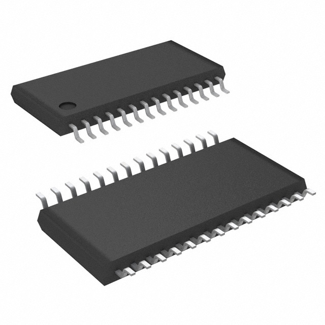
28-PIN SOIC/TSSOP PACKAGES
SE
LE
A
MSI/TONE
SC
E
E
MOD TRI/SQ
FR
FRAME 10/20
BY
CLKOUT
BCLK
Mu/A
SE
LATCH
SEQUENCE
AND
CONTROL
MASTER/
SLAVE
LI SENS/
2.048 MHz
SE
LATCH
SE
LATCH
TDC/RDC
VD
VD
CONTROL
LI
Vref
2
For More
Information On This Product,
TELECOMMUNICATIONS
Go to: www.freescale.com
DEMODULATOR
D2
REGISTER
LOGIC
D1
B2
B1
TELECOMMU
�Freescale Semiconductor, Inc.
MC145423
DIGITAL CHARACTERISTICS (VDD = 5 V ±10%, TA = –
Parameter
tp4
B18
Input High Level
Input Low Level
Input Current (Digital Pins)
B17
Input Current LI
Input Capacitance
B14
R
Tx Output HighO
Current
th1
CT
U
Tx Output
D Low Current
N
O
ICPD Output High Current — Slave Mode*
EM
B13
S
,
PD Output Low Current — Slave Mode*
B12
Tx, SDO1, SDO2, and VD Three-State Current
XTAL Output High Current
XTAL Output Low Current
B11
tsu5
HIGH IMPEDANCE
LE
A
SC
C
VALID
* To overdrive PD from a low level to 3.5 V, or a high level to 1.5 V requ
B18
ANALOG CHARACTERISTICS (VDD = 5 V ±10%, TA =
Parameter
Modulation Differential Amplitude (RL = 440 Ω)
B17
tp2
CH
R
A
ED
V
I
BY
EE
R
F
tp3
tw(L)
tw(H)
Freescale Semiconductor, Inc...
B15
B16
Output High Current (Excluding
. Tx and PD)
Output Current Low (Excluding
Tx and PD)
IN
Modulation Differential Offset
B16
Vref Voltage, Typically 9/20 x (VDD – VSS)
PCM Tone Level
DON’T CARE
Demodulator Input Impedance (LI to Vref)
* The input level into the demodulator to reliably demodulate incoming
tdly3
VD
tp6
SDO1,
SDO2
SDI1,
SDI2
Rx
tsu6
B11
Tx
RE1
TE1
BCLK
tp1
th2
B12
B13
tp5
B14
B15
Demodulator Input Amplitude*
Figure 1. UDLT-1 Slave Timing Nonsynchronous
8
For More
Information On This Product,
TELECOMMUNICATIONS
Go to: www.freescale.com
TELECOMMU
�Freescale Semiconductor, Inc.
MC145423
MASTER SWITCHING CHARACTERISTICS (VDD = 5 V ±10%, TASLAVE
= –40° toSWITCHING
85°C, CL = 50 CHARACTERISTICS
pF)
(VDD = 5
Figure
No.
Parameter
Input Rise Time: All Digital Inputs
Min
Max
Parameter
tr Rise Time: —
2
Input
All Digital Inputs
tf Fall Time: All
— Digital Inputs2
Input
Input Fall Time: All Digital Inputs
Pulse Width:
TDC, RDC, RE1, RE2, MSI, SDCLK (UDLT-2)
CCI Duty Cycle
Propagation Delay:
MSI to SDO1, SDO2, VD (PD = VDD)
TDC to Tx
MSI, TE1, TE2, RE1, RE2 to TDC-RDC Setup Time
Freescale Semiconductor, Inc...
F
Symbol
TDC-RDC to MSI, TE1, TE2, RE1, RE2, Hold Time
Rx to TDC-RDC Setup Time
Rx to TDC-RDC Hold Time
SDI1, SDI2 to MSI Setup Time
SDI1, SDI2 to MSI Hold Time
MSI Rising Edge to First SDCLK Falling Edge
(UDLT-2 Only)
EE
R
F
LE
A
SC
SE
Unit
µs
µs
tp Output Pulse Width: BCLK
ns
Clock
90
—
Crystal Frequency
tw2(H,L)
45
55
%
Propagation Delay Times: .
tPLH,
ns
CRising to BCLK (TONE
EN1, EN2, TE1
= VDD)
tPHL
— IN
50
EN1, EN2,
TE1 Rising to BCLK (TONE = VSS)
,
—
50
BCLK to EN1, EN2, TE1 Falling
OR
T
tsu3
20
ns (UDLT-1)
RE1—Rising to BCLK
C
U
RE150
Falling to BCLK
DD) (UDLT-1)
th5 D
—(TONE = Vns
RE1 Falling to BCLK (TONE = VSS) (UDLT-1)
N
tO
30
—
ns BCLK to Tx
ICsu5
TE1,TE2 tons
SDO1, SDO2
30
—
M th1
Rx
to BCLK Setup
tsu2
30 Time
th2to BCLK Hold30
Rx
Time
—
ns
—
ns
tSDI1,
P1LH SDI2 to TE—Setup Time 50
ns
V
TE1,TE2 Falling Edge to Tx High IImpedance
SDI1, SDI2 to TE Hold Time
tsu6
—
50
ns
EN1, EN2 Rising Edge to DCLK Rising Edge (UDLT-2)
tsu7
—
50
ns
EN1, EN2 Rising Edge to First Tx Data Bit Valid
tdly
—
70
ns
BCLK Rising Edge to Tx Data Bits 2 – 8 Valid
tsu8
—
135
ns
DCLK Pulse Width High (UDLT-2)
SDI1, SDI2 Data Setup (Data Valid Before SDCLK
Falling Edge) (UDLT-2 Only)
tsu9 Pulse Width
50 Low (UDLT-2)
—
DCLK
TE Rising Edge to First Tx Data Bit Valid
BY
TDC-RDC Rising Edge to Tx Data Bits D
2 – 8 Valid
H
E
SDCLK Rising Edge to SDO1,
RCSDO2 Bit Valid
A
(UDLT-2 Only)
SDI1, SDI2 Data Hold (Data Valid After SDCLK
Falling Edge) (UDLT-2 Only)
PD, LB Setup (PD, LB Valid Before MSI Rising Edge)
PD, LB Hold (PD, LB Valid After MSI Rising Edge)
ns
DCLK Rising Edge to SDO1, SDO2 (UDLT-2)
th3
20
—
ns
SDI1, SDI2 Setup (SDI1, SDI2 Valid Before DCLK
Falling Edge) (UDLT-2)
tsu10
50
—
ns
SDI1, SDI2 Hold (SDI1, SDI2 Valid After DCLK
th4
20
—
ns
Falling
Edge) (UDLT-2)
EN1, TE1 Rising Edge to VD Valid
SE PIN TIMING
F
Parameter
LB, PD Hold
(LB, PD Valid After SE Falling Edge)
SDO1, SDO2, VD High Impedance After SE Falling Edge
SDO1, SDO2, VD Valid After SE Rising Edge
LB, PD Setup
(LB, PD Valid Before SE Rising Edge)
6
For More
Information On This Product,
TELECOMMUNICATIONS
Go to: www.freescale.com
TELECOMMU
�12
Figure 5. UDLT-2 Master Timing
For More
Information On This Product,
TELECOMMUNICATIONS
Go to: www.freescale.com
Tx
RE1
TE1
PD/LB
BCLK
VALID
B1
B11
tp1
tsu10
th4
B12
tPLH/tPHL
DON’T CARE
B13
tp5
tsu9
B14
B1
B15
B1
th3
B16
B17
tp2
B11
tp
B14
B18
DON’T CARE
tsu8
B17
tw(L)
B14
B18
B15
tw2
HIGH IMPEDANCE
tp3
VALID
B13
B16
DON’T CARE
B12
th1
B15
tsu7
B16
tdly
tw2
tw(H)
B2
B17
B18
B2
R,
O
CT
U
ND
tw2
C
IN
VD
SDI1,
SDI2
tPLH
dly3 /tPHL
tsu5
B13
th5
tw2
S
O
IC
EM
SDO1,
SDO2
B12
tsu3
LE
A
SC
SDCLK
tP1LH
B11
tsu6
th5
BY
EE
R
F
Rx
th5
ED
V
I
RE1/
RE2
Tx
th5
CH
R
A
TE1/TE2
TDC/RDC
MSI
tp
Freescale Semiconductor, Inc...
tp4
DON’T CARE
MC145423
Freescale Semiconductor, Inc.
.
Figure 2. UDLT-1 Slave
TELECOMMU
�10
Figure 3. UDLT-2 Slave Timing
For More
Information On This Product,
TELECOMMUNICATIONS
Go to: www.freescale.com
th5
B11
tPLH/tPHL
tsu3
B12
th5
th3
B13
B14
B17
tp
tsu3
B15
B18
B18
VALID
B16
tdly2
B21
B21
B22
B23
B17
B22
tw(H)
B23
B24
B24
B18
tw2
B25
B25
tw2
B2
B2
B26
B26
tw(L)
B11
B28
B27
th5
B11
B28
B1
B27
HIGH IMPEDANCE
.
RE1
Tx
TE1
tsu3
tp
B1
B16
B17
C
IN
CCI,
TDC/
RDC
tdly3
B1
B15
B16
R,
O
CT
U
ND
VD
MSI
SDI1,
SDI2
tsu9
B14
B15
tw(L)
O
IC
EM
SDO1,
SDO2
th1
B13
B14
tsu7
S
SDCLK
B12
tsu5
B13
tdly1
tp1
EE
R
F
LE
A
SC
tPHL
B11
Rx
B12
tp2
BY
B11
tp5
ED
V
I
Tx
EN2
tp1
CH
R
A
EN1
BCLK
tw(H)
Freescale Semiconductor, Inc...
MC145423
Freescale Semiconductor, Inc.
Figure 4. UDLT-1
TELECOMMU
�Freescale Semiconductor, Inc.
MC145423
MC145423 UDLT-3 PIN STATES FOR UDLT-1 SLAVE MODE (continued)
Freescale Semiconductor, Inc...
MC145423
Pin
No.
Pin
Name
23
UDLT-1 Slave Mode Powered-Down
UDLT-1 Slave Mode
Powered-Up
SE
TONE = 0, Off
TONE = 1, On
No Valid
Burst Rec’d
Valid
Burst Rec’d
No Valid
Burst Rec’d
Valid
Burst Rec’d
BCLK =
128 kHz
BCLK =
128 kHz
BCLK =
128 kHz
In/out
Normal
LB Low
RE2/
BCLK
Output
BCLK =
128 kHz
BCLK = 0
BCLK =
128 kHz
24
Rx
Input
64 kbps
Data In
Don’t Care
Don’t Care
Don’t Care SDO1,
Don’t
Care
SDO2, VD
.
Don’t Care
25
LO2
Output
Modulator
Out
Modulator
Out
LO2 = LO1
,LO2 = LO1
LO2 = LO1
26
LO1
Output
Modulator
Out
Modulator
Out
LO1 = LO2
OR
T
LO1U
=C
LO2
LO1 = LO2
D
N
27
MASTER/
SLAVE
Input
1
1
1
28
VDD
Power
+V
+V
LE
A
SC
LO2 = LO1
O
IC
EM
S+V
LB, PD
IN
C
th
PREVIO
INTERNAL
tdly1
Figure
LO1 = LO2
1
1
1
+V
+V
+V
6. SE
MC145423 UDLT-3 PIN STATES FOR UDLT-1
EE MASTER MODE
MC145423
BY
FRUDLT-1 Master Mode
ED
V
In/out
Normal
HI
C
Power Supply
R
APower
Gnd
Pin
No.
Pin
Name
1
VSS
2
Vref
Analog
Ref
3
LI
4
UDLT-1 Master Mode
Powered-Down
Powered-Up
LB Low
SE Low
Normal
SE Low
Power Supply
Gnd
Power Supply
Gnd
Power Supply
Gnd
Power Supply
Gnd
AGND VDD/2
AGND VDD/2
AGND VDD/2
AGND VDD/2
AGND VDD/2
Input
Analog In
Don’t Care
Analog In
Analog In
Analog In
LB
Input
1
0
State Latched
Don’t Care
Don’t Care
5
VD
Output
Digital out
Digital out
High Impedance
Digital out
High Impedance
6
SDI1
Input
8 kbps Data In
8 kbps Data In
State Latched
8 kbps Data In
State Latched
7
SDI2
Input
8 kbps Data In
8 kbps Data In
State Latched
8 kbps Data In
State Latched
8
FRAME 10/20
Input
0
0
0
0
0
9
SDCLK
10
SDO1
Output
8 kbps Data Out 8 kbps Data Out High Impedance 8 kbps Data Out High Impedance
11
SDO2
Output
8 kbps Data Out 8 kbps Data Out High Impedance 8 kbps Data Out High Impedance
12
SE/(Mu/A)
Input
1
1
0
1
0
13
PD
Input
1
1
State Latched
0
State Latched
14
MOD
TRI/SQ
Input
0
0
0
0
0
15
Tx
Output
64 kbps
Data Out
64 kbps
Data Out
64 kbps
Data Out
64 kbps
Data Out
64 kbps
Data Out
16
EN2-TE2/
SIE/B1B2
Input
SIE Digital In
SIE Digital In
SIE Digital In
SIE Digital In
SIE Digital In
16
Don’t Care High Impedance High Impedance High Impedance High Impedance High Impedance
For More
Information On This Product,
TELECOMMUNICATIONS
Go to: www.freescale.com
TELECOMMU
�Freescale Semiconductor, Inc.
MC145423
SOIC PACKAGE PINOUT COMPARISON
MC145423 UDLT-3 PIN STATES FOR UDLT-1 SLAV
UDLT-3 PINOUT VERSUS MC145421DW/22DW/25DW/26DW
(UDLT-1/UDLT-2 MASTER/SLAVE) PINOUT
Freescale Semiconductor, Inc...
UDLT-3
MC145423
UDLT-1 Master
MC145422
UDLT-1 Slave
MC145426
Pin
No.
Pin
Name
Pin
No.
Pin
Name
Pin
No.
Pin
Name
1
VSS
1
VSS
1
VSS
2
Vref
2
Vref
2
Vref
3
LI
3
LI
3
LI
4
LB
5
LB
5
LB
5
VD
6
VD
6
VD
6
SDI1
7
SI1
7
SI1
7
SDI2
9
SI2
9
8
FRAME 10/20
Logic 0
9
SDCLK/8kHz
High Impedance
10
SDO1
8
SO1
11
SDO2
10
SO2
12
SE/(Mu/A)
11
13
PD
14
MOD TRI/SQ
15
Tx
16
BY
EDSE
V
I PD
CH Logic 0
R
A
12
R, Input3
O
44
Input4
CLBTLB
U
55ND VD
VD
5
Output
O
D1I
SDI1
Input6
IC 66
M
7
D2I
7
E
33
S
SI2
Logic
LE0
A
SCSDCLK
UDLT-1 Slave Mode
MC145423
Powered-Up
UDLT-2 Master
UDLT-2 Slave
Pin
Pin
MC145421
MC145425
No.
Name
In/out
Normal
LB Low
Pin
Pin
Pin
Pin
1
VSS
Power
Power Supply Power Supply
No.
Name
No.
Name
Gnd
Gnd
1
VSS
1
VSS
2
Vref
Analog.
AGND
AGND
C
2
Vref
Vref
Ref 2
VDD
/2
VDD/2
N
I
7
SO2
109
10
Output
D2O
SDCLK/8kHz
11
Mu/A
12
PD
11
10
12
D2O
SDCLK/
8kHz
SE
SDO1
PD
11
Output
12
(Mu/A)
8 kbps
PD
Data Out
Logic 1
8 kbps
DataTx
Out
Logic 0
Tx
Logic 1
SDO2
Tx
14
12
TE2
SE/(Mu/A)
EN1-TE1
15
TE1
14
TE1
15
13
18
MSI/TONE
13
MSI
13
(Tone) TE
16
14
19
CCI/XTALin
17
CCI
16
(XTALin) X1
20
TDC-RDC/
XTALout
18
TDC/RDC
17
(XTALout) X2
17
15
18
21
LI SENS/
2.048 MHz
22
RE1/CLKOUT
23
RE2/BCLK
24
Rx
19
25
LO2
26
LO1
27
MASTER/
SLAVE
14
15
11
13
17
B1B2
Logic 0
Logic 0
LI SENS
2.048 MHz Out
16
17
19
18
20
20
RE1
18
(BCLK) CLK
Rx
19
Rx
22
LO2
22
LO2
21
19
22
23
LO1
23
LO1
23
20
21
Logic 0
24
VDD
Input
10
SIE
VDD
DI1
8 kbps
Data In
DI2
8 kbps
Logic 1
Data In
DCLK
0
D1O
SO1
14
28
VD
Digital
Out
8
Input
9
EN2-TE2/SIE/
B1B2
High Impedance
1LB
DCLK
FRAME
D1O
10/20
Tx
RE1
SDI2
Logic 1
LI In
Analog
8
8
9
E8E
R
F
16
20
LI LI
Logic 1
24
VDD
24
22
TE1
PD
Output
13
0
Digital Out
8 kbps
Data In
8 kbps
Data In
0
SDCLK/8kHz
8 kbps
Data Out
8 kbps
Data Out
14
Input
1=EN2
Mu,
0=A
I/O15
EN1
1
1
TONE
0
0
(XTALin) CCI
64 kbps
(XTALout) XTL
Data Out
64 kbps
Data Out
MSI
16
MOD
Input
TRI/SQ
CCI
17
Tx
Output
TDC/RDC
18
EN2-TE2/
Logic 0
SIE/B1B2
LI SENS
EN1-TE1
RE1
MSI/
RE2
TONE
Rx
CCI/
LO2
XTAL
in
Analog In
Input
1/0 B1B2
2.048 MHz Out
1= Mu,
0=A
1/0 B1B2
Output
19
Input
20
EN1 = 8 kHz
CLKOUT
1/0 TONE
BCLK
21
Input
22
Rx
XTALin
4.096LO2
MHz
LO1
TDC-RDC/
XTALout
Logic 0
23
Output
LI SENS/
2.048 MHz
VDD
RE1/
CLKOUT
Output
LO1
XTAL
out
4.096 MHz
Logic 1
2.048 MHz
2.048 MHz
24
Output
VDD
RE1 = 8 kHz
RE1 = 8 kHz
For More
Information On This Product,
TELECOMMUNICATIONS
Go to: www.freescale.com
EN1 = 8 kHz
1/0 TONE
XTALin
4.096 MHz
XTALout
4.096 MHz
TELECOMMU
�Freescale Semiconductor, Inc.
MC145423
PIN DESCRIPTIONS
VSS
Negative Supply (Pin 1)
This is the most negative power pin, and should be
tied to system ground (0 V).
Freescale Semiconductor, Inc...
Vref
Voltage Reference Output (Pin 2)
This is the output from the internal reference supply
(mid-supply) and should be bypassed to both VSS and
VDD with 0.1 µF capacitors. This pin usually serves
as an analog ground reference for transformer
coupling of the device’s incoming bursts from the line.
No external load should be placed on this pin.
LI
Line Input (Pin 3)
CT
21
Input
Digital In
ULI SENS/
SDI1 and SDI2
D
2.048 MHz
LI Sensitivity
N
D ChannelOSignaling
Data Bit Inputs 1 and 2
22
RE1/
Input
RE1 8 kHz
C 7)
(Pins 6Iand
EM
IV
H
LB
RC
A
Loopback Low Input (Pin 4)
Master Mode: A low on this pin ties the internal
modulator output to the internal demodulator input,
which loops the entire burst for testing purposes.
During the loopback operation, the LI input is ignored,
and the LO1 and LO2 outputs are driven to equal
voltages. The state of the LB pin is internally latched if
the SE pin is held low. This feature is only active when
the PD input is high.
Slave Mode: When this pin is low and PD is high,
the incoming B channels from the master are burst
back to the master, instead of the Rx B channel input
data. The SDI1 and SDI2 functions operate normally
in this mode, and the BCLK (pin 23) is held low.
Additionally, for both the UDLT-1 and UDLT-2 mode,
when the TONE (pin 18) and loopback functions are
active simultaneously, the loopback function overrides
the TONE function.
VD
Valid Data Output (Pin 5)
A high level on this pin indicates that a valid line
transmission has been demodulated. A valid line
transmission burst is determined by proper
Digit
LI Sen
RE1 8
CLKOUT
These
inputs are the
SMaster Mode (UDLT-1):
RE2/
Don’t Care High Impedance
E8 kbps serial23data inputs
in
UDLT-1
mode.
Data on
L
A these pins is loaded onBCLK
the rising edge of MSI for
C
S
24
Rx
Input
64 kbps Data In
This pin is the input to the demodulator for the
E
E
incoming bursts. This input has an internal 240
kΩ
R
F
resistor tied to the Vref pin, so an external capacitor
or
Y
line transformer may be used to couple B
the input signal
to the device with no dc offset. ED
20
synchronization
and the
absencePIN
of detected
bitFOR
errors.
MC145423
UDLT-3
STATES
UDLT-1 MAS
VD is a CMOS output and is high impedance when SE UDLT-1 Ma
is low.
MC145423
Power
Master Mode: VD changes state on the rising
Pin
Pin
edge of MSI,
when PD
is high. When
PD is low,
VD
No.
Name
In/out
Normal
LB L
changes state at the end of demodulation of a
EN1-TE1
Input
TE1 8
transmission17burst and
does not change
again TE1
until8 kHz
18 edges
MSI/TONE
Inputat which
MSI
8 kHz
MSI 8
three MSI rising
have occurred,
time
it
goes low, or19
until the next
a burst.
CCI/ demodulation
Input of CCI
2.048 MHz CCI 2.04
.
Slave Mode: If no
transmissions
from
the
master
XTAL
in
NC250 µs, as
I
have been received
within the
last
20
TDC-RDC/
Input
TDC-RDC
TDC,
R
determined by an internal
oscillator,
VD
will
go
low.
XTAL
Data
Clk
Data
Oout
High Imp
64 kbps
transmission to the slave. The state of these pins is
LO2
Output
Modulator Out
LO2 =
latched if SE25is held low.
Slave Mode
inputs areModulator
the
26 (UDLT-1):
LO1 These
Output
Out
LO1 =
8 kbps serial27data inputs
in
UDLT-1
mode.
Data
on
MASTER/
Input
0
0
these pins is loaded on
the rising edge of TE1 for
SLAVE
transmission to the master. If no transmissions from
28
VDD
Power
+V
+V
the master are being received
and PD is high, data on
these pins will be loaded into the part on an internal
signal. Therefore,
dataUDLT-3
on these PIN
pins STATES
should be FOR
steadyUDLT-2 SLAV
MC145423
until synchronous communication with the master has
been established, as indicated by the high on VD.
Master Mode (UDLT-2): These inputsUDLT-2
are the Slave Mode
MC145423
Powered-Up
16 kbps serial data inputs in UDLT-2 mode. Two
bits
Pin
Pin
should be clocked into each of these inputs between
No. of the
Name
In/out
the rising edges
MSI frame
referenceNormal
clock. The LB Low
1 D channel
VSS is clocked
Power into
Power
first bit of each
an Supply Power Supply
Gnd
intermediate buffer on the first falling edge Gnd
of the
SDCLK following
the
of MSI. AGND
The second AGND
2
Vrefrising edge
Analog
VDD/2
VDD/2
bit of each D channel is clockedRef
in on the next
negative transition
of
the
SDCLK.
If
further
SDCLK
3
LI
Input
Analog In
Analog In
negative edges occur, new information is serially
Input
1
0
4
LB
clocked into the buffer replacing the previous data,
5
VD
Output bitsDigital
Out to Digital Out
one bit at a time.
Buffered
D channel
are burst
the slave on 6the nextSDI1
rising edge
of the MSI
Input
16 frame
kbps
16 kbps
Data In if SE Data In
reference clock. The state of these pins is latched
is held low. 7
SDI2
Input
16 kbps
16 kbps
In
Data In
Slave Mode (UDLT-2): These inputs Data
are the
16 kbps serial
data
inputs
in
UDLT-2
mode.
The
D
8
FRAME
Input
1
1
channel data bits are10/20
clocked in serially on the
negative edge
of the
16 kbps SDCLK
output
pin.
9
SDCLK
Output
16 kHz
16 kHz
For More
Information On This Product,
TELECOMMUNICATIONS
Go to: www.freescale.com
TELECOMMU
�Freescale Semiconductor, Inc.
MC145423
MC145423 UDLT-3 PIN STATES FOR UDLT-2 SLAVE MODE (continued)
MC145423 UDLT-3 PIN STATES FOR UDLT-2 MAS
UDLT-2 Slave Mode
Powered-Up
MC145423
Freescale Semiconductor, Inc...
UDLT-2
Slave Mode
MC145423
UDLT-2 Maste
Powered-Down
Pin
Pin
TONE =
0, Off Name
TONE = 1, On Normal
No.
In/out
LB L
Pin
No.
Pin
Name
In/out
Normal
LB Low
No Valid
Burst Rec’d
10
SDO1
Output
16 kbps
Data Out
16 kbps
Data Out
Data Not
Changed
11
SDO2
Output
16 kbps
Data Out
16 kbps
Data Out
Data Not
Changed
12
SE/
(Mu/A)
Input
1/0
Mu/A
1/0
Mu/A
1/0
Mu/A
13
PD
I/O
1
1
14
MOD
TRI/SQ
Input
1
1
15
Tx
Output
128 kbps
Data Out*
16
EN2-TE2/
SIE/B1B2
Output
EN2 8 kHz
17
EN1-TE1
Output
18
MSI/
TONE
Input
EN1 8 kHzY
B
1/0 Tone
D
E
IV
Input CH XTAL
AR 8.192 MHz
19
CCI/
XTALin
20
TDC-RDC/
XTALout
Output
21
LI SENS/
2.048 MHz
22
1/0 Tone
No Valid
Power
Burst Rec’d
Data
Not Ref
2 16 kbpsVref
Analog
Data Out
Changed
3
LI
Input
.
16 kbps
DataCNot
4
LB
Input
N
Data Out
I
, Changed
5
VD R
Output
1/0
1/0
O
T
6 Mu/A
Input
Mu/A
CSDI1
U
7 D 0 SDI2
0
N
O
10/
1
1
IC 8 FRAME
20
M
E
SHigh
EImpedance
L
CA EN2 = 0
EN2 8 S
kHz
EE
R
FEN1 8 kHz
EN1 = 0
128 kbps
Data Out*
1 ValidVSS
Burst Rec’d
0 No Tone
9 64 kbps
SDCLK
Data
Out
10
SDO1
11
XTAL
8.192 MHz
XTAL
8.192 MHz
XTAL
8.192 MHz
XTAL
8.192 MHz
Output
2.048 MHz
2.048 MHz
2.048 MHz
RE1/
CLKOUT
Output
RE1 8 kHz
RE1 8 kHz
RE1 0
23
RE2/
BCLK
Output
BCLK
128 kHz
BCLK = 0
BCLK
128 kHz
24
Rx
Input
128 kbps
Data In
Don’t Care
Don’t Care
25
LO2
Output
Modulator
Out
Modulator
Out
26
LO1
Output
Modulator
Out
27
MASTER/
SLAVE
Input
28
VDD
Power
1 Input
Power
Gn
16
kbpsVDD/2
AGND
Data Out
Analog In
16 kbps
1
Data Out
Digital Out
1/0
16Mu/A
kbps Data In
16 kbps
16 kbps
0 Data In
16 kbps
1 1
AGND
Don’t
0
Digita
1
EN2 = 0
Input
500 Hz
ToneOutput
Out
EN2 8 kHz
50016
HzkHz
Tone
Out Data
16 kbps
Out
EN2 8 kHz
16 kbp
Ou
SDO2
EN1 = 0
Output
EN1 8 kHz
16 kbps Data
Out
EN1 8 kHz
16 kbp
Ou
120 NoSE/(Mu/A)
Input
Tone
1 No Tone
13
XTAL
8.192 MHz
0 Input
Valid Supply
Power
Burst Rec’d
Gnd
PD
Input
1 Tone1
1
16 k
1
1
14 XTAL
MOD TRI/SQ XTAL
Input
8.192 MHz
8.192 MHz
15
Tx
Output
XTAL
XTAL
8.192 MHz
8.192 MHz
16
EN2-TE2/
Input
2.048SIE/B1B2
MHz
2.048 MHz
XTAL1
8.192 MHz
128 kbps*
XTAL
Data Out
8.192 MHz
TE2 8 kHz
2.048 MHz
17
EN1-TE1
Input
RE1 0
RE1 8 kHz
18
MSI/TONE
Input
TE1 8 kHz
RE1 8 kHz
8 kHz
TE1 8
19
CCI
BCLK
4.096 MHz
128 kHz
TDC-RDC
128Data
kbpsClk
Data In
Digital In
LO2Sensitivity
= LO1
CC
4.096
LO2 = LO1
CCI/XTALin
Input
BCLK
BCLK
128 kHz
128 kHz
Input
20
TDC-RDC/
Don’t Care
XTALout 128 kbps
Data In
21
LI SENS/
Input
LO2 =
LO1 MHzLO2 = LO1
2.048
Modulator
Out
LO2 = LO1
22
RE1/
Input
LO2 =CLKOUT
LO1
LO1 = LO2
RE1 8 kHz
LO1 = LO2
RE1 8
23
1
1
1
RE2 8 kHz
RE2 8
1
128 kbps Data In 128 kbps
+V
+V
+V
* Tx is high impedance when TE1 and TE2 are both low, simultaneously.
Tx is undefined when TE1 and TE2 are both high, simultaneously.
24
25
26
RE2/BCLK
1
Rx
+V LO2
LO1
Input
1
Input
Output
+V
Output
Modulator
Out
+V
Modulator Out
1
128 k
Data
TE2 8
8k
TDCData
Digit
Sens
LO2 =
LO1 =
27
MASTER/
SLAVE
Input
0
0
28
VDD
Power
+V
+V
* Tx is high impedance when TE1 and TE2 are both low, simultaneous
Tx is undefined when TE1 and TE2 are both high, simultaneously.
18
For More
Information On This Product,
TELECOMMUNICATIONS
Go to: www.freescale.com
TELECOMMU
�MC145423
Freescale Semiconductor, Inc.
which is simultaneous
with the transfer of the transmit
FRAME 10/20
word. See(Pin
the pin
8) descriptions for EN2-TE2/SIE/
B1B2 and EN1-TE2 for more information.
The UDLT series of transceivers are designed to
Master Mode (UDLT-2): B channel data is input
operate using a ping-pong transmission scheme with
on this pin and controlled by the RE1, RE2, and TDCan 8 kHz burst rate. Each frame the master device
RDC pins.
“pings” a burst of data to the slave, which responds
Slave Mode (UDLT-2): This pin is an input for
with a “pong” burst of data. This pin selects whether
the B channel data. B channel 1 data is clocked in on
this 8 kHz frame will have a 10-bit data burst for
the first eight falling edges of the BCLK output
UDLT-1 compatibility or .a 20-bit data burst for
following the rising edge of the EN1
C output. B channel
UDLT-2 compatibility.
Neight
RE2/BCLK
I
2 data is clocked in on the next
edges of
, selectsfalling
A logic low (0RV)
the UDLT-1 (MC145422/
Receive Data Enable Input 2 or B Channel
the BCLK following theOrising edge of the EN2
MC145426)T
mode. This sets the device to operate with
Data Clock Output (Pin 23)
output.
C
one 64 kbps
voice/data
channel and two 8 kbps
U
D
Master Mode (UDLT-1): This pin is high
signaling
N channels. A logic high (VDD) on this pin
LO2
O
impedance.
selects
the UDLT-2
(MC145421/MC145425) mode.
Line Drive
(Pin 25)
IC Output
Master Mode (RE2 UDLT-2): See pin
M
This
sets
the
device
to operate with two 64 kbps
E LO2 pin, along with LO1
(pin 26) form
a pushdescription for RE1 (pin 22).
SThe
channels and two 16 kbps
(2B+2D).
Epull output, to drive the twisted pair channels
Slave Mode (BCLK UDLT-1 and UDLT-2):
transmission line.
L
drives the twisted pair with a 10-bit,
This output provides the data clock for the telset
SDCLK
CA The UDLT-1
S
E
256
kHz
modified
DPSK
(MDPSK)
burst,
or a square
codec-filter. This clock signal is 128 kHz and begins
D
Channel
Signaling
Data
Clock
Input (Pin 9)
E
R
wave (set by pin 14 MOD TRI/SQ) burst, each 125 µs.
operating upon the successful demodulationFof a burst
Master Mode (UDLT-2): This is the transmit and
Y high and
The UDLT-2 drives the twisted pair with a 20-bit
from the master. At this time, EN1-TE1Bgoes
receive data clock input for both D channels. See
512 kHz modulated burst. When these pins are idle
BCLK starts toggling. BCLK remains
D active for
SDO1 and SDO2 pin descriptions for more
VE it remains low
and set for square wave modulation, they rest at the
16 periods, at the end of whichItime
information.
Hfrom the master. In this
positive power supply voltage. When these pins are
until another burst is received
C
Master Mode (UDLT-1): High impedance.
idle and set for MDPSK, they rest at Vref. For power
manner, synchronization
ARbetween the master and slave
Slave Mode (UDLT-2): This is the transmit and
supply voltages less than 4.5 V, squarewave
is established and any clock slippage is absorbed each
receive data clock output for both D channels. It starts
modulation must be used.
frame. If TONE (pin 18) is brought high, then EN1on demodulation of a burst from the master device.
TE1/RE1 are generated from an internal oscillator
This signal is rising-edge aligned with the EN1 and
LO1
until TONE is brought low, or an incoming burst from
BCLK
signals.
After
Line Driver
Output
(Pin
26)the demodulation of a burst, the
the master is received. BCLK is disabled when LB is
SDCLK line completes two cycles and then remains
held low.
See thelow
pin until
description
LO2from
(pinthe
25).master is
the nextfor
burst
demodulated. In this manner, synchronization with the
Rx
MASTER/SLAVE
master is established and any clock slip between
Receive Data Input (Pin 24)
Master/Slave Mode (Pin 27)
master and slave is absorbed each frame.
Master Mode (UDLT-1): The 8-bit B channel
A logic low
(0 V)Mode
on this(UDLT-1):
pin selectsThis
master
a 8 kHz
Slave
pin and
outputs
data is clocked into the device on this pin, on the
logic highequivalent
(VDD) selects
slave.
to TE1.
falling edges of TDC-RDC, under the control of RE1.
VDD
Slave Mode (UDLT-1): The 8-bit B channel data
SDO1 and SDO2
PositiveDSupply
(Pin
28)
from the telset PCM codec-filter is input on this pin on
Channel
Signaling
Data Outputs 1 and 2
the eight falling edges of BCLK after RE1 goes high,
(Pins 10 and 11)
This is the most positive power supply pin.
when EN2-TE2/SIE/B1B2, pin 16 is low. When EN2Acceptable operating
voltages
are from These
4.5 V to
5.5 V.
Master Mode
(UDLT-2):
serial
outputs
TE2/SIE/B1B2, pin16 is high, the receive data word is
provide the 16 kbps D channel signaling information
latched in during the high period of EN1-TE1, pin 17
from the incoming burst. Two data bits should be
clocked out of each of these two outputs between the
rising edges of the MSI frame reference clock. The
rising edge of MSI produces the first bit of each
D channel on its respective pin. Circuitry then
searches for a negative D channel clock edge. This
Freescale Semiconductor, Inc...
data buffer with data from the Rx pin on the next eight
falling edges of the TDC-RDC clock. The RE1 and
RE2 enables should be roughly leading edge aligned
with the TDC-RDC data clock. These enables are
rising edge sensitive and need not be high for the
entire B channel input period.
Slave Mode (CLKOUT UDLT-2): This pin
serves as a buffered output of the crystal frequency
divided by two.
24
For More
Information On This Product,
TELECOMMUNICATIONS
Go to: www.freescale.com
TELECOMMU
�MC145423
Freescale Semiconductor, Inc.
Freescale Semiconductor, Inc...
250 µs have elapsed without a burst from the master
being successfully demodulated. This allows the slave
device to self power-up and power-down in demand
powered loop systems. When held low, the device
powers down and the only active circuitry, is that
which is necessary for the demodulation of data. When
held high, the device is powered up and transmits
normally in response to received bursts from the
master.
of the incoming
wordupdated
at the Rx
beedge
transmitted
pin is also
on pin
the will
rising
of the EN1
to the slave.
The PCM word to the slave will have LSB
signal.
forced low in this mode. In this manner, signal bit 2 to/
MSI/TONE
from the slave
UDLT is inserted into the PCM words
Sync
Inputfrom
or Tone
Enable Input
the masterMaster
sends and
receives
the backplane,
for
(Pin
18)
routing through the PABX for simultaneous voice/data
communication.
The Mode
state of(MSI):
this pinThis
is internally
Master
pin is the master 8 kHz
latched if frame
the SEreference
pin is brought
low.
input. and
Theheld
rising
edge of MSI loads
Slave B
Mode
(UDLT-1):
In
this
mode,
this
is during the
and D channel data, which had beenpin
input
.
an input and
selects
the
timeslot
used
for
transferring
previous frame, into theCmodulator section of the
N pin
MOD TRI/SQ
Ithe
the receive
data word.
When, this
is low, burst
the device
device,
and initiates
outbound
onto the
Modulation Select (Pin 14)
R
uses the RE1
pin pair
timing
the
same
as
the
MC145426
twisted
cable.
The
rising
edge
of
MSI
also
O
T
UDLT-1
slave.
When
this
pin
is
a
logic
1,
the
receive
Cbuffering of the B and D channel data
A logic low (0 V) on this pin selects the MDPSK
initiates the
word is latched
inU
during
the TE1
timeslot, frame. MSI should
D
modulation which has a slew controlled voltage output
demodulated
during
the previous
N
simultaneously
with
the
transmit
word
for reduced EMI/RFI. This output looks like a triangle
beOapproximately leading edgetransfer.
alignedThe
with the TDCC
I
RE1 pin timing
is not
affected
by
this selection.
waveform that is modulated with different angles for
RDC
data
clock
input
signal.
EM Mode
UDLT-2):
In this
mode,
Slave(EN2-TE2
Mode (TONE):
the peaks. A logic high (VDD) on this pin, selects
A high
on this
pin causes a
SMaster
E
this
pin
functions
as
EN2-TE2.
This
pin,
along
with
square wave output for maximum power to the line.
500 Hz square wave PCM tone to be inserted in place
L
the outputdata.
of data
forfeature
their allows the
of control
the demodulated
This
CA TE1 pin-17
S
Tx
respectivedesigner
B-channel
on the Tx
output
pin. When
both keyboard
to provide
audio
feedback
for telset
EE
Transmit Data Output (Pin 15)
TE1 and TE2
are
low,
the
Tx
pin
is
high
impedance.
R
depressions.
F
The rising edge of the respective enable produces the
Y
Master Mode (UDLT-1): This pinB
is high
first bit ofCCI/XTAL
the selected
inB-channel data on the Tx pin.
D
impedance when TE1 is low. When
TE1
is high, this
E
Convert
Clock
Crystal
Input (Pin 19)
Internal circuitry
then
scansInput
for theornext
negative
IVdata on rising edges
pin presents new 8-bit B channel
H
transition
of
the
TDC-RDC
clock.
Following
this
Master Mode (CCI UDLT-1): A 2.048 MHz
of TDC-RDC.
RC
event, the next seven bits of the selected B-channel
A
Slave Mode (UDLT-1): B channel data is output
clock signal should be applied to this pin. This signal
data are output on the next seven rising edges of the
on this pin on the rising edge of BCLK, while TE1 is
is used for internal sequencing and control. This signal
TDC-RDC data clock. When TE1 and TE2 are high
high. This pin is high impedance when TE1 is low.
should be frequency and phase coherent with MSI for
simultaneously, data on the Tx pin is undefined. TE1
Master Mode (UDLT-2): This pin is high
optimum performance.
and TE2 should be approximately leading-edge
Slave Mode (XTALin UDLT-1): A 4.096 MHz
impedance when both TE1 and TE2 are low. This pin
aligned with the TDC-RDC data clock.
To keep the Tx
serves as an output for B channel information received
crystal is tied between this pin and XTALout (pin 20).
pin out of the high impedance state, these enable lines
from the slave device. The B channel data is under
A 10 MΩ resistor across this pin and XTAL
and
should be high while the respective B channel data is out
control of TE1 and TE2 and TDC-RDC.
25 pF capacitors from this pin and XTALout to VSS
being output.
Slave Mode (UDLT-2): This pin is an output for
are required for stability and to ensure start-up. This
Slave Mode (EN2-TE2 UDLT-2): Functioning as
the B channel data received from the master.
pin may be driven from an external source. XTALout
EN2-TE2, this pin is an output and serves as an 8 kHz
B channel 1 data is output on the first eight cycles of
should be left open if an external signal is used on this
enable signal for the input and output of the B channel
the BCLK output when EN1 is high. B channel 2 data
input.
2 data. While EN2 is high, B channel 2 data is clocked
Master Mode (CCI UDLT-2): An 8.192 MHz
is output on the next eight cycles of the BCLK, when
out on the Tx pin on the eight rising edges of the
clock should be supplied to this input. The 8.192 MHz
EN2 is high. B channel data bits are clocked out on the
BCLK. During this same time, B channel 2 input data
input should be 50% duty cycle. This signal may free
rising edge of the BCLK output pin.
is clocked in on the Rx pin, on the eight falling edges
run with respect to all other clocks without
of the BCLK.
EN2-TE2/SIE/B1B2
performance degradation.
B Channel 2 Enable Output or
EN1-TE1 Slave Mode (XTALin UDLT-2): Normally, an
Signal Insert Enable (Pin 16)
8.192
MHz crystal
is tied
between
B Channel
1 Enable
Output
(Pin
17) this pin and the
XTAL
(pin
20).
A
10
MΩ
resistor between
out
Master Mode (SIE UDLT-1): In this mode, this
This pin
is
the
logical
inverse
of
EN2-TE2,
and
XTALin and XTALout and 25 pF capacitors
from
pin functions as SIE. When held high, this pin causes
serves to control
B
channel
1
data.
See
the
above
pin to ensure
XTAL
and
XTAL
to
V
are
required
in
out
SS
signal bit 2, as received from the slave, to be inserted
description
for more
EN1 serves
as the
stability
andinformation.
start-up. XTAL
in may also be driven with
into the LSB of the outgoing PCM word at the Tx pin.
slave device’s
8 kHz 8.192
frame MHz
reference
signal.
The VD
an external
signal
if a crystal
is not
The SDI2 pin will be ignored, and in its place, the LSB
22
For More
Information On This Product,
TELECOMMUNICATIONS
Go to: www.freescale.com
TELECOMMU
�Freescale Semiconductor, Inc.
A
A
N = 0.5
B
D
TIP
DT SUFFIX
TSSOP PACKAGE
CASE 1168-01
N = 0.5
MC145423
b1
C
15
GAGE
PLANE
A1
θ°
0.25
L
N=2
110 Ω
MOD TRI/SQ
MASTER/SLAVE
LO1
LO2
5V
VD
SDCLK
SDO1
SDO2
MSI/TONE
2.048 MHz
CCI/XTAL
MC145423
UDLT-3
SLAVE
MODE
SDI2
75 kΩ
TI–
TI+
PO+
TG
28
For More
Information On This Product,
TELECOMMUNICATIONS
Go to: www.freescale.com
1 kΩ
1 kΩ
5V
68 µF
REC
5V
PO–
MC145484
VIEW A
A2
0.1 µF
(θ 1°)
MILLIMETERS
MIN
MAX
--1.20
0.05
0.15
0.80
1.05
0.19
0.30
0.19
0.25
0.09
0.20
0.09
0.16
9.60
9.80
0.65 BSC
6.40 BSC
4.30
4.50
0.50
0.70
0°
8°
14° REF
VSS
A
DIM
A
A1
A2
b
b1
c
c1
D
e
E
E1
L
θ
θ1
EN2-TE2 (I/O)/SIE
A
SEATING PLANE
0.01 µF
CH
R
SIDE
AVIEW
0.1 M
A
MCLK
VAG
VAG-REF
28X b
BY
0.2
5.
Rx
RE1/CLKout
RE2/BCLK
A
ED
V
IB C
EE
28X
R
F
4.
DIMENSIONS IN MILLIMETERS.
DIMENSION D DOES NOT INCLUDE MOLD
PROTRUSION. ALLOWABLE MOLD PROTRUSION IS
0.15 PER SIDE.
DIMENSION E1 DOES NOT INCLUDE INTERLEAD
FLASH OR MOLD PROTRUSION. INTERLEAD FLASH
OR PROTRUSION SHALL NOT EXCEED 0.25 PER
SIDE.
DIMENSION b DOES NOT INCLUDE DAMBAR
PROTRUSIONS. DAMBAR PROTRUSION SHALL NOT
CAUSE THE LEAD WIDTH TO EXCEED 0.38.
DT
(D)
S
2.
3.
PD
RO–
PI
0.05
LE
A
SC
O
IC
EM
LB
LI
Vref
TOP VIEW
PD
END
VIEW
VIEW A
FSR
C
Mu/A
B
VDD
A
Tx
EN1-TE1 (I/O)
0.2
2X 14 TIPS
e
DR
26X
VDD
e/2
5V
Freescale Semiconductor, Inc...
14
2X
BASIC DIGITAL TELSET
1
PIN 1
INDEX
5V
4.7 kΩ
R,
O
CT
NOTES:
U
1. DIMENSIONS AND TOLERANCING PER ASME
ND Y14.5M, 1994.
110 Ω
(b) .
C
N
I
SECTION
A-A
E1
SE/(Mu/A)
SDI1
4.7 kΩ
E/2
E
c1
N=4
c
FST
BCLKT
BCLKR
28
TELECOMMU
�Freescale Semiconductor, Inc.
MC145423
MULTICHANNEL DIGITAL LINE CARD
PACKAGE D
POWER
SUPPLY
DW SU
SOIC PA
CASE 7
Freescale Semiconductor, Inc...
SDO1
LE
A
SC
LB
VD
RING
POWER
SUPPLY
CH
R
A
TIP
ED
V
I
BY
EE
R
F
FRAME 10/20
VSS
M
B
M
.
0.25
R,
O
1
CT
U
B
PIN 1 IDENT
EN2-TE2(I/O)/SIE D
SE/(Mu/A) ON
IC
MASTER/SLAVE
M
MOD
SELECT
SE
UDLT-3 PD
MASTER RE1/CLKOUT
MODE EN1-TE1 (I/O)
SDO2
SDCLK
RE2/BCLK
LI SENS/2.048 MHz
C
IN
TO
BACKPLANE
H
CCI/XTALin
15
TRANSMIT DATA BUS
RECEIVE DATA BUS
2.048 MHz DATA CLOCK
14
A
SDI2
28
Rx
TDC/RDC/XTALout
LO2
LI
SDI1
D
8 kHz FRAME
SYNC
A
Tx
E
TIP
MSI/TONE
0.10
A1
VDD
LO1
Vref
e
B
C
0.025
M
C A
S
B
SEATING
PLANE
S
TO
BACKPLANE
VDD
LO1
Vref
LO2
LI
MSI/TONE
TIMING
AND
CONTROL
Tx
Rx
TDC/RDC/XTALout
CCI/XTALin
UDLT-3 PD
MASTER RE1/CLKOUT
MODE EN1-TE1 (I/O)
SDO1
EN2-TE2(I/O)/SIE
SDO2
SDI1
SDI2
SDCLK
RE2/BCLK
LI SENS/2.048 MHz
LB
VD
SE/(Mu/A)
MASTER/SLAVE
MOD SELECT
FRAME 10/20
VSS
RING
26
For More
Information On This Product,
TELECOMMUNICATIONS
Go to: www.freescale.com
TELECOMMU
�Freescale Semiconductor, Inc...
Freescale Semiconductor, Inc.
CH
R
A
ED
V
I
BY
EE
R
F
LE
A
SC
S
O
IC
EM
R,
O
CT
U
ND
MC145423
C
IN
.
Digital DNA is a trademark of Motorola, Inc.
Motorola reserves the right to make changes without further notice to any products herein. Motorola makes no warranty, representation or
guarantee regarding the suitability of its products for any particular purpose, nor does Motorola assume any liability arising out of the
application or use of any product or circuit, and specifically disclaims any and all liability, including without limitation consequential or
incidental damages. “Typical” parameters can and do vary in different applications and actual performance may vary over time. All operating
parameters, including “Typicals”, must be validated for each customer application by customer’s technical experts. Motorola does not
convey any license under its patent rights nor the rights of others. Motorola products are not designed, intended, or authorized for use as
components in systems intended for surgical implant into the body, or other applications intended to support or sustain life, or for any other
application in which the failure of the Motorola product could create a situation where personal injury or death may occur. Should Buyer
purchase or use Motorola products for any such unintended or unauthorized application, Buyer shall indemnify and hold Motorola and its
officers, employees, subsidiaries, affiliates, and distributors harmless against all claims, costs, damages, and expenses, and reasonable
attorney fees arising out of, directly or indirectly, any claim of personal injury or death associated with such unintended or unauthorized use,
even if such claim alleges that Motorola was negligent regarding the design or manufacture of the part. Motorola and
are registered
trademarks of Motorola, Inc. Motorola, Inc. is an Equal Opportunity/Affirmative Action Employer.
How to reach us:
USA/EUROPE/Locations Not Listed: Motorola Literature Distribution: P.O. Box 5405, Denver, Colorado 80217.
1-303-675-2140 or 1-800-441-2447
JAPAN: Motorola Japan Ltd.; SPS, Technical Information Center, 3-20-1 Minami-Azabu. Minato-ku, Tokyo 106-8573 Japan.
81-3-3440-3569
ASIA/PACIFIC: Motorola Semiconductors H.K. Ltd.; Silicon Harbour Centre, 2 Dai King Street, Tai Po Industrial Estate, Tao Po, N.T.,
Hong Kong. 852-26668334
TECHNICAL INFORMATION CENTER: 1-800-521-6274
HOME PAGE: http://motorola.com/semiconductors/
For More Information On This Product,
Go to: www.freescale.com
MC145423/D
�