MOTOROLA
Freescale Semiconductor, Inc.
SEMICONDUCTOR TECHNICAL DATA
Order this document
by MC145484/D
MC145484
Freescale Semiconductor, Inc...
5 V PCM Codec-Filter
The MC145484 is a general purpose per channel PCM Codec–Filter with pin
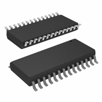
DW SUFFIX
selectable Mu–Law or A–Law companding, and is offered in 20–pin SOG,
20
SOG PACKAGE
SSOP, and TSSOP packages. This device performs the voice digitization and
CASE 751D
1
reconstruction as well as the band limiting and smoothing required for PCM
systems. This device is designed to operate in both synchronous and
.
asynchronous applications and contains an on–chip precision reference
C
SD SUFFIX
N
voltage.
I
SSOP
,
This device has an input operational amplifier whose output is the input to the
R
20
CASE 940C
encoder section. The encoder section immediately low–pass filters the analog
TO 1
C
signal with an active R–C filter to eliminate very high frequency noise from being
modulated down to the passband by the switched capacitor filter. From the
DU
N
active R–C filter, the analog signal is converted to a differential signal. From thisO
DT SUFFIX
point, all analog signal processing is done differentially. This allows processing
IC
TSSOP
M
of an analog signal that is twice the amplitude allowed by a single–ended
CASE
948E
E
20
S
design, which reduces the significance of noise to both the inverted
and
E
non–inverted signal paths. Another advantage of this differential
design is that
1
AL signal
noise injected via the power supplies is a common–mode
that is
C
S
cancelled when the inverted and non–inverted signals
are recombined. This
ORDERING INFORMATION
EE
dramatically improves the power supply rejectionR
ratio.
MC145484DW
SOG Package
After the differential converter, a differential F
switched capacitor filter band–
MC145484SD
SSOP
passes the analog signal from 200 Hz to 3400
BY Hz before the signal is digitized
MC145484DT
TSSOP
D
by the differential compressing A/D converter.
VEand expands it using a differential D/A
The decoder accepts PCM data
I
H is low–pass filtered at 3400 Hz and sinX/X
converter. The output of the D/A
Cswitched
R
compensated by a differential
capacitor filter. The signal is then filtered
PIN ASSIGNMENT
A
by an active R–C filter to eliminate the out–of–band energy of the switched
capacitor filter.
VAG
20
1
VAG Ref
The MC145484 PCM Codec–Filter has a high impedance VAG reference pin
TI+
19
2
ROwhich allows for decoupling of the internal circuitry that generates the
TI18
PI 3
mid–supply VAG reference voltage, to the VSS power supply ground. This
reduces clock noise on the analog circuitry when external analog signals are
TG
17
4
POreferenced to the power supply ground. This device is optimal for electronic
Mu/A
16
PO+
5
SLIC interfaces.
VSS
6
15
V
The MC145484 PCM Codec–Filter accepts a variety of clock formats,
DD
including Short Frame Sync, Long Frame Sync, IDL, and GCI timing
FST
14
FSR 7
environments. This device also maintains compatibility with Motorola’s family
DT
13
DR 8
of Telecommunication products, including the MC14LC5472 and MC145572
BCLKT
12
BCLKR 9
U–Interface Transceivers, MC145474/75 and MC145574 S/T–Interface Transc e i v e r s , M C 1 4 5 5 3 2 A D P C M Tr a n s c o d e r, M C 1 4 5 4 2 2 / 2 6 U D LT – 1 ,
11 MCLK
PDI 10
MC145421/25 UDLT–2, and MC3419/MC33120 SLICs.
The MC145484 PCM Codec–Filter utilizes CMOS due to its reliable
low–power performance and proven capability for complex analog/digital VLSI
functions.
•
•
•
•
•
•
•
•
•
Single 5 V Power Supply
Typical Power Dissipation of 15 mW, Power–Down of 0.01 mW
Fully–Differential Analog Circuit Design for Lowest Noise
Transmit Band–Pass and Receive Low–Pass Filters On–Chip
Active R–C Pre–Filtering and Post–Filtering
Mu–Law and A–Law Companding by Pin Selection
On–Chip Precision Reference Voltage of 1.575 V for a – 0 dBm TLP @ 600 Ω
Push–Pull 300 Ω Power Drivers with External Gain Adjust
MC14LC5480EVK is the Evaluation Kit for This Device
REV 2
3/98
TN98031100
Motorola, Inc. 1998
MOTOROLA
For More Information On This Product,
Go to: www.freescale.com
MC145484
1
�Freescale Semiconductor, Inc.
RECEIVE
SHIFT
RO -
DR
REGISTER
DAC
FREQ
PI
FSR
-
PO -
+
BCLKR
SHARED
DAC
Mu/A
-1
PO +
SEQUENCE
VDD
AND
VDD
VSS
1.575 V
REF
Freescale Semiconductor, Inc...
VAG Ref
1
R*
VSS
TG
TI TI +
+
.
PDI
CONTROL
R*
VAG
R,
O
CT
U
ND
C
IN
EE
R
F
FREQ
LE
A
SC
S
O
IC
EM
MCLK
BCLKT
FST
ADC
TRANSMIT
SHIFT
DT
BY
D
Figure
VE 1. MC145484 5 V PCM Codec–Filter Block Diagram
I
CH
R
A DESCRIPTION
which increment. When the chord bits increment, the step
DEVICE
A PCM Codec–Filter is used for digitizing and reconstructing the human voice. These devices are used primarily for
the telephone network to facilitate voice switching and transmission. Once the voice is digitized, it may be switched by
digital switching methods or transmitted long distance (T1,
microwave, satellites, etc.) without degradation. The name
codec is an acronym from ‘‘COder’’ for the analog–to–digital
converter (ADC) used to digitize voice, and ‘‘DECoder’’ for
the digital–to–analog converter (DAC) used for reconstructing voice. A codec is a single device that does both the ADC
and DAC conversions.
To digitize intelligible voice requires a signal–to–distortion
ratio of about 30 dB over a dynamic range of about 40 dB.
This may be accomplished with a linear 13–bit ADC and
DAC, but will far exceed the required signal–to–distortion
ratio at larger amplitudes than 40 dB below the peak amplitude. This excess performance is at the expense of data per
sample. Two methods of data reduction are implemented by
compressing the 13–bit linear scheme to companded
pseudo–logarithmic 8–bit schemes. The two companding
schemes are: Mu–255 Law, primarily in North America and
Japan; and A–Law, primarily used in Europe. These companding schemes are accepted world wide. These companding schemes follow a segmented or ‘‘piecewise–linear’’ curve
formatted as sign bit, three chord bits, and four step bits. For
a given chord, all sixteen of the steps have the same voltage
weighting. As the voltage of the analog input increases, the
four step bits increment and carry to the three chord bits
MC145484
2
REGISTER
bits double their voltage weighting. This results in an effective resolution of six bits (sign + chord + four step bits) across
a 42 dB dynamic range (seven chords above 0, by 6 dB per
chord).
In a sampling environment, Nyquist theory says that to
properly sample a continuous signal, it must be sampled at a
frequency higher than twice the signal’s highest frequency
component. Voice contains spectral energy above 3 kHz, but
its absence is not detrimental to intelligibility. To reduce the
digital data rate, which is proportional to the sampling rate, a
sample rate of 8 kHz was adopted, consistent with a bandwidth of 3 kHz. This sampling requires a low–pass filter to
limit the high frequency energy above 3 kHz from distorting
the in–band signal. The telephone line is also subject to
50/60 Hz power line coupling, which must be attenuated
from the signal by a high–pass filter before the analog–to–
digital converter.
The digital–to–analog conversion process reconstructs a
staircase version of the desired in–band signal, which has
spectral images of the in–band signal modulated about the
sample frequency and its harmonics. These spectral images
are called aliasing components, which need to be attenuated
to obtain the desired signal. The low–pass filter used to attenuate these aliasing components is typically called a reconstruction or smoothing filter.
The MC145484 PCM Codec–Filter has the codec, both
presampling and reconstruction filters, and a precision voltage reference on–chip.
For More Information On This Product,
Go to: www.freescale.com
MOTOROLA
�Freescale Semiconductor, Inc.
PIN DESCRIPTIONS
POWER SUPPLY
VDD
Positive Power Supply (Pin 6)
This is the most positive power supply and is typically connected to + 5 V. This pin should be decoupled to VSS with a
0.1 µF ceramic capacitor.
VSS
Negative Power Supply (Pin 15)
ANALOG INTERFACE
This is the most negative power supply and is typically
connected to 0 V.
TI+
Transmit Analog Input (Non–Inverting)
C. (Pin 19)
N
This is the non–inverting input
, I of the transmit input gain
setting operational amplifier.R
This pin accommodates a differO
ential to single–endedTcircuit for the input gain setting op
This output pin provides a mid–supply analog ground. This
C
amp. This allows input
signals that are referenced to the V SS
pin should be decoupled to VSS with a 0.01 µF ceramic
DU to the VAG pin with minimum noise.
pin to be levelNshifted
capacitor. All analog signal processing within this device is
O be connected to the VAG pin for an inverting
This pin C
may
referenced to this pin. If the audio signals to be processed
I configuration if the input signal
amplifier
is already referare referenced to V SS, then special precautions must be
M
E
enced
to
the
V
pin.
The
common
mode
range of the TI+
utilized to avoid noise between V SS and the VAG pin. Refer to
AG
S
and TI– pins is from 1.2 V, to VDD minus 1.2 V. This is an FET
the applications information in this document for more inE
L gate input.
formation. The VAG pin becomes high impedance when thisA
C
The TI+ pin also serves as a digital input control for the
device is in the powered–down mode.
S
E
transmit
input multiplexer. Connecting the TI+ pin to VDD will
E
R
VAG Ref
place
this
amplifier’s output (TG) into a high–impedance
F
Analog Ground Reference Bypass (Pin 1)Y
state, and selects the TG pin to serve as a high–impedance
B the on–chip cirinput to the transmit filter. Connecting the TI+ pin to VSS will
This pin is used to capacitively bypass
D
E
also
place this amplifier’s output (TG) into a high–impedance
cuitry that generates the mid–supply
voltage
for
the
V
outAG
V
I
state,
and selects the TI– pin to serve as a high–impedance
put pin. This pin should be bypassed
to
V
with
a
0.1
µF
SS
H
C
input to the transmit filter.
ceramic capacitor using short,
low
inductance
traces.
The
R
VAG Ref pin is only usedAfor generating the reference voltage
TI–
for the VAG pin. Nothing is to be connected to this pin in addiTransmit Analog Input (Inverting) (Pin 18)
tion to the bypass capacitor. All analog signal processing
within this device is referenced to the VAG pin. If the audio
This is the inverting input of the transmit gain setting opsignals to be processed are referenced to VSS, then special
erational amplifier. Gain setting resistors are usually conprecautions must be utilized to avoid noise between VSS and
nected from this pin to TG and from this pin to the analog
the VAG pin. Refer to the applications information in this
signal source. The common mode range of the TI+ and TI–
document for more information. When this device is in the
pins is from 1.2 V to VDD – 1.2 V. This is an FET gate input.
powered–down mode, the VAG Ref pin is pulled to the VDD
The TI– pin also serves as one of the transmit input multipower supply with a non–linear, high–impedance circuit.
plexer pins when the TI+ pin is connected to VSS. When TI+
is connected to VDD, this pin is ignored. See the pin descripCONTROL
tions for the TI+ and the TG pins for more information.
Mu/A
TG
Mu/A Law Select (Pin 16)
Transmit Gain (Pin 17)
This pin controls the compression for the encoder and the
expansion for the decoder. Mu–Law companding is selected
This is the output of the transmit gain setting operational
when this pin is connected to VDD and A–Law companding is
amplifier and the input to the transmit band–pass filter. This
selected when this pin is connected to VSS.
op amp is capable of driving a 2 kΩ load. Connecting the TI+
pin to VDD will place the TG pin into a high–impedance state,
PDI
and selects the TG pin to serve as a high–impedance input to
Power–Down Input (Pin 10)
the transmit filter. All signals at this pin are referenced to the
This pin puts the device into a low power dissipation mode
VAG pin. When TI+ is connected to VSS, this pin is ignored.
when a logic 0 is applied. When this device is powered down,
See the pin descriptions for the TI+ and TI– pins for more inall of the clocks are gated off and all bias currents are turned
formation. This pin is high impedance when the device is in
off, which causes RO–, PO–, PO+, TG, VAG, and DT to
the powered–down mode.
VAG
Analog Ground Output (Pin 20)
Freescale Semiconductor, Inc...
become high impedance and the VAG Ref pin is pulled to the
VDD power supply with a non–linear, high–impedance circuit.
The device will operate normally when a logic 1 is applied to
this pin. The device goes through a power–up sequence
when this pin is taken to a logic 1 state, which prevents the
DT PCM output from going low impedance for at least two
FST cycles. The VAG and VAG Ref circuits and the signal processing filters must settle out before the DT PCM output or
the RO– receive analog output will represent a valid analog
signal.
MOTOROLA
For More Information On This Product,
Go to: www.freescale.com
MC145484
3
�Freescale Semiconductor, Inc.
RO–
Receive Analog Output (Inverting) (Pin 2)
This is the inverting output of the receive smoothing filter
from the digital–to–analog converter. This output is capable
of driving a 2 kΩ load to 1.575 V peak referenced to the VAG
pin. If the device is operated half–channel with the FST pin
clocking and FSR pin held low, the receive filter input will be
conencted to the VAG voltage. This minimizes transients at
the RO– pin when full–channel operation is resumed by
clocking the FSR pin. This pin is high impedance when the
device is in the powered–down mode.
Freescale Semiconductor, Inc...
PI
Power Amplifier Input (Pin 3)
This is the inverting input to the PO– amplifier. The non–
inverting input to the PO– amplifier is internally tied to the
VAG pin. The PI and PO– pins are used with external resistors in an inverting op amp gain circuit to set the gain of the
PO+ and PO– push–pull power amplifier outputs. Connecting PI to VDD will power down the power driver amplifiers and
the PO+ and PO– outputs will be high impedance.
this pin to the clock at FST (8 kHz) and will automatically
accept 256, 512, 1536, 1544, 2048, 2560, or 4096 kHz. For
MCLK frequencies of 256 and 512 kHz, MCLK must be synchronous and approximately rising edge aligned to FST. For
optimum performance at frequencies of 1.536 MHz and
higher, MCLK should be synchronous and approximately rising edge aligned to the rising edge of FST. In many applications, MCLK may be tied to the BCLKT pin.
FST
Frame Sync, Transmit (Pin 14)
This pin accepts an 8 kHz clock that synchronizes the output of the serial PCM data at the DT pin. This input is com. IDL, Long Frame
patible with various standards including
C
Sync, Short Frame Sync, and GCI
formats.
both FST and
N
IkHz frames,Ifthe
,
FSR are held low for several
8
device will
OR
power down.
CT
U
BCLKT
ND (Pin 12)
Bit Clock, Transmit
O
This pin
ICcontrols the transfer rate of transmit PCM data. In
M and GCI modes it also controls the transfer rate of
theEIDL
S
LE quency from 64 to 4096 kHz for Long Frame Sync and Short
A
Frame Sync timing. This pin can accept clock frequencies
SC
the receive PCM data. This pin can accept any bit clock fre-
PO–
Power Amplifier Output (Inverting) (Pin 4)
This is the inverting power amplifier output, which
EisEused
R
to provide a feedback signal to the PI pin to set
the
F gain of
the push–pull power amplifier outputs. This Y
pin is capable of
BPO– outputs are
driving a 300 Ω load to PO+. The PO+ and
D
differential (push–pull) and capable of
a 300 Ω load to
VEdrivingThe
I
3.15 V peak, which is 6.3 V peak–to–peak.
bias voltage
H
and signal reference of this C
output is the VAG pin. The VAG
pin cannot source or sink
ARas much current as this pin, and
therefore low impedance loads must be between PO+ and
PO–. The PO+ and PO– differential drivers are also capable
of driving a 100 Ω resistive load or a 100 nF Piezoelectric
transducer in series with a 20 Ω resister with a small increase
in distortion. These drivers may be used to drive resistive
loads of ≥ 32 Ω when the gain of PO– is set to 1/4 or less.
Connecting PI to VDD will power down the power driver amplifiers and the PO+ and PO– outputs will be high impedance. This pin is also high impedance when the device is
powered down by the PDI pin.
PO+
Power Amplifier Output (Non–Inverting) (Pin 5)
This is the non–inverting power amplifier output, which is
an inverted version of the signal at PO–. This pin is capable
of driving a 300 Ω load to PO–. Connecting PI to VDD will
power down the power driver amplifiers and the PO+ and
PO– outputs will be high impedance. This pin is also high impedance when the device is powered down by the PDI pin.
See PI and PO– for more information.
DIGITAL INTERFACE
DT
Data, Transmit (Pin 13)
This pin is controlled by FST and BCLKT and is high impedance except when outputting PCM data. When operating
in the IDL or GCI mode, data is output in either the B1 or B2
channel as selected by FSR. This pin is high impedance
when the device is in the powered down mode.
FSR
Frame Sync, Receive (Pin 7)
When used in the Long Frame Sync or Short Frame Sync
mode, this pin accepts an 8 kHz clock, which synchronizes
the input of the serial PCM data at the DR pin. FSR can be
asynchronous to FST in the Long Frame Sync or Short
Frame Sync modes. When an ISDN mode (IDL or GCI) has
been selected with BCLKR, this pin selects either B1 (logic 0)
or B2 (logic 1) as the active data channel.
BCLKR
Bit Clock, Receive (Pin 9)
When used in the Long Frame Sync or Short Frame Sync
mode, this pin accepts any bit clock frequency from 64 to
4096 kHz. When this pin is held at a logic 1, FST, BCLKT, DT,
and DR become IDL Interface compatible. When this pin is
held at a logic 0, FST, BCLKT, DT, and DR become GCI Interface compatible.
DR
Data, Receive (Pin 8)
MCLK
Master Clock (Pin 11)
This is the master clock input pin. The clock signal applied
to this pin is used to generate the internal 256 kHz clock and
sequencing signals for the switched–capacitor filters, ADC,
and DAC. The internal prescaler logic compares the clock on
MC145484
4
from 256 kHz to 4.096 MHz in IDL mode, and from 512 kHz
to 6.176 MHz for GCI timing mode.
This pin is the PCM data input, and when in a Long Frame
Sync or Short Frame Sync mode is controlled by FSR and
BCLKR. When in the IDL or GCI mode, this data transfer is
controlled by FST and BCLKT. FSR and BCLKR select the
B channel and ISDN mode, respectively.
For More Information On This Product,
Go to: www.freescale.com
MOTOROLA
�Freescale Semiconductor, Inc.
FUNCTIONAL DESCRIPTION
Freescale Semiconductor, Inc...
ANALOG INTERFACE AND SIGNAL PATH
tors. The PO+ amplifier has a gain of minus one, and is internally connected to the PO– output. This complete power
amplifier circuit is a differential (push–pull) amplifier with adjustable gain that is capable of driving a 300 Ω load to
+ 12 dBm. The power amplifier may be powered down independently of the rest of the chip by connecting the PI pin to
VDD.
The transmit portion of this device includes a low–noise,
three–terminal op amp capable of driving a 2 kΩ load. This
op amp has inputs of TI+ (Pin 19) and TI– (Pin 18) and its
output is TG (Pin 17). This op amp is intended to be configured in an inverting gain circuit. The analog signal may be
POWER–DOWN
applied directly to the TG pin if this transmit op amp is independently powered down by connecting the TI+ input to the
There are two methods of putting this device into a low
VDD power supply. The TG pin becomes high impedance
power consumption mode, which makes the device nonfuncwhen the transmit op amp is powered down. The TG pin is
tional and consumes virtually no power. PDI is the power–
internally connected to a 3–pole anti–aliasing pre–filter. This
down input pin which, when taken low, powers down the
pre–filter incorporates a 2–pole Butterworth active low–pass
device. Another way to power the device
C. down is to hold both
N
filter, followed by a single passive pole. This pre–filter is folthe FST and FSR pins low whileI the BCLKT and MCLK pins
,
lowed by a single–ended to differential converter that is
are clocked. When the chipR
is powered down, the VAG, TG,
O
clocked at 512 kHz. All subsequent analog processing utiRO–, PO+, PO–, and T
DT outputs are high impedance and
C to the VDD power supply with a non–
lizes fully–differential circuitry. The next section is a fully–
the VAG Ref pin is pulled
U
differential, 5–pole switched–capacitor low–pass filter with
linear, high–impedance
circuit. To return the chip to the powND
a 3.4 kHz frequency cutoff. After this filter is a 3–pole
er–up state,O
PDI must be high and the FST frame sync pulse
switched–capacitor high–pass filter having a cutoff freICpresent while the BCLKT and MCLK pins are
must be
M
quency of about 200 Hz. This high–pass stage has a transclocked.
DT output will remain in a high–impedance
SE for atThe
mission zero at dc that eliminates any dc coming from the
state
least
two 8 kHz FST pulses after power–up.
analog input or from accumulated op amp offsets in the pre- LE
ceding filter stages. The last stage of the high–pass filterCisA
MASTER CLOCK
S
an autozeroed sample and hold amplifier.
E
Since this codec–filter design has a single DAC architecE
One bandgap voltage reference generator andR
digital–to–
ture,
the MCLK pin is used as the master clock for all analog
F and reanalog converter (DAC) are shared by the transmit
Y
signal
processing including analog–to–digital conversion,
ceive sections. The autozeroed, switched–capacitor
B
digital–to–analog
conversion, and for transmit and receive filD
bandgap reference generates precise positive and negative
E
tering functions of this device. The clock frequency applied to
V
reference voltages that are virtually
independent
of
temperaI
the MCLK pin may be 256 kHz, 512 kHz, 1.536 MHz,
ture and power supply voltage.HA binary–weighted capacitor
C
1.544 MHz, 2.048 MHz, 2.56 MHz, or 4.096 MHz. This deR of the companding structure,
array (CDAC) forms the chords
A
vice has a prescaler that automatically determines the proper
while a resistor string (RDAC) implements the linear steps
divide ratio to use for the MCLK input, which achieves the rewithin each chord. The encode process uses the DAC, the
quired 256 kHz internal sequencing clock. The clocking revoltage reference, and a frame–by–frame autozeroed
quirements of the MCLK input are independent of the PCM
comparator to implement a successive–approximation condata transfer mode (i.e., Long Frame Sync, Short Frame
version algorithm. All of the analog circuitry involved in the
Sync, IDL mode, or GCI mode).
data conversion (the voltage reference, RDAC, CDAC, and
comparator) are implemented with a differential architecture.
DIGITAL I/O
The receive section includes the DAC described above, a
The MC145484 is pin selectable for Mu–Law or A–Law.
sample and hold amplifier, a 5–pole, 3400 Hz switched caTable 1 shows the 8–bit data word format for positive and
pacitor low–pass filter with sinX/X correction, and a 2–pole
negative zero and full scale for both companding schemes.
active smoothing filter to reduce the spectral components of
Table 2 shows the series of eight PCM words for both Mu–
the switched capacitor filter. The output of the smoothing filLaw and A–Law that correspond to a digital milliwatt. The
ter is buffered by an amplifier, which is output at the RO– pin.
digital mW is the 1 kHz calibration signal reconstructed by
This output is capable of driving a 2 kΩ load to the VAG pin.
the DAC that defines the absolute gain or 0 dBm0 TransmisThe MC145484 also has a pair of power amplifiers that are
sion Level Point (TLP) of the DAC. The timing for the PCM
connected in a push–pull configuration. The PI pin is the indata transfer is independent of the companding scheme severting input to the PO– power amplifier. The non–inverting
lected. Refer to Figure 2 for a summary and comparison of
input is internally tied to the VAG pin. This allows this amplifier
the four PCM data interface modes of this device.
to be used in an inverting gain circuit with two external resis-
MOTOROLA
For More Information On This Product,
Go to: www.freescale.com
MC145484
5
�Freescale Semiconductor, Inc.
Table 1. PCM Codes for Zero and Full Scale
Mu–Law
Level
A–Law
Sign Bit
Chord Bits
Step Bits
Sign Bit
Chord Bits
Step Bits
+ Full Scale
1
000
0000
1
010
1010
+ Zero
1
111
1111
1
101
0101
– Zero
0
111
1111
0
101
0101
– Full Scale
0
000
0000
0
010
1010
Table 2. PCM Codes for Digital mW
Mu–Law
Freescale Semiconductor, Inc...
Phase
A–Law
Sign Bit
Chord Bits
Step Bits
π/8
0
001
1110
3π/8
0
000
1011
5π/8
0
000
1011
7π/8
0
001
1110
9π/8
1
001
1110
11π/8
1
000
13π/8
1
000
15π/8
1
001
CH
R
A
MC145484
6
ED
V
I
BY
EE
R
F
E
1 0L
11
A
SC1 1 1 0
1011
Sign Bit
0 1,1
R
O
0
010
T
UC 0 1 0
0
D
0N
011
O
IC 1
011
EM
0
S
C
IN
Chord Bits
.
Step Bits
0100
0001
0001
0100
0100
1
010
0001
1
010
0001
1
011
0100
For More Information On This Product,
Go to: www.freescale.com
MOTOROLA
�Freescale Semiconductor, Inc.
FST (FSR)
BCLKT (BCLKR)
DT
DR
DON'T CARE
1
2
3
4
5
6
7
1
2
3
4
5
6
7
8
8
DON'T CARE
Figure 2a. Long Frame Sync (Transmit and Receive Have Individual Clocking)
FST (FSR)
Freescale Semiconductor, Inc...
BCLKT (BCLKR)
DT
DR
DON'T CARE
1
2
3
4
5
1
2
3
4
5
6
7
LE
A
SC
6
7
8
S
O
IC
EM
R,
O
CT
U
ND
8
C
IN
.
DON'T CARE
Figure 2b. Short Frame Sync (Transmit
and Receive Have Individual Clocking)
E
IDL SYNC
(FST)
IDL CLOCK (BCLKT)
CH
R
A
ED
V
I
IDL TX (DT)
BY
E
FR
1
2
3
4
5
6
7
1
2
3
4
5
6
7
8
1
2
3
4
5
6
7
1
2
3
4
5
6
7
8
DON'T
IDL RX (DR)
DON'T CARE
8
CARE
B1-CHANNEL (FSR = 0)
DON'T
8
CARE
B2-CHANNEL (FSR = 1)
Figure 2c. IDL Interface — BCLKR = 1 (Transmit and Receive Have Common Clocking)
FSC (FST)
DCL (BCLKT)
D
(DT)
out
1
2
3
4
5
6
7
1
2
3
4
5
6
7
8
1
2
3
4
5
6
7
8
1
2
3
4
5
6
7
8
DON'T
D
(DR)
in
CARE
B1-CHANNEL (FSR = 0)
8
DON'T CARE
B2-CHANNEL (FSR = 1)
Figure 2d. GCI Interface — BCLKR = 0 (Transmit and Receive Have Common Clocking)
Figure 2. Digital Timing Modes for the PCM Data Interface
MOTOROLA
For More Information On This Product,
Go to: www.freescale.com
MC145484
7
�Freescale Semiconductor, Inc.
Freescale Semiconductor, Inc...
Long Frame Sync
used for two specific synchronizing functions. The first is to
synchronize the PCM data word transfer, and the second is
Long Frame Sync is the industry name for one type of
to control the internal analog–to–digital and digital–to–analog
clocking format that controls the transfer of the PCM data
conversions. The term ‘‘Sync’’ refers to the function of synwords. (Refer to Figure 2a.) The ‘‘Frame Sync’’ or ‘‘Enable’’ is
chronizing the PCM data word onto or off of the multiplexed
used for two specific synchronizing functions. The first is to
serial PCM data bus, which is also known as a PCM highsynchronize the PCM data word transfer, and the second is
way. The term ‘‘Short’’ comes from the duration of the frame
to control the internal analog–to–digital and digital–to–analog
sync measured in PCM data clock cycles. Short Frame Sync
conversions. The term ‘‘Sync’’ refers to the function of syntiming occurs when the frame sync is used as a ‘‘pre–synchronizing the PCM data word onto or off of the multiplexed
chronization’’ pulse that is used to tell the internal logic to
serial PCM data bus, which is also known as a PCM highclock out the PCM data word under complete control of the
way. The term ‘‘Long’’ comes from the duration of the frame
data clock. The Short Frame Sync is held high for one falling
sync measured in PCM data clock cycles. Long Frame Sync
data clock edge. The device outputs the PCM data word betiming occurs when the frame sync is used directly as the
ginning with the following rising edge .of the data clock. This
PCM data output driver enable. This results in the PCM outresults in the PCM output going low
NCimpedance with the risI
put going low impedance with the rising edge of the transmit
ing edge of the transmit data, clock, and remaining low imR
frame sync, and remaining low impedance for the duration of
pedance until the middle O
of the LSB (seven and a half PCM
T
the transmit frame sync.
data clock cycles). C
The implementation of Long Frame Sync has maintained
The device recognizes
Short Frame Sync clocking when
DU
compatibility and been optimized for external clocking simN
the frame sync is held high for one and only one falling edge
O
plicity. This optimization includes the PCM data output going
of the transmit
IC data clock. The transmit logic decides on each
low impedance with the logical AND of the transmit frame
frameMsync whether it should interpret the next frame sync
sync (FST) with the transmit data bit clock (BCLKT). The oppulse
SE as a Long or a Short Frame Sync. This decision is used
timization also includes the PCM data output (DT) remaining
E
L for receive circuitry also. The device is designed to prevent
low impedance until the middle of the LSB (seven and a halfA
PCM bus contention by not allowing the PCM data output to
C
PCM data clock cycles) or until the FST pin is takenSlow,
go low impedance for at least two frame sync cycles after
Eto be
whichever occurs last. This requires the frame sync
E
power is applied or when coming out of the powered down
approximately rising edge aligned with the initiation
FR of the
mode.
PCM data word transfer, but the frame syncY
does not have a
The receive side of the device is designed to accept the
B
precise timing requirement for the end of the PCM data word
same frame sync and data clock as the transmit side and to
D
E Frame Sync clocking
transfer. The device recognizes Long
be able to latch its own transmit PCM data word. Thus the
V
I
when the frame sync is held high
for
two consecutive falling
PCM digital switch needs to be able to generate only one
H
C The transmit logic decides
edges of the transmit data clock.
type of frame sync for use by both transmit and receive secR
on each frame sync whether
it should interpret the next
A
tions of the device.
frame sync pulse as a Long or a Short Frame Sync. This deThe falling edge of the receive data clock latching a high
cision is used for receive circuitry also. The device is delogic level at the receive frame sync input tells the device to
signed to prevent PCM bus contention by not allowing the
start latching the 8–bit serial word into the receive data input
PCM data output to go low impedance for at least two frame
on the following eight falling edges of the receive data clock.
sync cycles after power is applied or when coming out of the
The internal receive logic counts the receive data clock
powered down mode.
cycles and transfers the PCM data word to the digital–to–
The receive side of the device is designed to accept the
analog converter sequencer on the rising data clock edge afsame frame sync and data clock as the transmit side and to
ter the LSB has been latched into the device.
be able to latch its own transmit PCM data word. Thus the
This device is compatible with four digital interface modes.
PCM digital switch needs to be able to generate only one
To ensure that this device does not reprogram itself for a diftype of frame sync for use by both transmit and receive secferent timing mode, the BCLKR pin must change logic state
tions of the device.
no less than every 125 µs. The minimum PCM data bit clock
The logical AND of the receive frame sync with the receive
frequency of 64 kHz satisfies this requirement.
data clock tells the device to start latching the 8–bit serial
word into the receive data input on the falling edges of the
Interchip Digital Link (IDL)
receive data clock. The internal receive logic counts the reThe Interchip Digital Link (IDL) Interface is one of two
ceive data clock cycles and transfers the PCM data word to
standard
synchronous 2B+D ISDN timing interface modes
the digital–to–analog converter sequencer on the ninth data
with which this device is compatible. In the IDL mode, the declock rising edge.
vice can communicate in either of the two 64 kbps B chanThis device is compatible with four digital interface modes.
nels (refer to Figure 2c for sample timing). The IDL mode is
To ensure that this device does not reprogram itself for a difselected when the BCLKR pin is held high for two or more
ferent timing mode, the BCLKR pin must change logic state
FST (IDL SYNC) rising edges. The digital pins that control
no less than every 125 µs. The minimum PCM data bit clock
the transmit and receive PCM word transfers are reprofrequency of 64 kHz satisfies this requirement.
grammed to accommodate this mode. The pins affected are
FST, FSR, BCLKT, DT, and DR. The IDL Interface consists of
Short Frame Sync
four pins: IDL SYNC (FST), IDL CLK (BCLKT), IDL TX (DT),
Short Frame Sync is the industry name for the type of
and IDL RX (DR). The IDL interface mode provides access to
clocking format that controls the transfer of the PCM data
both the transmit and receive PCM data words with common
words (refer to Figure 2b). The ‘‘Frame Sync’’ or ‘‘Enable’’ is
control clocks of IDL Sync and IDL Clock. In this mode, the
MC145484
8
For More Information On This Product,
Go to: www.freescale.com
MOTOROLA
�Freescale Semiconductor, Inc...
Freescale Semiconductor, Inc.
FSR pin controls whether the B1 channel or the B2 channel
The FSC (FST, Pin 14) is the input for the GCI frame synis used for both transmit and receive PCM data word transchronization signal. The signal at this pin is nominally rising
fers. When the FSR pin is low, the transmit and receive PCM
edge aligned with the DCL clock signal. (Refer to Figure 6
words are transferred in the B1 channel, and for FSR high
and the GCI Timing specifications for more details.) This
the B2 channel is selected. The start of the B2 channel is ten
event identifies the beginning of the GCI frame. The frequenIDL CLK cycles after the start of the B1 channel.
cy of the FSC synchronization signal is 8 kHz. The rising
The IDL SYNC (FST, Pin 14) is the input for the IDL frame
edge of the FSC (FST) should be aligned approximately with
synchronization signal. The signal at this pin is nominally
the rising edge of MCLK. MCLK must be one of the clock frehigh for one cycle of the IDL Clock signal and is rising edge
quencies specified in the Digital Switching Characteristics
aligned with the IDL Clock signal. (Refer to Figure 4 and the
table, and is typically tied to DCL (BCLKT).
IDL Timing specifications for more details.) This event identiThe DCL (BCLKT, Pin 12) is the input for the clock that
fies the beginning of the IDL frame. The frequency of the IDL
controls the PCM data transfers. The clock applied at the
Sync signal is 8 kHz. The rising edge of the IDL SYNC (FST)
DCL input is twice the actual PCM data rate. The GCI frame
should be aligned approximately with the rising edge of
begins with the logical AND of the FSC
C. with the DCL. This
MCLK. MCLK must be one of the clock frequencies specified
event initiates the PCM data word
transfers for both transmit
N
I
in the Digital Switching Characteristics table, and is typically
and receive. This pin accepts ,a GCI data clock frequency of
R
tied to IDL CLK (BCLKT).
512 kHz to 6.176 MHz for
O PCM data rates of 256 kHz to
T
The IDL CLK (BCLKT, Pin 12) is the input for the PCM
3.088 MHz.
UCPin 13) is the output for the transmit
data clock. All IDL PCM transfers and data control sequencThe GCI DoutD(DT,
N Data bits are output for the B1 channel on
ing are controlled by this clock following the IDL SYNC. This
PCM data word.
O
pin accepts an IDL data clock frequency of 256 kHz to
alternate
rising
IC edges of the DCL clock signal, beginning with
M
4.096 MHz.
the FSC
pulse. If the B2 channel is selected, then the PCM
The IDL TX (DT, Pin 13) is the output for the transmit PCM
word
SE transfer starts on the seventeenth DCL rising edge after
data word. Data bits are output for the B1 channel on se- LE the FSC rising edge. The Dout pin will remain low impedance
quential rising edges of the IDL CLK signal beginning after
15–1/2 DCL clock cycles. The Dout pin becomes high
CA for
S
the IDL SYNC pulse. If the B2 channel is selected, then
the
impedance
after the second falling edge of the DCL clock
Erising
E
PCM word transfer starts on the eleventh IDL CLK
during the LSB of the PCM word. The Dout pin will remain in
FRwill remain
edge after the IDL SYNC pulse. The IDL TX pin
a high–impedance state when not outputting PCM data or
low impedance for the duration of the PCM
when a valid FSC signal is missing.
BY word until the
LSB after the falling edge of IDL CLK. The
IDL TX pin will reThe Din (DR, Pin 8) is the input for the receive PCM data
D
E not outputting PCM
main in a high impedance state V
when
word. Data bits are latched in for the B1 channel on alternate
I
data or when a valid IDL Sync H
signal is missing.
rising edges of the DCL clock signal, beginning with the seC
The IDL RX (DR, Pin 8)
is the input for the receive PCM
cond DCL clock after the rising edge of the FSC pulse. If the
R
data word. Data bits areA
input for the B1 channel on sequenB2 channel is selected then the PCM word is latched in starttial falling edges of the IDL CLK signal beginning after the
ing on the eighteenth DCL rising edge after the FSC rising
IDL SYNC pulse. If the B2 channel is selected, then the PCM
edge.
word is latched in starting on the eleventh IDL CLK falling
PRINTED CIRCUIT BOARD LAYOUT
edge after the IDL SYNC pulse.
CONSIDERATIONS
General Circuit Interface (GCI)
The General Circuit Interface (GCI) is the second of two
standard synchronous 2B+D ISDN timing interface modes
with which this device is compatible. In the GCI mode, the
device can communicate in either of the two 64 kbps B–
channels. (Refer to Figure 2d for sample timing.) The GCI
mode is selected when the BCLKR pin is held low for two or
more FST (FSC) rising edges. The digital pins that control
the transmit and receive PCM word transfers are reprogrammed to accommodate this mode. The pins affected are
FST, FSR, BCLKT, DT, and DR. The GCI Interface consists
of four pins: FSC (FST), DCL (BCLKT), Dout (DT), and Din
(DR). The GCI interface mode provides access to both the
transmit and receive PCM data words with common control
clocks of FSC (frame synchronization clock) and DCL (data
clock). In this mode, the FSR pin controls whether the B1
channel or the B2 channel is used for both transmit and receive PCM data word transfers. When the FSR pin is low, the
transmit and receive PCM words are transferred in the B1
channel, and for FSR high the B2 channel is selected. The
start of the B2 channel is 16 DCL cycles after the start of the
B1 channel.
MOTOROLA
The MC145484 is manufactured using high–speed CMOS
VLSI technology to implement the complex analog signal
processing functions of a PCM Codec–Filter. The fully–differential analog circuit design techniques used for this device
result in superior performance for the switched capacitor filters, the analog–to–digital converter (ADC) and the digital–
to–analog converter (DAC). Special attention was given to
the design of this device to reduce the sensitivities of noise,
including power supply rejection and susceptibility to radio
frequency noise. This special attention to design includes a
fifth order low–pass filter, followed by a third order high–pass
filter whose output is converted to a digital signal with greater
than 75 dB of dynamic range, all operating on a single 5 V
power supply. This results in an LSB size for small audio signals of about 386 µV. The typical idle channel noise level of
this device is less than one LSB. In addition to the dynamic
range of the codec–filter function of this device, the input
gain–setting op amp has the capability of greater than 35 dB
of gain intended for an electret microphone interface.
This device was designed for ease of implementation, but
due to the large dynamic range and the noisy nature of
the environment for this device (digital switches, radio
For More Information On This Product,
Go to: www.freescale.com
MC145484
9
�Freescale Semiconductor, Inc.
telephones, DSP front–end, etc.) special care must be taken
to assure optimum analog transmission performance.
PC BOARD MOUNTING
It is recommended that the device be soldered to the PC
board for optimum noise performance. If the device is to be
used in a socket, it should be placed in a low parasitic pin
inductance (generally, low–profile) socket.
Freescale Semiconductor, Inc...
POWER SUPPLY, GROUND, AND NOISE
CONSIDERATIONS
This device is intended to be used in switching applications which often require plugging the PC board into a rack
with power applied. This is known as ‘‘hot–rack insertion.’’ In
these applications care should be taken to limit the voltage
on any pin from going positive of the VDD pins, or negative of
the VSS pins. One method is to extend the ground and power
contacts of the PCB connector. The device has input protection on all pins and may source or sink a limited amount of
current without damage. Current limiting may be accomplished by series resistors between the signal pins and the
connector contacts.
The most important considerations for PCB layout deal
LE
with noise. This includes noise on the power supply, noiseA
generated by the digital circuitry on the device, and cross
SC
E
coupling digital or radio frequency signals into the audio
E sigR
nals of this device. The best way to prevent noise
is
F to:
1. Keep digital signals as far away from Y
audio signals as
B
possible.
D
2. Keep radio frequency signals
VasEfar away from the audio
I
signals as possible.
CH
R
3. Use short, low inductance
traces for the audio circuitry
A
to reduce inductive, capacitive, and radio frequency
noise sensitivities.
4. Use short, low inductance traces for digital and RF
circuitry to reduce inductive, capacitive, and radio
frequency radiated noise.
5. Bypass capacitors should be connected from the VDD,
VAG Ref, and VAG pins to V SS with minimal trace
length. Ceramic monolithic capacitors of about 0.1 µF
are acceptable for the VDD and VAG Ref pins to decouple
the device from its own noise. The VDD capacitor helps
supply the instantaneous currents of the digital circuitry
in addition to decoupling the noise which may be
generated by other sections of the device or other
circuitry on the power supply. The VAG Ref decoupling
capacitor is effecting a low–pass filter to isolate the
mid–supply voltage from the power supply noise generated on–chip as well as external to the device. The VAG
decoupling capacitor should be about 0.01 µF. This
helps to reduce the inpedance of the VAG pin to VSS at
frequencies above the bandwidth of the VAG generator,
which reduces the susceptibility to RF noise.
MC145484
10
6. Use a short, wide, low inductance trace to connect the
VSS ground pin to the power supply ground. The VSS
pin is the digital ground and the most negative power
supply pin for the analog circuitry. All analog signal
processing is referenced to the VAG pin, but because
digital and RF circuitry will probably be powered by this
same ground, care must be taken to minimize high
frequency noise in the VSS trace. Depending on the
application, a double–sided PCB with a VSS ground
plane connecting all of the digital and analog VSS pins
together would be a good grounding method. A multilayer PC board with a ground plane connecting all of the
digital and analog VSS pins together would be the optimal
ground configuration. These methods
will result in the
C.
lowest resistance and theN
lowest inductance in the
, I to reduce voltage spikes
ground circuit. This is important
R
in the ground circuit O
T resulting from the high speed digital
current spikes.CThe magnitude of digitally induced
voltage spikes
DUmay be hundreds of times larger than the
N
analog signal the device is required to digitize.
O
7. Use
ICa short, wide, low inductance trace to connect the
M
V
power supply pin to the 5 V power supply.
DD
SE Depending on the application, a double–sided PCB with
VDD bypass capacitors to the VSS ground plane, as
described above, may complete the low impedance
coupling for the power supply. For a multilayer PC board
with a power plane, connecting all of the V DD pins to the
power plane would be the optimal power distribution
method. The integrated circuit layout and packaging
considerations for the 5 V V DD power circuit are
essentially the same as for the VSS ground circuit.
8. The VAG pin is the reference for all analog signal
processing. In some applications the audio signal to be
digitized may be referenced to the VSS ground. To
reduce the susceptibility to noise at the input of the ADC
section, the three–terminal op amp may be used in a
differential to single–ended circuit to provide level
conversion from the VSS ground to the VAG ground with
noise cancellation. The op amp may be used for more
than 35 dB of gain in microphone interface circuits, which
will require a compact layout with minimum trace lengths
as well as isolation from noise sources. It is recommended that the layout be as symmetrical as possible to
avoid any imbalances which would reduce the noise
cancelling benefits of this differential op amp circuit.
Refer to the application schematics for examples of this
circuitry.
If possible, reference audio signals to the VAG pin
instead of to the VSS pin. Handset receivers and telephone line interface circuits using transformers may be
audio signal referenced completely to the VAG pin. Refer to the application schematics for examples of this
circuitry. The VAG pin cannot be used for ESD or line
protection.
For More Information On This Product,
Go to: www.freescale.com
MOTOROLA
�Freescale Semiconductor, Inc.
MAXIMUM RATINGS (Voltages Referenced to VSS Pin)
Rating
Symbol
Value
Unit
VDD
– 0.5 to 6
V
Voltage on Any Analog Input or Output Pin
VSS – 0.3 to VDD + 0.3
V
Voltage on Any Digital Input or Output Pin
VSS – 0.3 to VDD + 0.3
V
TA
– 40 to + 85
°C
Tstg
– 85 to +150
°C
DC Supply Voltage
Operating Temperature Range
Storage Temperature Range
POWER SUPPLY (TA = – 40 to + 85°C)
Characteristics
Typ
IN
Active Power Dissipation (VDD = 5 V)
(No Load, PI ≥ VDD – 0.5 V)
—
3,
(No Load, PI ≤ VDD – 1.5 V)
—
3
OR
T
Power–Down Dissipation (VIH for Logic Levels Must be ≥ 3.0 V)
PDI = VSS
—
UC 0.002
FST and FSR = VSS, PDI = VDD
— D
0.01
N
O
IC
DIGITAL LEVELS (VDD = + 5 V ± 10%, VSS = 0 V, TA = – 40 to + 85°C)
M
Min
Characteristics
SE Symbol
E
L
Input Low Voltage
VIL
—
A
C
Input High Voltage
VIH
2.4
ES
E
Output Low Voltage (DT Pin, IOL= 2.5 mA)
V
—
OL
R
F
Output High Voltage (DT Pin, IOH = – 2.5 mA) Y
VOH
VDD – 0.5
B
Input Low Current (VSS ≤ Vin ≤ VDD)
IIL
– 10
ED
V
Input High Current (VSS ≤ Vin ≤ VDD
)
IIH
– 10
HI
C
Output Current in High Impedance
IOZ
– 10
R State (VSS ≤ DT ≤ VDD)
A
Input Capacitance of Digital Pins (Except DT)
C
—
DC Supply Voltage
Freescale Semiconductor, Inc...
Min
4.5
5.0
in
Input Capacitance of DT Pin when High–Z
MOTOROLA
Cout
For More Information On This Product,
Go to: www.freescale.com
—
C.
Max
Unit
5.5
V
4.8
5.0
mA
0.1
0.2
mA
Max
Unit
0.6
V
—
V
0.4
V
—
V
+ 10
µA
+ 10
µA
+ 10
µA
10
pF
15
pF
MC145484
11
�Freescale Semiconductor, Inc.
ANALOG ELECTRICAL CHARACTERISTICS (VDD = + 5 V ± 10%, VSS = 0 V, TA = – 40 to + 85°C)
Characteristics
Typ
Max
Unit
Input Current
TI+, TI–
—
± 0.1
± 1.0
µA
Input Resistance to VAG (VAG – 0.5 V ≤ Vin ≤ VAG + 0.5 V)
TI+, TI–
10
—
—
MΩ
Input Capacitance
TI+, TI–
—
—
10
pF
Input Offset Voltage of TG Op Amp
TI+, TI–
—
—
±5
mV
Input Common Mode Voltage Range
TI+, TI–
1.2
VDD – 2.0
V
Input Common Mode Rejection Ratio
TI+, TI–
—
60
—
dB
Gain Bandwidth Product (10 kHz) of TG Op Amp (RL ≥ 10 kΩ)
—
3000
—
kHz
DC Open Loop Gain of TG Op Amp (RL ≥ 10 kΩ)
—
95
—
dB
—
dBrnC
100
pF
,I
R
0
—
TO
C
0.5
—
DU
1.0
—
N
O
TG, RO–
—
IC± 1.0
M
TG, RO–
2
—
SE
E
RO–
—
1
AL RO–
0
—
C
S
Equivalent Input Noise (C–Message) Between TI+ and TI– at TG
Output Load Capacitance for TG Op Amp
Freescale Semiconductor, Inc...
Min
Output Voltage Range for TG
(RL = 10 kΩ to VAG)
(RL = 2 kΩ to VAG)
Output Current (0.5 V ≤ Vout ≤ VDD – 0.5 V)
Output Load Resistance to VAG
Output Impedance (0 to 3.4 kHz)
Output Load Capacitance
EE
R
F
DC Output Offset Voltage of or RO– Referenced to VAG
BY Voltage
VAG Output Current with ± 25 mV Change in Output
D
Power Supply Rejection Ratio
VE
I
(0 to 100 kHz @100 mVrms Applied
H to VDD,
C
C–Message Weighting, All Analog
Signals
R
Referenced to V
Pin)A
VAG Output Voltage Referenced to VSS (No Load)
—
– 30
.
NC
V
VDD – 0.5
VDD – 1.0
—
mA
—
kΩ
—
Ω
500
pF
—
—
± 25
mV
VDD/2 – 0.1
VDD/2
VDD/2 + 0.1
V
± 2.0
± 10
—
mA
50
50
80
75
—
—
dBC
Transmit
Receive
AG
Power Drivers PI, PO+, PO–
Input Current (VAG – 0.5 V ≤ PI ≤ VAG + 0.5 V)
PI
—
± 0.05
± 1.0
µA
Input Resistance (VAG – 0.5 V ≤ PI ≤ VAG + 0.5 V)
PI
10
—
—
MΩ
Input Offset Voltage
PI
—
—
± 20
mV
—
—
± 50
mV
± 10
—
—
mA
PO+ or PO– Output Resistance (Inverted Unity Gain for PO–)
—
1
—
Ω
Gain Bandwidth Product (10 kHz, Open Loop for PO–)
—
1000
—
kHz
Load Capacitance (PO+ or PO– to VAG, or PO+ to PO–)
0
—
1000
pF
Output Offset Voltage of PO+ Relative to PO– (Inverted Unity Gain for PO–)
Output Current (VSS + 0.7 V ≤ PO+ or PO– ≤ VDD – 0.7 V)
Gain of PO+ Relative to PO– (RL = 300 Ω, + 3 dBm0, 1 kHz)
– 0.2
0
+ 0.2
dB
Total Signal to Distortion at PO+ and PO– with a Differential Load of:
300 Ω
100 nF in series with ≥ 20 Ω
≥ 100 Ω
45
—
—
60
40
40
—
—
—
dBC
Power Supply Rejection Ratio
(0 to 25 kHz @ 100 mVrms Applied to VDD.
PO– Connected to PI. Differential or Measured
Referenced to VAG Pin.)
40
—
55
40
—
—
dB
MC145484
12
0 to 4 kHz
4 to 25 kHz
For More Information On This Product,
Go to: www.freescale.com
MOTOROLA
�Freescale Semiconductor, Inc.
ANALOG TRANSMISSION PERFORMANCE
(VDD = + 5 V ± 10%, VSS = 0 V, All Analog Signals Referenced to VAG, 0 dBm0 = 0.775 Vrms = + 0 dBm @ 600 Ω, FST = FSR = 8 kHz,
BCLKT = MCLK = 2.048 MHz Synchronous Operation, TA = – 40 to + 85°C, Unless Otherwise Noted)
A/D
Characteristics
Peak Single Frequency Tone Amplitude without Clipping
Tmax
Absolute Gain (0 dBm0 @ 1.02 kHz, TA = 25°C, VDD = 5.0 V)
Absolute Gain Variation with Temperature
(Referenced to 25°C)
0 to + 70°C
– 40 to + 85°C
Absolute Gain Variation with Power Supply (TA = 25°C)
Gain vs Level Tone (Mu–Law, Relative to – 10 dBm0, 1.02 kHz)
+ 3 to – 40 dBm0
– 40 to – 50 dBm0
– 50 to – 55 dBm0
Freescale Semiconductor, Inc...
Gain vs Level Pseudo Noise, CCITT G.712
(A–Law, Relative to – 10 dBm0)
– 10 to – 40 dBm0
– 40 to – 50 dBm0
– 50 to – 55 dBm0
Total Distortion, 1.02 kHz Tone
(Mu–Law, C–Message Weighting)
+ 3 dBm0
0 to – 30 dBm0
– 40 dBm0
– 45 dBm0
Total Distortion, Pseudo Noise, CCITT G.714 (A–Law)
LE
A
SC
S
Typ
D/A
Max
Min
Typ
Max
Units
—
1.575
—
—
1.575
—
Vpk
– 0.25
—
+ 0.25
– 0.25
—
+ 0.25
dB
—
—
—
—
± 0.03
± 0.05
—
—
—
—
± 0.03
± 0.05
dB
—
—
± 0.03
—
—
± 0.03
dB
– 0.20
– 0.4
– 0.8
—
—
—
+ 0.20
+ 0.40
+ 0.80
– 0.20
– 0.40
– 0.80
.—
NC
dB
—
+ 0.20
+ 0.40
+ 0.80
—
—
—
+ 0.25
+ 0.30
+ 0.45
—
—
—
+ 0.25
+ 0.30
+ 0.45
dB
– 0.25
– 0.30
– 0.45
34
36
30
25
,I
R
– 0.25
TO – 0.30
C
– 0.45
U
—D
—
34
N
O—
IC —
—
EM
—
36
30
25
—
—
—
—
—
—
—
—
dBC
—
—
—
30
36
34
29
19
14
—
—
—
—
—
—
—
—
—
—
—
—
30
36
35
30
20
15
—
—
—
—
—
—
—
—
—
—
—
—
dB
—
—
—
—
17
– 69
—
—
—
—
11
– 79
dBr nc0
dBm0p
—
—
—
—
– 1.0
– 0.20
– 0.20
– 0.35
– 0.8
—
—
—
—
—
—
– 3.0
—
—
—
—
—
– 3.0
—
—
– 40
– 30
– 26
—
– 0.4
+ 0.15
+ 0.20
+ 0.15
0
—
– 14
– 32
– 0.5
– 0.5
– 0.5
– 0.5
– 0.5
– 0.15
– 0.20
– 0.35
– 0.85
—
—
—
—
—
—
—
—
—
—
—
—
– 3.0
—
—
0
0
0
0
0
+ 0.15
+ 0.20
+ 0.15
0
—
– 14
30
dB
In–Band Spurious (1.02 kHz @ 0 dBm0, Transmit and Receive)
300 to 3400 Hz
—
—
– 48
—
—
– 48
Out–of–Band Spurious at RO+ (300 to 3400 Hz @ 0 dBm0 in)
4600 to 7600 Hz
7600 to 8400 Hz
8400 to 100,000 Hz
—
—
—
—
—
—
—
—
—
—
—
—
—
—
—
– 30
– 40
– 30
dB
Idle Channel Noise Selective (8 kHz, Input = VAG, 30 Hz Bandwidth)
—
—
—
—
—
– 70
dBm0
Absolute Delay (1600 Hz)
—
—
315
—
—
205
µs
—
—
—
—
—
—
—
—
—
—
—
—
—
—
210
130
70
35
70
95
145
– 40
– 40
– 40
– 30
—
—
—
—
—
—
—
—
—
—
—
—
—
—
85
110
175
µs
Crosstalk of 1020 Hz @ 0 dBm0 from A/D or D/A (Note 2)
—
—
– 75
—
—
– 75
dB
Intermodulation Distortion of Two Frequencies of Amplitudes
(– 4 to – 21 dBm0 from the Range 300 to 3400 Hz)
—
—
– 41
—
—
– 41
BY
– 3 dBm0
– 6 to – 27 dBm0
– 34 dBm0
– 40 dBm0
– 50 dBm0
– 55 dBm0
Min
EE
R
F
Idle Channel Noise (For End–to–End and A/D, See Note 1)
(Mu–Law, C–Message Weighted)
(A–Law, Psophometric Weighted)
CH
R
A
ED
V
I
Frequency Response (Relative to 1.02 kHz @ 0 dBm0)
15 Hz
50 Hz
60 Hz
165 Hz
200 Hz
300 to 3000 Hz
3000 to 3200 Hz
3300 Hz
3400 Hz
3600 Hz
4000 Hz
4600 Hz to 100 kHz
Group Delay Referenced to 1600 Hz
500 to 600 Hz
600 to 800 Hz
800 to 1000 Hz
1000 to 1600 Hz
1600 to 2600 Hz
2600 to 2800 Hz
2800 to 3000 Hz
dB
dB
NOTES:
1. Extrapolated from a 1020 Hz @ – 50 dBm0 distortion measurement to correct for encoder enhancement.
2. Selectively measured while stimulated with 2667 Hz @ – 50 dBm0.
MOTOROLA
For More Information On This Product,
Go to: www.freescale.com
MC145484
13
�Freescale Semiconductor, Inc.
DIGITAL SWITCHING CHARACTERISTICS, LONG FRAME SYNC AND SHORT FRAME SYNC
(VDD = + 5 V ± 10%, VSS = 0 V, All Digital Signals Referenced to VSS, TA = – 40 to + 85°C, CL = 150 pF, Unless Otherwise Noted)
Freescale Semiconductor, Inc...
Ref.
No.
Characteristics
Min
Typ
Max
Unit
—
—
—
—
—
—
—
kHz
55
%
—
ns
1
Master Clock Frequency for MCLK
—
—
—
—
—
—
—
256
512
1536
1544
2048
2560
4096
1
MCLK Duty Cycle for 256 kHz Operation
45
—
2
Minimum Pulse Width High for MCLK (Frequencies of 512 kHz or Greater)
50
—
3
Minimum Pulse Width Low for MCLK (Frequencies of 512 kHz or Greater)
4
Rise Time for All Digital Signals
5
Fall Time for All Digital Signals
6
Setup Time from MCLK Low to FST High
7
Setup Time from FST High to MCLK Low
8
Bit Clock Data Rate for BCLKT or BCLKR
9
Minimum Pulse Width High for BCLKT or BCLKR
10
Minimum Pulse Width Low for BCLKT or BCLKR
O
IC
EM
I—N
50
,
—
OR —
T
—
U—C
D
—
N 50
C.
—
ns
50
ns
50
ns
—
ns
50
—
—
ns
64
—
4096
kHz
50
—
—
ns
—
—
ns
20
—
—
ns
80
—
—
ns
0
—
—
ns
50
—
—
ns
15
Hold Time from BCLKT (BCLKR) Low to FST (FSR)
EE High
R
Setup Time for FST (FSR) High to BCLKTF(BCLKR) Low
Y
BLow
Setup Time from DR Valid to BCLKR
D
Hold Time from BCLKR Low
VtoEDR Invalid
I
LONG FRAME SPECIFIC TIMING
CH
R
Hold Time fromA
2nd Period of BCLKT (BCLKR) Low to FST (FSR) Low
50
50
—
—
ns
16
Delay Time from FST or BCLKT, Whichever is Later, to DT for Valid MSB Data
—
—
60
ns
17
Delay Time from BCLKT High to DT for Valid Chord and Step Bit Data
—
—
60
ns
18
Delay Time from the Later of the 8th BCLKT Falling Edge, or the Falling Edge
of FST to DT Output High Impedance
10
—
60
ns
19
Minimum Pulse Width Low for FST or FSR
50
—
—
ns
11
12
13
14
LE
A
SC
S
SHORT FRAME SPECIFIC TIMING
20
Hold Time from BCLKT (BCLKR) Low to FST (FSR) Low
50
—
—
ns
21
Setup Time from FST (FSR) Low to MSB Period of BCLKT (BCLKR) Low
50
—
—
ns
22
Delay Time from BCLKT High to DT Data Valid
10
—
60
ns
23
Delay Time from the 8th BCLKT Low to DT Output High Impedance
10
—
60
ns
MC145484
14
For More Information On This Product,
Go to: www.freescale.com
MOTOROLA
�Freescale Semiconductor, Inc.
1
7
6
4
3
2
5
MCLK
8
1
BCLKT
2
3
4
5
12
6
7
15
10
FST
16
Freescale Semiconductor, Inc...
11
FSR
ED
V
I
1
BCLKR
R,
O
CH2
CH3
ST1
ST2T
ST3
C
U
ND
O
IC
M
SE
E
AL
C
S
CH1
BY2
EE
R
F
3
CH12
R
A
MSB
4
5
15
CH1
.
18
LSB
8
6
7
9
CH2
8
9
10
14
13
DR
C
IN18
17
16
MSB
9
9
11
DT
8
CH3
ST1
ST2
ST3
LSB
Figure 3. Long Frame Sync Timing
MOTOROLA
For More Information On This Product,
Go to: www.freescale.com
MC145484
15
�Freescale Semiconductor, Inc.
1
7
6
4
3
2
5
MCLK
12
8
1
BCLKT
2
3
4
5
6
7
21
10
C
IN23
FST
Freescale Semiconductor, Inc...
MSB
DT
1
BCLKR
20
CH
R
A
12
ED
V
I
CH1
2
BY
EE
R
F
.
LSB
8
3
4
5
6
7
9
21
8
9
10
14
13
DR
R,
O
CT ST3
CH2
CH3
ST1
ST2
U
ND
O
IC
M
SE
E
AL
C
S
22
22
FSR
9
9
20
11
11
8
MSB
CH1
CH2
CH3
ST1
ST2
ST3
LSB
Figure 4. Short Frame Sync Timing
MC145484
16
For More Information On This Product,
Go to: www.freescale.com
MOTOROLA
�Freescale Semiconductor, Inc.
DIGITAL SWITCHING CHARACTERISTICS FOR IDL MODE
(VDD = 5.0 V ± 10%, TA = – 40 to + 85°C, CL = 150 pF, See Figure 5 and Note 1)
Freescale Semiconductor, Inc...
Ref.
No.
Characteristics
Min
Max
Unit
—
ns
31
Time Between Successive IDL Syncs
Note 2
32
Hold Time of IDL SYNC After Falling Edge of IDL CLK
33
Setup Time of IDL SYNC Before Falling Edge IDL CLK
60
—
ns
34
IDL Clock Frequency
256
4096
kHz
35
IDL Clock Pulse Width High
50
—
ns
36
IDL Clock Pulse Width Low
50
—
ns
37
Data Valid on IDL RX Before Falling Edge of IDL CLK
—
ns
38
Data Valid on IDL RX After Falling Edge of IDL CLK
—
ns
39
Falling Edge of IDL CLK to High–Z on IDL TX
50
ns
40
Rising Edge of IDL CLK to Low–Z and Data Valid on IDL TX
60
ns
20
20
I75N
,
OR 10
T
10
UC
D
—
N
C.
O
NOTES:
IC
1. Measurements are made from the point at which the logic signal achieves M
the guaranteed minimum or maximum logic level.
2. In IDL mode, both transmit and receive 8–bit PCM words are accessed during
SE the B1 channel, or both transmit and receive 8–bit PCM words
are accessed during the B2 channel as shown in Figure 5. IDL accesses
LE must occur at a rate of 8 kHz (125 µs interval).
A
SC
E
E
FR
BY
D
VE
I
CH
R
A
41
Rising Edge of IDL CLK to Data Valid on IDL TX
50
ns
31
IDLE SYNC
(FST)
32
33
34
32
35
IDL CLOCK
1
(BCLKT)
2
3
4
5
6
7
8
9
10
11
12
13
14
15
16
17
18
19
1
2
39
36
40
IDL TX
41
41
MSB
39
40
CH1 CH2
CH3
ST1
ST2
ST3
LSB
MSB
CH1
CH2
CH3
ST1
ST2
ST3
ST2
ST3
LSB
(DT)
38
38
37
IDL RX
(DR)
MSB CH1
37
CH2
CH3
ST1
ST2
ST3
LSB
MSB CH1
CH2
CH3
ST1
LSB
Figure 5. IDL Interface Timing
MOTOROLA
For More Information On This Product,
Go to: www.freescale.com
MC145484
17
�Freescale Semiconductor, Inc.
DIGITAL SWITCHING CHARACTERISTICS FOR GCI MODE
(VDD = 5.0 V ± 10%, TA = – 40 to + 85°C, CL = 150 pF, See Figure 6 and Note 1)
Freescale Semiconductor, Inc...
Ref.
No.
Characteristics
Min
Max
Unit
42
Time Between Successive FSC Pulses
Note 2
43
DCL Clock Frequency
512
6176
kHz
44
DCL Clock Pulse Width High
50
—
ns
45
DCL Clock Pulse Width Low
50
—
ns
46
Hold Time of FSC After Falling Edge of DCL
20
—
ns
47
Setup Time of FSC to DCL Falling Edge
60
—
ns
48
Rising Edge of DCL (After Rising Edge of FSC) to Low Impedance and Valid Data of Dout
60
ns
49
Rising Edge of FSC (While DCL is High) to Low Impedance and Valid Data of Dout
60
ns
50
Rising Edge of DCL to Valid Data on Dout
51
Second DCL Falling Edge During LSB to High Impedance of Dout
52
Setup Time of Din Before Rising Edge of DCL
53
Hold Time of Din After DCL Rising Edge
S
O
IC
EM
R,
O
CT
U
ND
— C.
N
I—
—
60
ns
10
50
ns
20
—
ns
—
60
ns
NOTES:
1. Measurements are made from the point at which the logic signal achieves the guaranteed minimum or maximum logic level.
2. In GCI mode, both transmit and receive 8–bit PCM words are accessed during the B1 channel, or both transmit and receive 8–bit PCM words
are accessed during the B2 channel as shown in Figure 6. GCI accesses must occur at a rate of 8 kHz (125 µs interval).
FSC
(FST)
1
DCL
(BCLKT)
CH
R
A
2
3
4
ED
V
I
5
6
7
BY
8
9
EE
R
F
10
11
12
13
LE
A
SC
42
14
15 16
17 18
MSB
CH1
20 21
22
23
24 25
26
51
50
27 28
29 30 31 32
33 34
50
48
49
Dout (DT)
19
CH2
CH3
ST1
ST2
ST3
LSB
MSB
51
CH1
CH2
CH3
ST1
53
ST2
ST3
LSB
53
52
52
MSB
Din (DR)
CH1
CH2
CH3
ST1
ST2
ST3
LSB
MSB
CH1
CH2
CH3
ST1
ST2
ST3
LSB
46
FSC
(FST)
46
43
47
DCL
44
1
(BCLKT)
2
3
4
49
5
45
48
Dout (DT)
MSB
52
Din (DR)
CH1
53
MSB
CH1
Figure 6. GCI Interface Timing
MC145484
18
For More Information On This Product,
Go to: www.freescale.com
MOTOROLA
�Freescale Semiconductor, Inc.
1
2
20 k
0.1 µF
3
20 k
4
AUDIO OUT +
5
6
+5V
7
0.1 µF
8
9
Freescale Semiconductor, Inc...
10
VAG Ref
VAG
RO-
TI+
PI
TITG
PO-
17
VDD
VSS
FSR
FST
BCLKT
BCLKR
MCLK
PDI
1.0 µF
10 kΩ
ANALOG IN
Y
18
Mu/A 16
DT
10 kΩ
19
PO+
DR
0.01 µF
20
10 kΩ
10 kΩ
1.0 µF
+5V
15
14
8 kHz
C
IN
13
PCM OUT
12
11
O
IC
EM
.
R,2.048 MHz
O
CT
U
ND
PCM IN
S Referenced to VAG Pin
Figure 7. MC145484 Test Circuit — Signals
0.1 µF
AUDIO OUT
RL ≥ 2 kΩ
AUDIO OUT
RL ≥ 150 Ω
CH
R
A 68 µF +
E20Dk
V
I
20 k
BY
EE
R
F
1
2
3
4
5
10 kΩ
+5V
6
7
0.1 µF
8
9
10
LE
A
SC
VAG Ref
VAG
RO-
TI+
PI
TI-
PO-
TG
PO+
VSS
FSR
FST
BCLKR
PDI
DT
BCLKT
MCLK
10 kΩ
19
0.01 µF
10 kΩ
1.0 µF
18
17
Mu/A 16
VDD
DR
20
10 kΩ
+5V
10 kΩ
ANALOG IN
1.0 µF
15
14
13
12
Y
8 kHz
PCM OUT
2.048 MHz
11
PCM IN
Figure 8. MC145484 Test Circuit — Signals Referenced to VSS
MOTOROLA
For More Information On This Product,
Go to: www.freescale.com
MC145484
19
�Freescale Semiconductor, Inc.
2.048 MHz
18 pF
18 pF
Ω
10 M
+ 5 V
300
VCC
0.1
R
OSC IN
µF
Ω
2.048 MHz
(BCLKT, BCLKR, MCLK)
OSC
OSC
OUT 1
OUT 2
8 kHz
MC74HC4060
GND
Q8
(FST, FSR)
Q4
C
IN
+ 5 V
VCC
J
Q
J
1/2 MC74HC73
Freescale Semiconductor, Inc...
1/2 MC74HC73
Q
K
GND
K
Q
R
O
IC
EM
R
8 kHz
256
1
EE
R
F
2
LE
A
SC
3
S
4
R,
O
CT
U
ND
+ 5 V
5
6
7
8
9
BY
D
E
Figure 9. Long Frame Sync Clock Circuit for 2.048 MHz
IV
2.048 MHz
CH
R
A
Q
.
+5 V
Ω
1 k
SIDETONE
0.1
µF
0.01
µF
68
µF
Ω
1 k
420 pF
1
VAG Ref
VAG
2
RO-
TI+
PI
TI-
PO-
TG
PO+
Mu/A
3
4
REC
5
20
75 k
Ω
1.0
µF
Ω
MIC
1 k
18
17
16
Ω
1 k
19
75 k
Ω
1.0
µF
+ 5 V
420 pF
+ 5 V
6
7
0.1
µF
VDD
VSS
FSR
FST
8
DR
9
10
BCLKR
PDI
DT
BCLKT
MCLK
15
14
13
12
8 kHz
PCM OUT
2.048 MHz
11
PCM IN
Figure 10. MC145484 Analog Interface to Handset
MC145484
20
For More Information On This Product,
Go to: www.freescale.com
MOTOROLA
�Freescale Semiconductor, Inc.
1.0 µF
10 kΩ
0.1 µF
R0 = 600 Ω
R0
TIP
N=1
10 kΩ
10 kΩ
1
2
3
4
N=1
5
RING
6
+5V
7
0.1 µF
8
Freescale Semiconductor, Inc...
9
10
R0 = 600 Ω
TIP
VAG
RO-
TI+
PI
TI-
20
19
18
17
PO-
TG
PO+
Mu/A
16
VDD
VSS
15
FSR
FST
0.1 µF
10 kΩ
+5V
14
R,
O
BCLKR
BCLKT 12 T
U11C
D
PDI
MCLK
N
O
IC
M
SE
DR
DT
13
C
IN
.
FSC Ċ 8 kHz
Dout
DCL Ċ 4.096 MHz
Din
B1 Ċ 0 V
B2 Ċ + 5 V
LE
A
Figure 11. MC145484 Transformer Interface
SC to 600 Ω Telephone Line with GCI Clocking
E
E
FR
BY
D
1.0 µF
10 kΩ
VE
I
CH
R
0.1 µF
A
20
1
VAG Ref
N = 0.5
1/4 R0
10 kΩ
10 kΩ
2
3
4
N = 0.5
5
- 48 V
N = 0.5
+5V
6
7
RING
VAG Ref
0.1 µF
8
9
10
VAG
RO-
TI+
PI
TI-
PO-
TG
PO+
Mu/A
VDD
VSS
FSR
FST
DR
DT
BCLKR
PDI
BCLKT
MCLK
19
18
17
16
0.1 µF
20 kΩ
+5V
15
14
8 kHz
13
PCM OUT
12
2.048 MHz
11
PCM IN
Figure 12. MC145484 Step–Up Transformer Interface to 600 Ω Telephone Line
MOTOROLA
For More Information On This Product,
Go to: www.freescale.com
MC145484
21
�Freescale Semiconductor, Inc.
0.01 µF
100 Ω
1 k, 2% 17
CP
9.1 k
16 TSI
TIP
9.1 k 5
RING
RSI
1 k, 2% 4
CN
0.01 µF
100 Ω
MJD243 3
BN
VEE
2 EN
1 VEE
BATTERY
VOLTAGE
0.1 µF
(- 24 TO - 48 V)
VEE
Freescale Semiconductor, Inc...
20 V
CC
19 EP
MJD253 18
BP
MC33120/1
+5V
VDD 15
12
PDI
13
ST1
0.1 µF
4.7 µF
ANALOG/
DIGITAL
GROUND
VDG 14
9
VAG
RxI 10
4.7 k
8
RFO
30.6 k
20.3 k
TxO 11
600 Ω
1 µF
15.8 k
10 k
1 µF
0.005 µF
600 Ω
7 300 Ω
CF
6 20 Ω
VQB
10 µF
EE
R
F
O
IC
1 µF EM
S
E
L
A
SC
Y
0.1 µF 1
20 B
VAG D
VAG Ref
VE 19 31.6 k 1 µF
I
2 ROH TI+
C
6.2 k
10 k
3 PI AR
TI- 18
31.6 k
4 PO+10 k
TG 17
4.7 µF
5
Mu/A 16 + 5 V
PO+
+5V
6 V
VSS 15
DD
0.1 µF
7 FSR
FST 14
8 kHz
8 DR
DT 13
PCM OUT
12
9 BCLKR
2.048 MHz
BCLKT
10 PDI
MCLK 11
R,
O
CT
U
ND
C
IN
.
MC145484
PCM IN
0.01 µF
1 D2
2 D1
+5V
0.1 µF
0.1 µF
MC145436ADW
3 ENB
4 V
DD
5
NC
6
GT
NC
7 X
en
8 A
in
TO MCU
D4 16
D8 15
DV 14
NC 13 NC
ATB 12 NC
Xin 11
Xout 10
GND 9
3.58 MHz
1 MΩ
NOTES:
1. Component values can be adjusted as needed for desired transmit and receive gain, terminating
impedance, and transhybrid loss.
2. + 5 V line should be clean and free of noise.
3. Keep digital signal lines away from analog signal lines to keep noise from coupling into the analog sections.
4. See data sheets for additional information.
Figure 13. POTS Line Interface Circuit Using MC145484, MC33120/21, and MC145436A
MC145484
22
For More Information On This Product,
Go to: www.freescale.com
MOTOROLA
�Freescale Semiconductor, Inc.
Table 3. Mu–Law Encode–Decode Characteristics
Chord
Number
Number
of Steps
Step
Size
Normalized
Encode
Decision
Levels
Digital Code
1
2
3
4
5
6
7
8
Sign
Chord
Chord
Chord
Step
Step
Step
Step
Normalized
Decode
Levels
1
0
0
0
0
0
0
0
8031
1
0
0
0
1
1
1
1
4191
1
0
0
1
1
1
1
1
2079
1
0
1
0
1
1023
8159
256
…
16
…
8
…
7903
4319
1055
16
32
511
1
…
479
4
16
16
239
EE
R
F
1
16
CH
R
A
4
103
95D
E
V
I
BY
LE
A
1
0
SC
S
0
1
15
2
…
…
1
1
1
1
495
1
1
1
1
231
1
1
1
1
1
1
1
1
1
1
0
1
1
1
1
0
1
1
1
1
1
1
1
0
2
1
1
1
1
1
1
1
1
0
…
8
1
99
35
33
31
…
2
16
0
…
…
223
3
O
IC
EM1
…
5
…
…
991
…
64
R,
O
T
1 UC 1
1
D
N
.
…
16
…
Freescale Semiconductor, Inc...
6
…
…
2015
C
IN
…
2143
…
128
…
16
…
7
…
…
4063
3
1
1
1
0
NOTES:
1. Characteristics are symmetrical about analog zero with sign bit = 0 for negative analog values.
2. Digital code includes inversion of all magnitude bits.
MOTOROLA
For More Information On This Product,
Go to: www.freescale.com
MC145484
23
�Freescale Semiconductor, Inc.
Table 4. A–Law Encode–Decode Characteristics
Chord
Number
Number
of Steps
Step
Size
Normalized
Encode
Decision
Levels
Digital Code
1
2
3
4
5
6
7
8
Sign
Chord
Chord
Chord
Step
Step
Step
Step
Normalized
Decode
Levels
1
0
1
0
1
0
1
0
4032
1
0
1
0
0
1
0
1
2112
1
0
1
1
0
1
1
1056
1
0
0
0
0
1
528
4096
128
…
16
…
7
…
3968
2176
544
16
16
272
1
…
256
3
16
8
136
EE
R
F
1
1
16
32
4
2 H
C
R
A
68
D
E64
V
I
BY
0
LE
A
SC1
…
0
1
0
1
264
1
0
0
1
0
1
132
1
1
1
1
0
1
0
1
1
1
0
1
0
1
0
1
…
…
128
2
O
IC
0 M 1
SE
…
4
…
…
512
…
32
…
16
…
Freescale Semiconductor, Inc...
5
R,
O
T
0UC 1
ND
.
…
…
1024
C
IN
0
…
1088
…
64
…
16
66
…
6
…
…
2048
2
1
0
NOTES:
1. Characteristics are symmetrical about analog zero with sign bit = 0 for negative analog values.
2. Digital code includes inversion of all even numbered bits.
MC145484
24
For More Information On This Product,
Go to: www.freescale.com
MOTOROLA
�Freescale Semiconductor, Inc.
PACKAGE DIMENSIONS
DW SUFFIX
SOG PACKAGE
CASE 751D–04
NOTES:
–A–
1. DIMENSIONING AND TOLERANCING PER
20
ANSI Y14.5M, 1982.
11
2. CONTROLLING DIMENSION: MILLIMETER.
3. DIMENSIONS A AND B DO NOT INCLUDE
MOLD PROTRUSION.
–B–
10X
4. MAXIMUM MOLD PROTRUSION 0.150
P
(0.006) PER SIDE.
0.010 (0.25)
1
M
B
5. DIMENSION D DOES NOT INCLUDE
M
DAMBAR PROTRUSION. ALLOWABLE
DAMBAR PROTRUSION SHALL BE 0.13
10
.
(0.005) TOTAL IN EXCESS OF D DIMENSION
C
IN
AT MAXIMUM MATERIAL CONDITION.
20X
D
0.010 (0.25)
Freescale Semiconductor, Inc...
R,
O
CT
U
ND
J
M
T
A
B
S
S
F
C
SEATING
PLANE
–T–
18X
G
K
CH
R
A
20
ED
V
I
BY
EE
R
F
LE
A
M
SC
S
DIM
A
B
C
D
F
G
J
K
M
P
R
RO
X 45 _
IC
EM
INCHES
MIN
MAX
12.65
12.95
0.499
0.510
7.40
7.60
0.292
0.299
2.35
2.65
0.093
0.104
0.35
0.49
0.014
0.019
0.50
0.90
0.020
0.035
1.27 BSC
0.050 BSC
0.25
0.32
0.010
0.012
0.10
0.25
0.004
0.009
0
7
_
_
0
_
7
_
10.05
10.55
0.395
0.415
0.25
0.75
0.010
0.029
SD SUFFIX
SSOP
CASE 940C–02
11
NOTES:
1.
2.
B
–R–
1
MILLIMETERS
MIN
MAX
CONTROLLING DIMENSION: MILLIMETER.
DIMENSIONS AND TOLERANCES PER ANSI
Y14.5M, 1982.
3.
DIMENSIONS A AND B DO NOT INCLUDE
MOLD FLASH OR PROTRUSIONS AND ARE
C
10
MEASURED AT THE PARTING LINE. MOLD
FLASH OR PROTRUSIONS SHALL NOT
EXCEED 0.15MM PER SIDE.
4.
DIMENSION IS THE LENGTH OF TERMINAL
FOR SOLDERING TO A SUBSTRATE.
A
–P–
5.
0.076 (0.003)
TERMINAL POSITIONS ARE SHOWN FOR
REFERENCE ONLY.
N
6.
THE LEAD WIDTH DIMENSION DOES NOT
INCLUDE DAMBAR PROTRUSION.
ALLOWABLE DAMBAR PROTRUSION SHALL
BE 0.08MM TOTAL IN EXCESS OF THE LEAD
WIDTH DIMENSION.
0.25 (0.010)
M
R
M
L
J
M
G
H
F
D
NOTE 4
0.120 (0.005)
MOTOROLA
M
T
P
S
For More Information On This Product,
Go to: www.freescale.com
DIM
A
B
C
D
F
G
H
J
L
M
N
MILLIMETERS
MIN
MAX
INCHES
MIN
MAX
7.10
7.30
0.280
0.287
5.20
5.38
0.205
0.212
1.75
1.99
0.069
0.078
0.25
0.38
0.010
0.015
0.65
1.00
0.026
0.039
0.65 BSC
0.026 BSC
0.59
0.75
0.023
0.030
0.10
0.20
0.004
0.008
7.65
7.90
0.301
0
8
_
0.05
_
0.21
0
_
0.002
0.311
8
_
0.008
MC145484
25
�Freescale Semiconductor, Inc.
DT SUFFIX
TSSOP
CASE 948E–02
20X
0.15 (0.006)
T
U
2X
K REF
NOTES:
0.10 (0.004)
S
L/2
M
20
T
U
S
V
B
–U–
PIN 1
IDENT
CONTROLLING DIMENSION: MILLIMETER.
3.
DIMENSION A DOES NOT INCLUDE MOLD
J J1
ÍÍÍ
ÍÍÍ
ÍÍÍ
FLASH, PROTRUSIONS OR GATE BURRS.
MOLD FLASH OR GATE BURRS SHALL NOT
EXCEED 0.15 (0.006) PER SIDE.
4.
10
DIMENSION B DOES NOT INCLUDE
INTERLEAD FLASH OR PROTRUSION.
INTERLEAD FLASH OR PROTRUSION SHALL
NOT EXCEED 0.25 (0.010) PER SIDE.
5.
SECTION N–N
1
DIMENSIONING AND TOLERANCING PER ANSI
2.
Y14.5M, 1982.
K
K1
11
L
1.
S
DIMENSION K DOES NOT INCLUDE DAMBAR
.
PROTRUSION. ALLOWABLE DAMBAR
C
IN
PROTRUSION SHALL BE 0.08 (0.003) TOTAL IN
EXCESS OF THE K DIMENSION AT MAXIMUM
R,
O
CT
M
U
ND
O
IC
M
F
E
MATERIAL CONDITION.
N
0.15 (0.006)
T
U
S
0.25 (0.010)
6.
TERMINAL NUMBERS ARE SHOWN FOR
7.
DIMENSION A AND B ARE TO BE
REFERENCE ONLY.
DETERMINED AT DATUM PLANE -W-.
Freescale Semiconductor, Inc...
A
–V–
N
C
G
D
0.100 (0.004)
–T–
SEATING
PLANE
CH
R
A
MC145484
26
ED
V
I
EE
R
F
H
BY
LE
A
SC
S
DETAIL E
–W–
DETAIL E
For More Information On This Product,
Go to: www.freescale.com
DIM
A
B
C
D
F
G
H
J
J1
K
K1
L
M
MILLIMETERS
MIN
MAX
INCHES
MIN
MAX
6.40
6.60
0.252
4.30
4.50
0.169
0.177
---
1.20
---
0.047
0.05
0.15
0.002
0.006
0.50
0.75
0.020
0.65 BSC
0.260
0.030
0.026 BSC
0.27
0.37
0.011
0.015
0.09
0.20
0.004
0.008
0.09
0.16
0.004
0.006
0.19
0.30
0.007
0.012
0.19
0.25
0.007
0.010
6.40 BSC
0
_
8
_
0.252 BSC
0
_
8
_
MOTOROLA
�Freescale Semiconductor, Inc.
Freescale Semiconductor, Inc...
This page intentionally left blank.
CH
R
A
MOTOROLA
ED
V
I
BY
EE
R
F
LE
A
SC
S
O
IC
EM
R,
O
CT
U
ND
For More Information On This Product,
Go to: www.freescale.com
C
IN
.
MC145484
27
�Freescale Semiconductor, Inc...
Freescale Semiconductor, Inc.
CH
R
A
ED
V
I
BY
EE
R
F
LE
A
SC
S
O
IC
EM
R,
O
CT
U
ND
C
IN
.
Motorola reserves the right to make changes without further notice to any products herein. Motorola makes no warranty, representation or guarantee regarding
the suitability of its products for any particular purpose, nor does Motorola assume any liability arising out of the application or use of any product or circuit, and
specifically disclaims any and all liability, including without limitation consequential or incidental damages. “Typical” parameters which may be provided in Motorola
data sheets and/or specifications can and do vary in different applications and actual performance may vary over time. All operating parameters, including “Typicals”
must be validated for each customer application by customer’s technical experts. Motorola does not convey any license under its patent rights nor the rights of
others. Motorola products are not designed, intended, or authorized for use as components in systems intended for surgical implant into the body, or other
applications intended to support or sustain life, or for any other application in which the failure of the Motorola product could create a situation where personal injury
or death may occur. Should Buyer purchase or use Motorola products for any such unintended or unauthorized application, Buyer shall indemnify and hold Motorola
and its officers, employees, subsidiaries, affiliates, and distributors harmless against all claims, costs, damages, and expenses, and reasonable attorney fees
arising out of, directly or indirectly, any claim of personal injury or death associated with such unintended or unauthorized use, even if such claim alleges that
Motorola was negligent regarding the design or manufacture of the part. Motorola and
are registered trademarks of Motorola, Inc. Motorola, Inc. is an Equal
Opportunity/Affirmative Action Employer.
Mfax is a trademark of Motorola, Inc.
How to reach us:
USA / EUROPE / Locations Not Listed: Motorola Literature Distribution;
P.O. Box 5405, Denver, Colorado 80217. 1–303–675–2140 or 1–800–441–2447
Mfax: RMFAX0@email.sps.mot.com – TOUCHTONE 1–602–244–6609
Motorola Fax Back System
– US & Canada ONLY 1–800–774–1848
– http://sps.motorola.com/mfax/
HOME PAGE: http://motorola.com/sps/
MC145484
28
JAPAN: Nippon Motorola Ltd.: SPD, Strategic Planning Office, 141,
4–32–1 Nishi–Gotanda, Shagawa–ku, Tokyo, Japan. 03–5487–8488
ASIA/PACIFIC: Motorola Semiconductors H.K. Ltd.; 8B Tai Ping Industrial Park,
51 Ting Kok Road, Tai Po, N.T., Hong Kong. 852–26629298
CUSTOMER FOCUS CENTER: 1–800–521–6274
◊For More Information On This Product,
Go to: www.freescale.com
MC145484/D
MOTOROLA
�