Freescale Semiconductor
Technical Data
Document Number: MC33291
Rev 5, 07/2008
33291
The 33291 device is an eight-output, low-side power switch with 8bit serial input control. The 33291 is a versatile circuit designed for
automotive applications, but is well suited for other environments. The
33291 incorporates SMARTMOS technology, with CMOS logic,
bipolar/MOS analog circuitry, and DMOS power MOSFETs. The 33291
interfaces directly with a microcontroller to control various inductive or
incandescent loads.
The circuit’s innovative monitoring and protection features include
very low standby current, SPI cascade fault reporting capability,
internal 53 V clamp on each output, output-specific diagnostics, and
independent shutdown of outputs.
The device is parametrically specified over an ambient temperature
range of -40°C ≤ TA ≤ 125°C and 9.0 V ≤ VPWR ≤ 16 V supply.
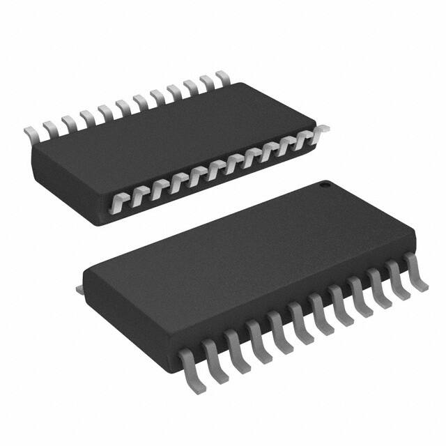
LOW-SIDE SWITCH
DW SUFFIX
EG SUFFIX (PB-FREE)
98ASB42344B
24-PIN SOICW
Features
• Designed to Operate Over Wide Supply Voltages of 5.5 V to 26.5 V
• Interfaces to Microprocessor Using 8-Bit SPI I/O Protocol up to 3.0
MHz
• 1.0 A Peak Current Outputs with Maximum RDS(ON) of 1.6 Ω at TJ 150°C
• Outputs Current-Limited to Accommodate In-Rush Currents
Associated with Switching Incandescent Loads
• Output Voltages Clamped to 53 V During Inductive Switching
• Maximum Sleep Current (IPWR) of 25 μA
• Maximum of 4.0 mA IDD During Operation
• Pb-Free Packaging Designated by Suffix Code EG
ORDERING INFORMATION
Device
MC33291DW/R2
MCZ33291EG/R2
VDD
V PWR
33291
MCU
VPWR
OP 0
SFPD
OP 1
VDD
OP 2
CS
OP 3
SCLK
OP 4
SI
OP 5
SO
OP 6
RESET
OP 7
GND
Figure 1. 33291 Simplified Application Schematic
Freescale Semiconductor, Inc. reserves the right to change the detail specifications, as
may be required, to permit improvements in the design of its products.
© Freescale Semiconductor, Inc., 2008. All rights reserved.
Temperature
Range (TA)
Package
-40°C to 125°C
24 SOICW
ARCHIVE INFORMATION
ARCHIVE INFORMATION
Eight-Output Switch with Serial
Peripheral Interface I/O
�VPWR
21
Output 0
+
VDD
RST
10 μA
25 μA
22
ARCHIVE INFORMATION
+
10 μA
CS
10
Fault Timers
SCLK
3
SI
Bias
53 V
GE
OVD
OT
VDD
SF
RB
OF
SFPD
SFL
CS
SPI
SCLK
Interface
SI
Logic
SO
CSI
CSBI
16
SFPD
15
24
Voltage
Regulator
Gate
Control
To Gates
1–7
1, 2, 11–14, 23
Open
Load
Detect
lLimit
Short
Circuit
Detect
10 μA +
+
-
10 μA
9
RS
Grounds
Overtemperature
Detect
4
SO
Outputs
Serial D/O
Line Driver
5–8, 17–20
From Detectors 1–7
Figure 2. 33291 Simplified Block Diagram
Table 1. Fault Operation
SERIAL OUTPUT (SO) PIN REPORTS
Overvoltage
Overtemperature
Overcurrent
Overvoltage condition reported.
Fault reported by Serial Output (SO) pin.
SO pin reports short to battery/supply or overcurrent condition.
Output ON, Open Load Fault
Not reported.
Output OFF, Open Load Fault
SO pin reports output OFF open load condition.
DEVICE SHUTDOWNS
Overvoltage
Overtemperature
Overcurrent
Total device shutdown at VPWR = 28 V to 36 V. All outputs are latched off while the SPI register is reset
(cleared). Outputs can be turned back on with a new SPI command after VPWR has decayed below 26.5 V.
Only the output experiencing an overtemperature condition turns OFF.
Only the output experiencing an overcurrent shuts down at 1.0 A to 3.0 A after a 70 μs to 250 μs delay, with
SFPD pin grounded. All other outputs will continue to operate in a current limit mode with no shutdown if the
SFPD pin is at 5.0 V (so long as the individual outputs are not experiencing thermal limit conditions).
33291
2
Analog Integrated Circuit Device Data
Freescale Semiconductor
ARCHIVE INFORMATION
Overvoltage
�PIN CONNECTIONS
OP7
1
24
OP0
OP6
2
23
OP1
SCLK
3
22
RST
SI
4
21
VPWR
GND
5
20
GND
GND
6
19
GND
GND
7
18
GND
GND
8
17
GND
SO
9
16
VDD
CS
10
15
SFPD
OP5
11
14
OP2
OP4
12
13
OP3
ARCHIVE INFORMATION
ARCHIVE INFORMATION
PIN CONNECTIONS
Figure 3. 33291 Pin Connections
Table 2. Pin Definitions
Pin
Pin Name
Formal Name
Definition
1
OP7
Output 7
Connection to drain of output MOSFET number seven.
2
OP6
Output 6
Connection to drain of output MOSFET number six.
3
SCLK
System Clock
4
SI
Serial Input
5 – 8, 17 – 20
GND
Ground
9
SO
Serial Output
10
CS
Chip Select
11
OP5
Output 5
Connection to drain of output MOSFET number five.
12
OP4
Output 4
Connection to drain of output MOSFET number four.
13
OP3
Output 3
Connection to drain of output MOSFET number three.
14
OP2
Output 2
Connection to drain of output MOSFET number two.
15
SFPD
Short Fault
Protect Disable
16
VDD
Logic Supply
Plus supply for logic.
21
VPWR
Output MOSFET
Gate Drive Supply
Main power supply.
22
RST
Reset
23
OP1
Output 1
Connection to drain of output MOSFET number one.
24
OP0
Output 0
Connection to drain of output MOSFET number zero.
Clocks the internal Shift registers of the 33291.
This pin is for the input of serial instruction data. SI information is read on the falling
edge of SCLK.
Connection to IC Power Ground and functions as part of heat sinking path.
Tri-stateable output from the Shift register.
Whenever this pin is in a logic low state, data can be transferred from the MCU to the
33291 through the SI pin and from the 33291 to the MCU through the SO pin.
This pin is used to prevent the outputs from latching-OFF because of an overcurrent
condition.
This pin is active low. It is used to clear the SPI Shift register, thereby setting all
output switches OFF.
33291
Analog Integrated Circuit Device Data
Freescale Semiconductor
3
�ELECTRICAL CHARACTERISTICS
MAXIMUM RATINGS
ELECTRICAL CHARACTERISTICS
MAXIMUM RATINGS
Table 3. Maximum Ratings
All voltages are with respect to ground unless otherwise noted. Exceeding these ratings may cause a malfunction or
permanent damage to the device.
Rating
Symbol
Value
VPWR(SUS)
-1.5 to 26.5
VPWR(PK)
-13 to 60
VDD
-0.3 to 7.0
V
VIN
-0.3 to 7.0
V
Power Supply Voltage
ARCHIVE INFORMATION
Transient Conditions (1)
(2)
Input Pin Voltage (3)
Output Clamp Voltage (4)
VOUT(OFF)
5.0 mA ≤ IOUT ≤ 0.5 A
Output Self-Limit Current
Continuous Per Output Current
ESD Voltage
V
45 to 65
(4) (5)
,
IOUT(LIM)
1.0 to 3.0
A
IOUT(CONT)
500
mA
VESD1
±2000
VESD2
±200
ECLAMP
50
mJ
fSPI
3.0
MHz
(6)
V
Human Body Model
(7)
Machine Model (7)
Output Clamp Energy
(8)
Recommended Frequency of SPI Operation
TSTG
-55 to 150
°C
Operating Case Temperature
TC
-40 to 125
°C
Operating Junction Temperature
TJ
-40 to 150
°C
Storage Temperature
Power Dissipation (TA = 25°C) (9)
Peak Package Reflow Temperature During Reflow (10), (11)
PD
2.0
W
TPPRT
Note 11.
°C
Notes
1. Transient capability with external 100 Ω resistor in series with VPWR pin and supply.
2.
3.
4.
5.
Exceeding these limits may cause a malfunction or permanent damage to the device.
Exceeding the limits on SCLK, SI, CS, SFPD, or RST pins may cause permanent damage to the device.
With output OFF.
Continuous output current rating so long as maximum junction temperature is not exceeded. Operation at 125°C ambient temperature
will require maximum output current computation using package RθJA.
6.
7.
ESD data available upon request.
ESD1 testing is performed in accordance with the Human Body Model (CZAP = 200 pF, RZAP = 1500 Ω), ESD2 testing is performed in
accordance with the Machine Model (CZAP = 200pF, RZAP = 0 Ω).
8.
9.
10.
Maximum output clamp energy capability at 150°C junction temperature using a single non-repetitive pulse method.
Maximum power dissipation at indicated junction temperature with no heat sink used.
Pin soldering temperature limit is for 10 seconds maximum duration. Not designed for immersion soldering. Exceeding these limits may
cause malfunction or permanent damage to the device.
Freescale’s Package Reflow capability meets Pb-free requirements for JEDEC standard J-STD-020C. For Peak Package Reflow
Temperature and Moisture Sensitivity Levels (MSL),
Go to www.freescale.com, search by part number [e.g. remove prefixes/suffixes and enter the core ID to view all orderable parts. (i.e.
MC33xxxD enter 33xxx), and review parametrics.
11.
33291
4
Analog Integrated Circuit Device Data
Freescale Semiconductor
ARCHIVE INFORMATION
V
Normal Operation (Steady-State)
Logic Supply Voltage
Unit
�ELECTRICAL CHARACTERISTICS
MAXIMUM RATINGS
Table 3. Maximum Ratings (continued)
All voltages are with respect to ground unless otherwise noted. Exceeding these ratings may cause a malfunction or
permanent damage to the device.
Rating
Symbol
Value
Junction-to-Ambient (Natural Convection, Single-Layer Board) (12), (13)
RθJA
RθJMA
68
°C/W
Thermal Resistance
Junction-to-Ambient (Natural Convection, Four-Layer Board) (12), (14)
RθJL
44
20
Notes
12. Junction temperature is a function of die size, on-chip power dissipation, package thermal resistance, mounting site (board)
temperature, ambient temperature, air flow, power dissipation of other components on the board, and board thermal resistance.
13. Per SEMI G38-87 and JEDEC JESD51-2 with the single layer board (JESD51-3) horizontal.
14. Per JEDEC JESD51-6 with the board (JESD51-7) horizontal.
15. Thermal resistance between the die and the printed circuit board per JEDEC JESD51-8.
ARCHIVE INFORMATION
ARCHIVE INFORMATION
Junction to Board (15)
Unit
33291
Analog Integrated Circuit Device Data
Freescale Semiconductor
5
�ELECTRICAL CHARACTERISTICS
STATIC ELECTRICAL CHARACTERISTICS
STATIC ELECTRICAL CHARACTERISTICS
Table 4. Static Electrical Characteristics
Characteristics noted under conditions 4.5 V ≤ VDD ≤ 5.5 V, 9.0 V ≤ VPWR ≤ 16 V, -40°C ≤ TA ≤ 125°C, unless otherwise noted.
Typical values noted reflect the approximate value with VBAT = 13 V, TA = 25°C.
Characteristic
Symbol
Min
Typ
Max
Unit
Quasi-Functional (16)
VPWR(QF)
5.5
–
9.0
Fully Operational
VPWR(FO)
9.0
–
26.5
Supply Current (All Outputs ON, IOUT = 0.5 A)
VPWR(ON)
–
1.0
2.0
mA
Sleep State Supply Current at RST ≤ 0.2 VDD and/or VDD < 0.5 V
IPWR(ON)
–
1.0
2.5
μA
Sleep State Output Leakage Current (Per Output, RST = 0 V)
IPWR(SS)
–
1.0
2.5
μA
VOV
28
32
36
V
POWER INPUT
V
Overvoltage Shutdown
Overvoltage Shutdown Hysteresis (17)
VOV(HYS)
0.2
0.8
1.5
V
Logic Supply Voltage
VDD
4.5
–
5.5
V
Logic Supply Current (18)
IDD
RST ≥ 0.7 VDD
–
1.0
4.0
mA
RST ≤ 0.5 V
–
–
25
μA
2.5
–
3.5
V
Logic Supply Undervoltage Lockout Threshold
(19)
VDD(UVLO)
POWER OUTPUT
Drain-to-Source ON Resistance (IOUT = 0.5 A, TJ - 25°C)
Ω
RDS(ON)
VPWR = 5.5 V
–
–
2.0
VPWR = 9.0 V
–
0.6
1.2
VPWR = 13 V
–
0.55
1.0
VPWR = 5.5 V
–
–
3.0
VPWR = 9.0 V
–
1.2
1.6
VPWR = 13 V
–
1.0
1.2
1.0
2.0
3.0
Drain-to-Source ON Resistance (IOUT = 0.5 A, TJ - 150°C)
Output Self-Limiting Current
IOUT(LIM)
Outputs Programmed ON, VOUT = 0.6 VDD
Output Fault Detect Threshold (20)
Output Programmed OFF
Ω
RDS(ON)
A
V
VOUTth(F)
2.5
3.0
3.5
Notes
16. SPI inputs and outputs operational. Fault status reporting may not be fully operational within this voltage range. Outputs remain
operational somewhat below this VPWR range, but RDS(ON) will increase, causing power dissipation to increase. Outputs will reestablish their instructed state following a VPWR interruption as long as VDD remains non-interrupted.
17.
18.
19.
20.
This parameter is guaranteed by design, but it is not production tested.
Measured with the RST pin held at a logic high state. Outputs can be OFF or ON or in any combination thereof.
Device incorporates a power-ON reset function. For VDD less than the Undervoltage Lockout Threshold voltage, all data registers are
reset and all outputs are disabled.
Output Fault Detect Threshold with outputs programmed OFF. Output fault detect thresholds are the same for output opens and shorts.
33291
6
Analog Integrated Circuit Device Data
Freescale Semiconductor
ARCHIVE INFORMATION
ARCHIVE INFORMATION
Supply Voltage Range
�ELECTRICAL CHARACTERISTICS
STATIC ELECTRICAL CHARACTERISTICS
Table 4. Static Electrical Characteristics (continued)
Characteristics noted under conditions 4.5 V ≤ VDD ≤ 5.5 V, 9.0 V ≤ VPWR ≤ 16 V, -40°C ≤ TA ≤ 125°C, unless otherwise noted.
Typical values noted reflect the approximate value with VBAT = 13 V, TA = 25°C.
Symbol
Output OFF Open Load Detect Current (21)
Typ
Max
30
50
100
Output Clamp Voltage
V
VOK
2.0 mA < IOUT < 200 mA
Unit
μA
IOCO
Output Programmed OFF, VOUT = 0.6 VDD
45
53
65
IOUT(LKG)
-25
0
25
μA
TLIM
155
180
–
°C
TLIM(HYS)
–
10
20
°C
V IH
0.7
–
1.0
VDD
V IL
0
–
0.2
VDD
VI (HYS)
50
100
500
mV
SI Pull-Up Current (SI = 0 V)
ISI
0
10
20
μA
CS Pull-Up Current (CS = 0 V)
ICS
0
10
20
μA
SCLK Pull-Down Current (SCLK = 5.0 V)
ISCLK
0
10
20
μA
RST Pull-Down Current (RST = 5.0 V)
I RST
5.0
25
50
μA
SFPD Pull-Down Current (SFPD = 5.0 V)
ISFPD
5.0
10
25
μA
SO High-State Output Voltage (IOH = 1.0 mA)
VSOH
–
V
SO Low-State Output Voltage (IOL = -1.6 mA)
VSOL
–
0.2
0.4
V
SO Tri-State Leakage Current (CS = 0.7 VDD, 0 V < VSO < VDD)
ISOT
-10
0
10
μA
CIN
–
–
12
pF
CSOT
–
–
20
pF
Output Leakage Current (VDD < 2.0 V)
(22)
Overtemperature Shutdown (Outputs OFF)
ARCHIVE INFORMATION
Min
Overtemperature Shutdown Hysteresis
(23)
(23)
DIGITAL INTERFACE
Input Logic High Voltage (24)
Input Logic Low Voltage
(24)
Input Logic Threshold Hysteresis (SCLK, RST, and SFPD)
Input Capacitance (0 V < VDD < 5.5 V)
(26)
SO Tn-State Capacitance (0 V < VDD < 5.5 V)
(27)
(25)
VDD - 0.4 V VDD - 0.2 V
Notes
21. Output OFF Open Load Detect Current is the current required to flow through the load for the purpose of detecting the existence of an
open load condition when the specific output is commanded to be OFF.
22. Output leakage current measured with the output OFF and at 16 V.
23. This parameter is guaranteed by design, but it is not production tested.
24. Upper and lower logic threshold voltage levels apply to SI, CS, SCLK, RST, and SFPD inputs.
25. Hysteresis is characterized, but it is not production tested.
26. Input capacitance of SI CS, SCLK, RST, and SFPD for 0 V < VDD < 5.5 V. This parameter is guaranteed by design, but it is not production
tested.
27. Tri-state capacitance of SO for 0 V < VDD < 5.5 V. This parameter is guaranteed by design, but it is not production tested.
33291
Analog Integrated Circuit Device Data
Freescale Semiconductor
7
ARCHIVE INFORMATION
Characteristic
�ELECTRICAL CHARACTERISTICS
DYNAMIC ELECTRICAL CHARACTERISTICS
DYNAMIC ELECTRICAL CHARACTERISTICS
Table 5. Dynamic Electrical Characteristics
Characteristics noted under conditions 4.5 V ≤ VDD ≤ 5.5 V, 9.0 V ≤ VPWR ≤ 16 V, -40°C ≤ TA ≤ 125°C, unless otherwise noted.
Typical values noted reflect the approximate parameter mean at TA = 25°C under nominal conditions, unless otherwise noted.
Characteristic
Symbol
Min
Typ
Max
Unit
tR
0.4
5.0
20
μs
tF
0.4
5.0
20
μs
tDLY (ON)
1.0
15
50
μs
tDLY (OFF)
1.0
15
50
μs
Output Rise Time (VPWR = 13 V, RL = 26 Ω) (28)
Output Fall Time (VPWR = 13 V, RL = 26 Ω)
(28)
ARCHIVE INFORMATION
Output Turn-ON Delay Time (VPWR = 13 V, RL = 26 Ω)
(29)
Output Turn-OFF Delay Time (VPWR = 13 V, RL = 26 Ω)
Output Short Fault Disable Report Delay
(30)
(31)
μs
tDLY (SF)
SFPD = 0.2 x VDD
70
150
250
70
150
250
tW(RST)
–
50
167
ns
Falling Edge of CS to Rising Edge of SCLK (Required Setup Time)
tLEAD
–
50
167
ns
Falling Edge of SCLK to Rising Edge of CS (Required for Setup Time)
tLAG
–
50
167
ns
SI to Falling Edge of SCLK (Required for Setup Time)
tSI (SU)
–
25
83
ns
Falling Edge of SCLK to SI (Required for Hold Time)
tSI (HOLD)
–
25
83
ns
tR (SO)
–
25
50
ns
tF (SO)
–
25
50
ns
tR (SI)
–
–
50
ns
Output OFF Fault Report Delay
(32)
μs
tDLY (OFF)
SFPD = 0.2 x VDD
DIGITAL INTERFACE TIMING
Required Low State Duration for RST (VIL < 0.2 VDD) (33)
SO Rise Time (CL = 200 pF)
SO Fall Time (CL = 200 pF)
SI, CS, SCLK, Incoming Signal Rise Time
SI, CS, SCLK, Incoming Signal Fall Time
(34)
(34)
tF (SI)
–
–
50
ns
Time from Falling Edge of CS to SO Low Impedance
(35)
tSO(EN)
–
–
110
ns
Time from Rising Edge of CS to SO High Impedance
(36)
tSO(DIS)
–
–
110
ns
–
65
105
Time from Rising Edge of SCLK to SO Data Valid
0.2 VDD ≤ SO ≥ 0.8 VDD, CL = 200 pF
(37)
tVALID
ns
Notes
28. Output Rise and Fall time respectively measured across a 26 Ω resistive load at 10% to 90% and 90% to 10% voltage points.
29. Output Turn-ON Delay time measured from 50% rising edge of CS to 90% of Output OFF voltage (VPWR) with RL = 26 Ω resistive load.
30.
Output Turn-OFF Delay time measured from 50% rising edge of CS to 10% of Output OFF voltage (VPWR) with RL = 26 Ω resistive load.
31.
Propagation time of Short Fault Disable Report measured from 50% rising edge of CS to 10% Output OFF voltage (VPWR), VPWR =
6.0 V and SFPD = 0.2 x VDD.
32.
Output OFF Fault Report Delay measured from 50% rising edge of CS to 10% rising edge of Output OFF voltage (VPWR).
33.
34.
35.
36.
37.
RST Low duration measured with outputs enabled and going to OFF or disabled condition.
Rise and Fall time of incoming SI, CS, and SCLK signals suggested for design consideration to prevent the occurrence of double pulsing.
Time required for output status data to be available for use at the SO pin.
Time required for output status data to be terminated at the SO pin.
Time required to obtain valid data out from SO following the rise of SCLK. See Figure 7, page 10.
33291
8
Analog Integrated Circuit Device Data
Freescale Semiconductor
ARCHIVE INFORMATION
POWER OUTPUT TIMING
�ELECTRICAL CHARACTERISTICS
TIMING DIAGRAM
TIMING DIAGRAM
VIH
RST
0.2 VDD
VIL
tW(RST)
VIH
0.2 VDD
VIL
ARCHIVE INFORMATION
tLEAD
tW(SCLKH
tR
)
tLAG
VIH
0.7 VDD
SCLK
0.2 VDD
VIL
tW(SCLKL)
tSI(HOLD)
tSI(SU)
0.7 VDD
SI
tF
VIH
Don't Care
Valid
Don't Care
Valid
Don't Care
VIL
0.2 VDD
Figure 4. Input Timing Switch Characteristics
ELECTRICAL PERFORMANCE CURVES
VDD = 5.0 V
VDD = 5.0 V
VPull-Up = 2.5 V
RL = 1.0 kΩ
33291
SCLK
SO
Under
Test
CL = 200 pF
CL represents the total capacitance of the test fixture and probe.
Figure 5. Valid Data Delay Time and
Valid Time Test Circuit
CS
33291
Under
Test
SO
CL = 20 pF
CL represents the total capacitance of the test fixture and probe.
Figure 6. Enable and Disable Time Test Circuit
33291
Analog Integrated Circuit Device Data
Freescale Semiconductor
9
ARCHIVE INFORMATION
CS
�ELECTRICAL CHARACTERISTICS
ELECTRICAL PERFORMANCE CURVES
tR (SI)
tF (SI)
< 50 ns
< 50 ns
0.2 VDD
(High-to-Low)
RL = 26 Ω
VOH
0.7 VDD
33291
CS
0.2 VDD
SO
ARCHIVE INFORMATION
0
VOL
tR (SO)
tVALID
CL
tF (SO)
VOH
0.7 VDD
0.2 VDD
tDLY(HL)
Output
Under
Test
VOL
SO (Low-to-High) is for an output with internal conditions such that
the low-to-high transition of CS causes the SO output to switch from
high to low.
CL represents the total capacitance of the test fixture and probe.
Figure 9. Switching Time Test Circuit
Figure 7. Valid Data Delay Time and
Valid Time Waveforms
tR(SI)
< 50 ns
CS
0.2 VDD
VDD = 5.0 V
tF(SI)
< 50 ns
90%
10%
(High-to-Low)
5.0 V
0.7 VDD
CS
tSO(DIS)
VTri-State
tSO(EN)
Output
tSO(DIS)
tSO(DIS)
VOH
90%
CL represents the total capacitance of the test fixture and probe.
10%
(Low-to-High)
Under
Test
ΙL = 2.0 Α
(Ουτπυτ ΟΝ)
CL = 20 pF
90%
10%
SO
33291
0
tSO(EN)
SO
VPWR = 11 V
VTri-State
1. SO (high-to-low) waveform is for SO output with internal conditions such
that SO output is low except when an output is disabled as a result of detecting a circuit fault with CS in a High Logic state; e.g., open load.
2. SO (low-to-high) waveform is for SO output with internal conditions such
that SO output is high except when an output is disabled as a result of detecting a circuit fault with CS in a High Logic state; e.g., shortened load.
Figure 10. Output Fault Unlatch Disable
Delay Test Circuit
Figure 8. Enable and Disable Time Waveforms
33291
10
Analog Integrated Circuit Device Data
Freescale Semiconductor
ARCHIVE INFORMATION
tDLY(LH)
(Low-to-High)
VPWR = 14 V
50%
SCLK
SO
VDD = 5.0 V
5.0 V
0.7 VDD
�ELECTRICAL CHARACTERISTICS
ELECTRICAL PERFORMANCE CURVES
tF(SI)
< 50 ns
tR(SI)
< 50 ns
5.0 V
90%
50%
CS
10%
10%
90%
VOL
ARCHIVE INFORMATION
tDLY(ON)
1. tDLY(ON) and tDLY(OFF) are turn-ON and turn-OFF propagation delay
times.
2. Turn-OFF is an output programmed from an ON to an OFF state.
3. Turn-ON is an output programmed from and OFF to an ON state.
Figure 11. Turn-On/-Off Waveforms
Output Voltage
Waveform
VOL
14 V
Output Voltage
Waveform 2
50%
< 50 ns
5.0 V
90%
10%
0
0
14 V
Output Voltage
Waveform 1
< 50 ns
CS
tDLY(OFF)
tF(SI)
VOFF = 11 V
50%
tPDLY(OFF)
Output Current
Waveform
VON = 5.0 V
IO(CL)
50%
0
1. tPDLY(OFF) is the output fault unlatch disable propagation delay time required to correctly report an output fault after CS rises. It represents an
output commanded ON while having an existing output short (overcurrent)
to supply.
2. The SFPD pin < 0.2 V.
Figure 12. Output Fault Unlatch Disable
Delay Waveforms
33291
Analog Integrated Circuit Device Data
Freescale Semiconductor
11
ARCHIVE INFORMATION
tR(SI)
�FUNCTIONAL DESCRIPTION
INTRODUCTION
FUNCTIONAL DESCRIPTION
The 33291 was conceived, specified, designed, and
developed for automotive applications. It is an eight-output
low-side power switch having 8-bit serial control. The 33291
incorporates SMARTMOS technology having CMOS logic,
bipolar/MOS analog circuitry, and independent state of the
art double diffused MOS (DMOS) power output transistors.
Many benefits are realized as a direct result of using this
mixed technology. A simplified block diagram delineates
33291 in Figure 2.
Where bipolar devices require considerable control
current for their operation, structured MOS devices, since
they are voltage controlled, require only transient gate
charging current affording a significant decrease in power
consumption. The CMOS capability of the SMARTMOS
process allows significant amounts of logic to be
economically incorporated into the monolithic design.
Additionally, the bipolar/MOS analog circuits embedded
within the updrain power DMOS output transistors monitor
and provide fast, independent protection control functions for
each individual output. All outputs have internal 45 V at 0.5 A
independent output voltage clamps to provide fast inductive
turn-off and transient protection.
The 33291 uses high-efficiency updrain power DMOS
output transistors exhibiting very low room temperature
drain-to-source ON resistance values (RDS(ON) ≤ 1.0 Ω at
13 V VPWR) and dense CMOS control logic. Operational bias
currents of less than 2.0 mA (1.0 mA typical) with any
combination of outputs ON are the result of using this mixed
technology and would not be possible with bipolar structures.
To accomplish a comparable functional feature set using a
bipolar structure approach would result in a device requiring
hundreds of milliamperes of internal bias and control current.
This would represent a very large amount of power to be
consumed by the device itself and not available for load use.
During operation, the 33291 functions as an eight output
serial switch serving as a microcontroller (MCU) bus
expander and buffer with fault management and fault
reporting features. In doing so, the device directly relieves the
MCU of the fault management functions. The 33291 directly
relieves the MCU of the fault management functions. The
33291 directly interfaces to an MCU, operating at system
clock serial frequencies in excess of 3.0 MHz. It uses a
Synchronous Peripheral Interface (SPI) for control and
diagnostic readout. Figure 13 illustrates the basic SPI
configuration between an MCU and one 33291.
MC68HCXX
Microcontroller
Shift Register
Receive
Buffer
Parallel
Ports
33291
MOSI
SI
MISO
SO
SCLK
Shift Register
To
Logic
RST
CS
Figure 13. SPI Interface with Microcontroller
The circuit can also be used in a variety of other
applications in the computer, telecommunications, and
industrial fields. It is parametrically specified over an input
battery/supply range of 9.0 V to 16 V but is designed to
operate over a considerably wider range of 5.5 V to 26.5 V.
The design incorporates the use of logic level MOSFETs as
output devices. These MOSFETs are sufficiently turned ON
with a gate voltage of less than 5.0 V, thus eliminating the
need for an internal charge pump. Each output is identically
sized and independent in operation. The efficiency of each
output transistor is such that at room temperature with as little
as 9.0 V supply (VPWR), the maximum RDS(ON) of an output
at room temperature is 1.2 Ω (0.9 Ω typical) and increases to
only 2.0 Ω as VPWR is decreased to 5.5 V.
All inputs are compatible with 5.0 V CMOS logic levels,
incorporating negative or inverted logic. Whenever an input is
programmed to a logic low state (3.0 V), the output being
controlled will be high and turned OFF.
One main advantage of the 33291 is the serial port. When
coupled to an MCU, it receives ON/OFF commands from the
MCU and in return transmits the drain status of the device’s
output switches. Many devices can be daisy-chained
together, forming a larger system, as illustrated in Figure 14,
page 13.
Note In this example, only one dedicated MCU parallel
port (aside from the required SPI) is required for chip select
to control 32 possible loads.
33291
12
Analog Integrated Circuit Device Data
Freescale Semiconductor
ARCHIVE INFORMATION
ARCHIVE INFORMATION
INTRODUCTION
�FUNCTIONAL DESCRIPTION
INTRODUCTION
SCLK
Parallel Port
SCLK
CS
SCLK
CS
SCLK
CS
SCLK
SO
SI
SO
SI
SO
SI
SO
SI
IRQ
ARCHIVE INFORMATION
MOSI
33291
8 Outputs
33291
33291
33291
8 Outputs
8 Outputs
8 Outputs
Figure 14. 33291 SPI System Daisy Chain
Multiple 33291 devices can also be controlled in a parallel
however, not at the same time. Only when the master is not
input fashion using SPI, illustrated in Figure 15. This figure
communicating can a slave assume the mastership and
shows a possible 24 loads being controlled by only three
communicate. MCU master control is switched through the
dedicated parallel MCU ports used for chip select.
use of the slave select (SS) pin of the MCUs. A master will
become a slave when it detects a logic low state on its SS pin.
These basic examples make the 33291 very attractive for
applications
where a large number of loads require efficient
33291
control.
To
this
end, the popular Synchronous Serial
MOSI
SI
8 Outputs
Peripheral Interface (SPI) protocol is incorporated to
SCLK
SCLK
communicate efficiently with the MCU.
MC68XX
Microcontroller
SPI
CS
SPI SYSTEM ATTRIBUTES
33291
8 Outputs
SI
Parallel
Ports
A0
A1
A2
SCLK
CS
33291
SI
8 Outputs
SCLK
CS
Figure 15. Parallel Input SPI Control
Figure 16, page 14, illustrates a basic method of
controlling multiple 33291 devices using two MCUs. A system
can have only one master MCU at any given instant of time
and one or more slave MCUs. Master control of the system
must pass from one MCU to the other in an orderly manner.
The master MCU supplies the system clock signal (top MCU
designated the master); the lower MCU being the slave. It is
possible to have a system with more than one master;
The SPI system is flexible enough to communicate directly
with numerous standard peripherals and MCUs available
from Motorola and other semiconductor manufacturers. SPI
reduces the number of pins necessary for input/output (I/O)
on the 33291. It also offers an easy means of expanding the
I/O function using few MCU pins. The SPI system of
communication consists of the MCU transmitting, in return it
receives one data-bit of information per system clock cycle.
Data bits of information are simultaneously transmitted by
one pin, Master Out Serial In (MOSI), and received by
another pin, Master In Serial Out (MISO), of the MCU.
Some features of SPI are as follows:
• Full duplex, three-wire synchronous data transfer
• Each microcontroller can be a master or a slave
• Provides write collision flag protection
• Provides end of message interrupt flag
• Four I/Os associated with SPI (MOSI, MISO, SCLK, SS)
• Drawbacks to SPI are as follows:
• An MCU is required for efficient operational control
• In contrast to parallel input control it is slower at performing
pulse width modulating (PWM) functions.
33291
Analog Integrated Circuit Device Data
Freescale Semiconductor
13
ARCHIVE INFORMATION
MC68XX
Microcontroller
SPI
CS
MISO
�FUNCTIONAL DESCRIPTION
INTRODUCTION
MC68XX
Microcontroller
SPI
(Master)
B0
A0
A1
B1 Parallel
Ports
A2
33291
CS
SCLK
8 Outputs
8-Bit
SO
8-Bit
SCLK
MISO
SI
MOSI
VDD
33291
SS
CS
SCLK
(Alternate Master)
B0 Parallel A0
B1 Ports A1
A2
SCLK
8-Bit
VDD
8 Outputs
8-Bit
SO
SI
33291
CS
SCLK
8 Outputs
8-Bit
MISO
SO
MOSI
SI
SS
Figure 16. Multiple MCU SPI Control
33291
14
Analog Integrated Circuit Device Data
Freescale Semiconductor
ARCHIVE INFORMATION
ARCHIVE INFORMATION
MC68XX
Microcontroller
SPI
�FUNCTIONAL DESCRIPTION
FUNCTIONAL PIN DESCRIPTION
FUNCTIONAL PIN DESCRIPTION
The 33291 receives its MCU communication through the
ARCHIVE INFORMATION
CS pin. Whenever this pin is in a logic low state, data can be
transferred from the MCU to the 33291 by way of the SI pin
and from the 33291 to the MCU through the SO pin. Clockedin data from the MCU is transferred from the 33291 Shift
register and latched into the power outputs on the rising edge
of the CS signal. On the falling edge of the CS signal, drain
status information is transferred from the power outputs then
loaded into the Shift register of the device. The CS pin also
controls the output driver of the serial output (SO) pin.
Whenever the CS pin goes to a logic low state, the SO pin
output driver is enabled allowing information to be transferred
from the 33291 to the MCU. To avoid data corruption or the
generation of spurious data, it is essential the high-to-low
transition of the CS signal occur only when SCLK is in a logic
low state.
SYSTEM CLOCK (SCLK)
The system clock (SCLK) pin clocks the internal shift
registers of the 33291. The serial input (SI) pin accepts data
into the Input Shift register on the falling edge of the SCLK
signal while the serial output (SO) pin shifts data information
out of the SO line driver on the rising edge of the SCLK signal.
False clocking of the Shift register must be avoided to
guarantee validity of data. It is essential the SCLK pin be in a
logic low state whenever the chip select bar (CS) pin makes
any transition. For this reason, it is recommended, though not
absolutely necessary, the SCLK pin be kept in a low logic
state as long as the device is not accessed (CS in logic high
state). When CS is in a logic high state, signals at the SCLK
and SI pins are ignored and SO is tri-stated (high
impedance). See the Data Transfer Timing diagram in
Figure 18, page 17.
SERIAL INSTRUCTION (SI)
This pin is for the input of serial instruction (SI) data. SI is
read on the falling edge of SCLK. A logic high state present
on this pin when the SCLK signal rises will program a specific
output OFF. In turn, CS pin turns OFF the specific output on
the rising edge of the CS signal. Conversely, a logic low state
present on the SI pin will program the output ON, In turn, the
pin turns ON the specific output on the rising edge of the CS
signal.
To program the eight outputs of the 33291 ON or OFF, an
8-bit serial stream of data is required to be synchronously
entered into the SI pin starting with Output 7, followed by
Output 6, Output 5, and so on, to Output 0. Referring to
Figure 18, the DO bit is the most significant bit (MSB)
corresponding to Output 7. For each rise of the SCLK signal,
with CS held in a logic low state, a data-bit instruction (ON or
OFF) is synchronously loaded into the Shift register per the
data-bit SI state. The Shift register is full after eight bits of
information have been entered. To preserve data integrity,
care should be taken to not transition SI as SCLK transitions
from a low-to-high logic state.
SERIAL OUTPUT (SO)
The serial output (SO) pin is the tri-stateable output from
the Shift register. The SO pin remains in a high impedance
state until the CS pin goes to a logic low state. The SO data
reports the drain status, either high or low relative to the
previous command word. The SO pin changes state on the
rising edge of SCLK and reads out on the falling edge of
SCLK. When an output is OFF and not faulted, the
corresponding SO data-bit is a high state. When an output is
ON, and there is no fault, the corresponding data-bit on the
SO pin will be a low logic state. The SI/SO shifting of data
follows a first-in-first-out (FIFO) protocol with both input and
output words transferring the MSB first. Referring to
Figure 18, the DO bit is the MSB corresponding to Output 7
relative to the previous command word. The SO pin is not
affected by the status of the RST pin.
RESET (RST)
The 33291 Reset (RST) pin is active low. It is used to clear
the SPI Shift register. In doing so, all output switches are set
at OFF. With the device in a system with an MCU, upon initial
system power-up, the MCU holds the RST pin of the device
in a logic low state, ensuring all outputs to be OFF until both
the VDD and VPWR pin voltages are adequate for predictable
operation. After the 33291 is reset, the MCU is ready to
assert system control with all output switches initially OFF.
If the VPWR pin of the 33291 experiences a low voltage,
following normal operation, the MCU should pull the RST pin
low to shut down the outputs and clear the input data register.
The RST pin is active low and has an internal pull-down
incorporated to ensure operational predictability should the
external pull-down of the MCU open circuit. The internal pulldown is only 25 μA, affording safe and easy interfacing to the
MCU. The RST pin of the 33291 should be pulled to a logic
low state for a duration of at least 250 ns to ensure reliable a
reset.
A simple power ON reset delay of the system can be
programmed through the use of an RC network comprised of
a shunt capacitor from the RST pin to Ground and a resistor
to VDD, illustrated in Figure 17. Care should be exercised
ensuring proper discharge of the capacitor. Careful attention
eliminates adverse delay of the RST and damage of the MCU
if it pulls the Reset line low, thereby accomplishing
initialization for turn ON delay. It may be easier to incorporate
delay into the software program and use a parallel port pin of
the MCU to control the 33291 RST pin.
33291
Analog Integrated Circuit Device Data
Freescale Semiconductor
15
ARCHIVE INFORMATION
CHIP SELECT (CS)
�FUNCTIONAL DESCRIPTION
FUNCTIONAL PIN DESCRIPTION
+
RDLY
20 μA
Reset
MCU
Reset
CDLY
33291
Figure 17. Power ON Reset
ARCHIVE INFORMATION
SHORT FAULT PROTECT DISABLE (SFPD)
The Short Fault Protect Disable (SFPD) pin is used to
prevent the outputs from latching-off due to an overcurrent
condition. This feature provides control of incandescent lamp
loads where in-rush currents exceed the device’s analog
current limits. Essentially the SFPD pin determines whether
the 33291 output(s) will instantly shut down upon sensing an
output short or remain ON in a current limiting mode of
operation until the output short is removed or thermal
shutdown is reached. If the SFPD pin is tied to VDD = 5.0 V
the 33291 output(s) will remain ON in a current limited mode
of operation upon encountering a load short to supply or
overcurrent condition. When the SFPD pin is grounded, a
short circuit will immediately shut down only the output
affected. Other outputs not having a fault condition will
operate normally. The short circuit operation is addressed in
more detail later.
POWER CONSUMPTION
The 33291 has extremely low power consumption in both
the operating and standby modes. In the standby, or Sleep,
mode, with VDD ≤ 2.0 V, the current consumed by the VPWR
pin is less than 25 μA. In the operating mode, the current
drawn by the VDD pin is less than 4.0 mA (1.0 mA typical)
while the current drawn at the VPWR pin is 2.0 mA maximum
PARALLELING OF OUTPUTS
Using MOSFETs as output switches permits connecting
any combination of outputs together. RDS(ON) of MOSFETs
have an inherent positive temperature coefficient providing
balanced current sharing between outputs without
destructive operation (bipolar outputs could not be paralleled
in this fashion as thermal run-away would likely occur). The
device can even be operated with all outputs tied together.
This mode of operation may be desirable in the event the
application requires lower power dissipation or the added
capability of switching higher currents.
Performance of parallel operation results in a
corresponding decrease in RDS(ON) while the Output OFF
Open Load Detect Currents and the Output Current Limits
increase correspondingly (by a factor of eight if all outputs are
paralleled). Less than 125 mΩ RDS(ON) at 25°C with current
limiting of 8 A to 24 A will result if all outputs are paralleled
together. There will be no change in the overvoltage detect or
the OFF output threshold voltage range. The advantage of
paralleling outputs within the same 33291 affords the
existence of minimal RDS(ON) and output clamp voltage
variation between outputs.
Typically, the variation of RDS(ON) between outputs of the
same device is less than 0.5 percent. The variation in clamp
voltages, potentially affecting dynamic current sharing, is less
than five percent. Paralleling outputs from two or more
different devices is possible, but it is not recommended.
There is no guarantee the RDS(ON) and clamp voltage of the
two devices will match. System level thermal design analysis
and verification should be conducted whenever paralleling
outputs, particularly where different devices are involved.
33291
16
Analog Integrated Circuit Device Data
Freescale Semiconductor
ARCHIVE INFORMATION
VDD
(1.0 mA typical). During normal operation, turning outputs
ON increases IPWR by only 20 μA per output. Each output
experiencing a soft short (overcurrent conditions just under
the current limit) adds 0.5 mA to the IPWR current
�Analog Integrated Circuit Device Data
Freescale Semiconductor
OD*
D0
OD*
D1
OD*
D2
OD*
D4
Old Data
Old Data
OD*
D3
OD*
D5
OD*
D6
OD*
D7
D0*
D8
D1*
D9
D3*
D11
New Data DO0
New Data DO7
D2*
D10
D4*
D12
D5*
D13
D6*
D14
D7*
D15
Data from the Shift Register is transferred to the Output Power Switches.
Will change state on the rising edge of the SCLK pin signal.
Will accept data on the falling edge of the SCLK pin signal.
CS Low-to-High
SO
SI
ARCHIVE INFORMATION
SO pin is enabled. Output Status information transferred to Output Shift Register.
CS High-to-Low
Data Transfer Timing (General)
NOTES: 1.RST pin is in a logic high-state during the above operation.
2.D0, D1, D2, ..., and D15 relate to the ordered entry of program data into the MC33291 with D0/D8 bits (MSB) corresponding to Output 7 and D7/D15 corresponding to Output 0.
3.D0*, D1*, D2*, ..., and D7* relate to the ordered data out of the MC33291 with D0* bit (MSB) corresponding to Output 7.
4.OD* corresponds to Old Databits.
5.For brevity, only DO7 and DO0 are shown which respectively correspond to Output 7 and Output 0.
Output 0
Output 7
SO
SI
SCLK
CS
ARCHIVE INFORMATION
FUNCTIONAL DESCRIPTION
Figure 18. Data Transfer Timing
33291
17
�FUNCTIONAL DESCRIPTION
ARCHIVE INFORMATION
INTRODUCTION
The MCU can perform a parity check of the fault logic
operation by comparing the command 8-bit word to the status
8-bit word. Assume after system reset, the MCU first sends
an 8-bit command word to the 33291. This word is called
Command Word 1. Each output to be turned ON will have its
corresponding data bit low. Refer to the data transfer timing
illustration in Figure 18.
As Command Word 1 is being written into the Shift register
of the 33291, a status word is being simultaneously written
and received by the MCU. However, the word being received
by the MCU is the status of the previous write word to the
33291, Status Word 0. If the command word of the MCU is
written a second time (Command Word 2 = Command Word
1), the word received by the MCU, Status Word 2, is the
status of Command Word 1. The timing diagram illustrated in
Figure 18 depicts this operation. Status Word 2 is then
compared with Command Word 1. The MCU will Exclusive
OR Status Word 2 with Command Word 1 to determine if the
two words are identical. If the two words are identical, no
faults exist. The timing between the two write words must be
greater than 100 μs to receive proper drain status. The
system data bus integrity may be tested by writing two like
words to the 33291 within a few microseconds of each other.
INITIAL SYSTEM SETUP TIMING
The MCU can monitor two kinds of faults:
1. Communication errors on the data bus
2. Actual faults of the output loads
After initial system startup or reset, the MCU will write one
word to the 33291. If the word is repeated within
approximately five microseconds of the first word, the word
received by the MCU, at the end of the repeated word, serves
as a confirmation of data bus integrity (1). At startup, the
33291 will take 25 μs to 100 μs before a repeat of the first
word should be repeated at least 100 μs later to verify the
status of the outputs.
The SO of the 33291 will indicate any one of four faults.
The four possible faults are:
output. The shutdown following an Overtemperature
condition is independent of the system clock or any other
logic signal. Each independent output shuts down at 155°C
to 185°C. When an output shuts down due to an
Overtemperature Fault, no other outputs are affected. The
MCU recognizes the fault since the output was commanded
to be ON and the status word indicates it is OFF. A maximum
hysteresis of 20°C ensures an adequate time delay between
output turn OFF and recovery. This avoids a very rapid turn
ON and turn OFF of the device around the Overtemperature
threshold. When the temperature falls below the recovery
level for the Overtemperature Fault, the device will turn ON
only if the Command Word during the next write cycle
indicates the output should be turned ON.
OVERVOLTAGE FAULT
An Overvoltage condition on the VPWR pin causes the
33291 to shut down all outputs until the overvoltage condition
is removed and the device is re-programmed by the SPI. The
overvoltage threshold on the VPWR pin is specified as 28 V
to 36 V with 1.0 V typical hysteresis. Following the
overvoltage condition, the next write cycle sends the SO pin
the hexadecimal word $FF (all ones), indicating all outputs
are turned OFF. In this way, potentially dangerous timing
problems are avoided and the MCU reset routine ensures an
orderly startup of the loads. The 33291 does not detect an
overvoltage on the VDD pin. Other external circuitry, such as
the Freescale 33161 Universal Voltage Monitor, is necessary
to accomplish this function.
OUTPUT OFF OPEN LOAD FAULT
An Output OFF Open Load Fault is the detection and
reporting of an open load when the corresponding output is
disabled (input bit programmed to a logic high state). To
understand the operation of the Open Load Fault detect
circuit, see Figure 19. The Output OFF Open Load Fault is
detected by comparing the drain voltage of the specific
MOSFET output to an internally generated reference. Each
output has one dedicated comparator for this purpose.
1. Overtemperature
2. Output OFF Open Fault
33291
VPWR
Low = Fault
3. Short Fault (overcurrent)
4. VPWR Overvoltage Fault
With the exception of the Overvoltage Fault, all of these
faults are output specific. Overtemperature Detect, Output
OFF Open Detect, and Output Short Detect are dedicated to
each output separately such that the outputs are independent
in operation. A VPWR Overvoltage Detect is of a global nature,
causing all outputs to be turned OFF.
RL
MOSFET OFF
+
–
Output
50 μA
VThres
2.5 V to 3.5 V
OVERTEMPERATURE FAULT
Patent pending Overtemperature Detect and shutdown
circuits are specifically incorporated for each individual
Figure 19. Output OFF Open Load Fault
33291
18
Analog Integrated Circuit Device Data
Freescale Semiconductor
ARCHIVE INFORMATION
FAULT LOGIC OPERATION
�An Output OFF Open Load Fault is indicates when the
output voltage is less than the Output Threshold Voltage
(VTHRES) of 0.6 to 0.8 x VDD. Since the 33291 outputs function
as switches, during normal operation, each MOSFET output
should either be completely turned ON or OFF. By design,
the threshold voltage was selected to be between the ON and
OFF voltage of the MOSFET. During normal operation, the
ON state VDS voltage of the MOSFET is less than the
threshold voltage and the OFF state VDS voltage is greater
than the threshold voltage. This design approach affords
using the same threshold comparator for Output Open Load
Detect in the OFF state and Short Circuit Detect in the ON
state. (See Figure 20 for an understanding of the Short
Circuit Detect circuit.) With VDD = 5.0 V, an OFF state output
voltage of less than 3.0 V will be detected as an Output OFF
Open Load Fault while voltages greater than 4.0 V will not be
detected as a fault.
The 33291 has an internal pull-down current source of
50 μA, illustrated in Figure 19, page 18, between the
MOSFET drain and ground. This current source prevents the
output from floating up to VPWR if there is an open load or
internal wire bond failure. The internal comparator compares
the drain voltage with a reference voltage, VTHRES (0.6 to 0.8
x VDD). If the output voltage is less than this reference
voltage, the 33291 will declare the condition to be an open
load fault.
During output switching, especially with capacitive loads,
a false output OFF Open Load Fault may be triggered. To
prevent this false fault from being reported, an internal fault
filter in the range of 25 μs to 100 μs is incorporated. The
duration in which a false fault may be reported is a function of
the load impedance (RL,CL,LL), RDS(ON), and COUT of the
MOSFET as well as the supply voltage (VPWR). The rising
edge of CS triggers a built-in fault delay timer which must
time out (25 μs or 100 μs) before the fault comparator is
enabled to detect at faulted threshold. The circuit
automatically returns to normal operation once the condition
causing the Open Load Fault is removed.
SHORTED LOAD FAULT
A short load, or overcurrent fault can be caused by any
output being shorted directly to supply, or an output
experiencing a current greater than the current limit.
There are three safety circuits progressively in operation
during load short conditions providing system protection.
They are as follows:
1. The output current of the device is monitored in an
analog fashion using a SENSEFET approach and
current limited.
2. The output current of the device is sensed by
monitoring the MOSFET drain voltage.
3. The output thermal limit of the device is sensed and
when attained causes only the specific faulted output
to be latched OFF, allowing all remaining outputs to
operate normally.
All three protection mechanisms are incorporated in their
output, affording robust independent output operation.
The analog current limit circuit is always active and
monitors the output drain current. An overcurrent condition
causes the gate control circuitry to reduce the gate-to-source
voltage imposed on the output MOSFET, re-establishing the
load current in compliance with current limit (1.0 A to 3.0 A)
range. The time required for the current limit circuitry to act is
less than 20 μs. Therefore, currents higher than 1.0 A to
3.0 A will never be seen for more than 20 μs (a typical
duration is 10 μs). If the current of an output attempts to
exceed the predetermined limit of 1.0 A to 3.0 A (2.0 A
nominal), the VDS voltage will exceed the VTHRES voltage and
the overcurrent comparator will be tripped as shown in
Figure 20.
33291
VPWR
High = Fault
MOSFET ON
Digital
+
–
RL
Output
–
Analog +
Vref
VThres
2.5 to 3.5 V
Figure 20. Short Circuit Detect and
Analog Current Limiting Circuit
The status of SFPD determines whether the 33291 will
shut down immediately or continue to operate in an analog
current limited mode until either the short circuit (overcurrent)
condition is removed or thermal shutdown is reached.
Grounding the SFPD pin will enable the short fault
protection shutdown circuitry. Consider a load short (output
short to supply) occurring on an output before, during, and
after output turn ON. When the CS signal rises to the high
logic state, the corresponding output is turned ON and a
delay timer is activated. The duration of the delay timer is
70 μs to 250 μs. If the short circuit takes place before the
output is turned ON, the delay experienced is the entire 70 μs
to 250 μs followed by shutdown. If the short occurs during the
delay time, the shutdown still occurs after the delay time has
elapsed. However, if the short circuit occurs after the delay
time, shutdown is immediate (within 20 μs after sensing). The
purpose of the delay timer is to prevent false faults from being
reported when switching capacitive loads.
If the SFPD pin is at 5.0 V (or VDD), an output will not be
disabled when an overcurrent is detected. The specific output
will, within 5.0 μs to 10 μs of encountering the short circuit, go
into an analog current limited mode. This feature is especially
33291
Analog Integrated Circuit Device Data
Freescale Semiconductor
19
ARCHIVE INFORMATION
ARCHIVE INFORMATION
FUNCTIONAL DESCRIPTION
�useful when switching incandescent lamp loads, where high
in-rush currents experienced during startup last for 10 ms to
20 ms.
Each output of the 33291 has its own overcurrent
shutdown circuitry. Overtemperature faults and overvoltage
faults are not affected by the SFPD pin’s state.
Both load current sensing and output voltage sensing are
incorporated for Short Fault detection with actual detection
occurring slightly after the onset of current limit. The current
limit circuitry incorporates a SENSEFET approach to
measure the total drain current. This calls for the current
through a small number of cells in the power MOSFET to be
measured and the result multiplied by a constant, giving the
total current. Whereas an output shutdown circuitry
measures the drain-to-source voltage, shutting down the
output if its threshold (VTHRES) will be exceeded.
Short fault detection is accomplished by sensing the
output voltage and comparing it to VThres. The lowest VTHRES
requires a voltage of 2.5 V to be sensed. For an enabled
output, with VDD = 5.0 ± 0.5 V, an output voltage in excess of
3.5 V will be detected as a short (overcurrent condition), while
voltages less than 2.5 V will not be detected as shorts.
OVERCURRENT RECOVERY
If the SFPD pin is in a high logic state, the circuit returns to
normal operation automatically after the short circuit is
removed (unless thermal shutdown has occurred).
If the SFPD pin is grounded and overcurrent shutdown
occurs, removing the short circuit will result in the output
remaining OFF until the next write cycle. If the short circuit is
not removed, the output will turn ON for the delay time (70 μs
to 250 μs) and then turn OFF for every write cycle
commanding a turn ON.
SFPD PIN VOLTAGE SELECTION
Since the voltage condition of the SFPD pin controls the
activation of the short fault protection (i.e., shutdown) mode
equally for all eight outputs, the load having the longest
duration of in-rush current determines what voltage (state)
the SFPD pin should be. Usually if at least one load is, say an
incandescent lamp, the in-rush current on that input will be
milliseconds in duration. Therefore, setting SFPD at 5.0 V will
prevent shutdown of the output due to the in-rush current.
The system relies only on the overtemperature shutdown to
protect the outputs and the loads. The 33291 was designed
to switch GE194 incandescent lamps (or equivalents) with
the SFPD pin in a grounded state. Considerably larger lamps
can be switched with the SFPD pin held in a high logic state.
Sometimes both a delay period greater than 70 μs to
250 μs (current limiting of the output) followed by an
immediate overcurrent shutdown is necessary. This can be
accomplished by programming the SFPD pin to 5.0 V for the
extended delay period, allowing the outputs to remain ON in
a current limited mode, then grounding it to accomplish the
immediate shutdown after a period of time. Additional
external circuitry is required to implement this type of
function. An MCU parallel output port can be devoted to
controlling the SFPD voltage during and after the delay
period; this is often a much better method. In either case,
care should be taken to execute the SFPD start-up routine
every time startup or reset occurs.
UNDERVOLTAGE SHUTDOWN
An undervoltage VDD condition will result in the global
shutdown of all outputs. The undervoltage threshold is
between 2.5 V and 3.5 V. When VDD goes below the
threshold, all outputs are turned OFF and the Serial Output
data register is reset to indicate the same.
An undervoltage condition at the VPWR pin will not cause
output shutdown and reset. When VPWR is between 5.5 V
and 9.0 V, the outputs will operate per the command word.
However, the status as reported by the SO pin may not be
accurate below 9.0 V VPWR. Proper operation at VPWR
voltages below 5.5 V are not be guaranteed.
DECIPHERING FAULT TYPE
The 33291 SO pin can be used to determine what kind of
system fault has occurred. With eight outputs having open
load, overcurrent, overtemperature, and overvoltage faults, a
total of 25 different faults are possible. The SO status word
received by the MCU will be compared with the word sent to
the 33291 during the previous write cycle. For a specific
output, if the SO bit compares with the corresponding SI bit
of the previous word, the output is operating normal with no
fault. Only when the SO bit and previous word SI bit differ is
there a fault indicated. If the two words are not the same, the
MCU should be programmed to determine which output or
outputs are faulted.
If for a specific output the initial SI command bit were logic
high, the output would be programmed to be off ; if upon the
next command word being entered, a logic low came back on
SO, for that specific output’s corresponding bit an output-off
open-load fault would be indicated. The resulting SO bit for
that specific output would be different from that entered
during the previous word for that SI bit, indicating the fault.
The eight output-off open-load faults are therefore most
easily detected.
If for a specific output the initial SI command bit were a
logic low, when calling for the output to be programmed on,
the next word command entered into the corresponding bit
returns with a logic high on SO. An output overcurrent fault
would be indicated. An overcurrent fault is always reported by
the SO output and is independent of the logic state existing
on the SFPD pin. When the SFPD pin is in a logic high state,
an overcurrent condition will be reported on the SO pin.
However, limiting output current is in effect and the output is
permitted to operate if the overcurrent condition does not
drive output into an overtemperature fault. An
overtemperature fault will shut down the specific output
effected for the duration of the overtemperature condition.
Overcurrent and overtemperature faults are often related.
Turning the effected output switches OFF and waiting for
some time to allow the output to cool down should make
these types of faults go away. Soft overcurrent faults can
33291
20
Analog Integrated Circuit Device Data
Freescale Semiconductor
ARCHIVE INFORMATION
ARCHIVE INFORMATION
FUNCTIONAL DESCRIPTION
�ARCHIVE INFORMATION
sometimes be determined over hard short faults and
overtemperature faults by observing the time required for the
device to recover. However, in general overcurrent and
overtemperature faults cannot be differentiated in normal
application usage.
An advantage of the synchronous serial output is multiple
faults can be detected with only one (SO) pin being used for
fault status reporting.
If VPWR experiences an overvoltage condition, all outputs
will immediately be turned OFF and remain latched OFF. A
new command word is required to turn the outputs back ON
following an overvoltage condition.
Output Voltage Clamping
Each output of the 33291 incorporates an internal voltage
clamp to provide fast turn-off and transient protection of the
output. Each clamp independently limits the drain-to-source
voltage to 53 V at drain currents of 0.5 A and keeps the
output transistors from avalanching by causing the transient
energy to be dissipated in the linear mode (see Figure 21).
The total energy clamped (EJ) can be calculated by
multiplying the current area under the current curve (IA) times
the clamp voltage (VCL) times the duration the clamp is active
(t).
Characterization of the output clamps, using a single pulse
non-repetitive method at 0.5 A, indicates the maximum
energy to be 50 mJ at 150°C junction temperature per output.
Drain-to-Source Clamp
Voltage (VCL = 65 V)
Drain Voltage
Drain Current
(ID = 0.5 A)
Clamp Energy
(EJ = IA x VCL x t)
VPWR
Drain-to-Source ON
Voltage (VDS(ON))
Current
Area (IA)
GND
Time
Figure 21. Output Voltage Clamping
THERMAL CHARACTERIZATION
THERMAL MODEL
Logic functions take up a very small area of the die and
generate negligible power. In contrast, the output transistors
take up most of the die area and are the primary contributors
of power generation. The thermal model illustrated in
Figure 22, page 22, was developed for the 33291 mounted
on a typical PC board. The model is accurate for both steady
state and transient thermal conditions. The components Rd0
through Rd7 represent the steady state thermal resistance of
the silicon die for transistor outputs 0 through 7, while Cd0
through Cd7 represent the corresponding thermal
capacitance of the silicone die translator outputs and plastic.
The device area and die thickness determine the values of
these specific components.
The thermal impedance of the package from the internal
mounting flag to the outside environment is represented by
the terms RPKG and CPKG. The steady state thermal
resistance of leads and the PC board make up the steady
state package thermal resistance, Rpkg. The thermal
capacitance of the package is made up of the combined
capacitance of the flag and the PC board. The mode
compound was not modeled as a specific component but it is
factored into the other overall component values.
The battery voltage in the thermal model represents the
ambient temperature the device and PC board are subjected
to. The IPWR current source represents the total power
dissipation and is calculated by totalling the power dissipation
of each individual output transistor. This is easily
accomplished by knowing RDS(ON) and load current of the
individual outputs.
Very satisfactory steady state and transient results are
experienced with this thermal model. Tests indicate the
model accuracy to have less than 10 percent error. Output
interaction with an adjacent output is believed to be the main
contributor to the thermal inaccuracy. Tests indicate little or
no detectable thermal effects caused by distant output
transistors isolated by one or more other outputs. Tests were
conducted with the device mounted on a typical PC board
placed horizontally in a 33 cubic inch still air enclosure. The
PC board was made of FR4 material measuring 2.5 by
2.5 inches, having double-sided circuit traces of 1.0 ounce
copper soldered to each device pin. The board temperature
was measured with thermal couple soldered to the board
surface one inch away from the center of the device. The
ambient temperature of the enclosure was measured with a
second thermal couple located over the center of one inch
distance from device.
THERMAL PERFORMANCE
Figure 22 illustrates the worst case thermal component
parameters values for the 33291 in the 24-lead SOIC wide
body surface mount package. Pins 5, 6, 7, 8, 17, 18, 19, and
20 of the package were connected directly to the lead frame
flag. The parameter values indicated take into account
adjacent output combinations. The characterization was
conducted over power dissipation levels of 0.7 W to 17 W.
The junction-to-ambient temperature resistance was found to
be 40°C/W with a single output active (34°C/W with all
outputs dissipating equal power 0 and the thermal resistance
from junction-to-PC board (RJUNCTION-BOARD) to be 30°C/W
(board temperature, measure one inch from device center).
The junction-to-heatsink lead resistance was found again to
approximate 10°C/W. Devoting additional PC board metal
around the heatsinking pins for this package improved the
RPKG from 33° to 31°C/W.
33291
Analog Integrated Circuit Device Data
Freescale Semiconductor
21
ARCHIVE INFORMATION
FUNCTIONAL DESCRIPTION
�FUNCTIONAL DESCRIPTION
The total power dissipation available is dependent on the
number of outputs enabled at any one time. At 25°C the
RDS(ON) in 450 mΩ with a coefficient of 6500 ppm/°C. For the
junction temperature to remain below 150°C, the maximum
available power dissipation must decrease as the ambient
temperature increases. Figure 23 depicts the per output limit
of current at ambient temperatures necessary when one,
four, or eight outputs are enable ON. Figure 25 illustrates
how the RDS(ON) output value is affected by junction
temperature.
Junction Temperature Node
VD - TD (C°)
(Volts represent Die Surface Temperature)
ARCHIVE INFORMATION
Rd0
Cd0
Output 1
Output 2
Cd1
Rd1
Rd2
Output 6
Cd2
Rd6
Output 7
Cd6
Rd7
Cd7
Flag Temperature Node
IPWR (Steady State or Transient)
(1.0 A = 1.0 W of Device Power Dissipation)
Rpkg = Rleads + RPC Board
(Ω)*
Cdx
(F)*
Rpkg
(Ω)*
Cpkg
(F)*
7.0
0.002
33
0.15
Package
Rdx
24-Lead
SOIC
Cpkg = Cflag + CPC Board
Ambient Temperature Node
VA = TA (C°)
(1.0 V = 1°C Ambient Temperature)
* Ω = °C/W, F = W s/°C, IPWR = W, and VA = °C
Figure 22. Thermal Model (Electrical Equivalent)
33291
22
Analog Integrated Circuit Device Data
Freescale Semiconductor
ARCHIVE INFORMATION
Output 0
�RDS(ON) @ 150°C=0.8Ω
2.0
1.5
TJ =150°C
4 Outputs ON (35°C/W)
1.0
0.5
8 Outputs ON (34°C/W)
0
-50 -25
0
25
50
75
100 125 150
TA Ambient Temperature (C°)
2.5
0.9
0.8
VPWR = 13 V
VDD = 5.0 V
IOUT = 0.5 A
0.7
0.6
0.5
0.4
0.3
-50 -25
0
25
50
75
100 125 150
TJ Junction Temperature (°C)
Figure 25. Maximum Output ON Resistance vs. Junction
Temperature
1 Output ON (40°C/W)
RDS(on)@150°C=0.8:
2.0
1.5
1.0
TJ =150°C
4 Outputs ON (35°C/W)
1.0
0.5
8 Outputs ON (34°C/W)
0
-50 -25
0
25
50
75
TA Ambient Temperature (C°)
100 125 150
Figure 24. Maximum SOP Package Steady State Output
Current vs. Ambient Temperature
33291
Analog Integrated Circuit Device Data
Freescale Semiconductor
23
ARCHIVE INFORMATION
1 Output ON (40°C/W)
RDS(ON), Output ON Resistance (Ω)
IL(MAX),Maximum Current Per Output (A)
2.5
Figure 23. Maximum SOIC Package Steady State Output
Current vs. Ambient Temperature
IL(MAX),Maximum Current Per Output (A)
ARCHIVE INFORMATION
FUNCTIONAL DESCRIPTION
�PACKAGING
PACKAGE DIMENSIONS
PACKAGING
PACKAGE DIMENSIONS
ARCHIVE INFORMATION
ARCHIVE INFORMATION
For the most current package revision, visit www.freescale.com and perform a keyword search using the “98A” listed below.
DW SUFFIX
EG SUFFIX PB-FREE)
24-PIN
98ASB42344B
ISSUE G
33291
24
Analog Integrated Circuit Device Data
Freescale Semiconductor
�ARCHIVE INFORMATION
ARCHIVE INFORMATION
PACKAGING
PACKAGE DIMENSIONS
DW SUFFIX
EG SUFFIX PB-FREE)
24-PIN
98ASB42344B
ISSUE G
33291
Analog Integrated Circuit Device Data
Freescale Semiconductor
25
�REVISION HISTORY
REVISION HISTORY
DATE
8/2006
4.0
10/2006
5
7/2008
ARCHIVE INFORMATION
3.0
DESCRIPTION OF CHANGES
•
•
•
•
Implemented Revision History page
Converted to Freescale format and prevailing form and style
Added EPP prefix Z to EG suffix device
Removed MC33291EG/R2 and replaced with MCZ33291EG/R2 in the Ordering
Information block
• Removed Peak Package Reflow Temperature During Reflow (solder reflow) parameter
from Maximum Ratings on page 4. Added note with instructions to obtain this information
from www.freescale.com.
• Corrected cross references throughout document
• Updated Outline drawing to new revision “G”
33291
26
Analog Integrated Circuit Device Data
Freescale Semiconductor
ARCHIVE INFORMATION
REVISION
�Home Page:
www.freescale.com
Web Support:
http://www.freescale.com/support
USA/Europe or Locations Not Listed:
Freescale Semiconductor, Inc.
Technical Information Center, EL516
2100 East Elliot Road
Tempe, Arizona 85284
+1-800-521-6274 or +1-480-768-2130
www.freescale.com/support
Europe, Middle East, and Africa:
Freescale Halbleiter Deutschland GmbH
Technical Information Center
Schatzbogen 7
81829 Muenchen, Germany
+44 1296 380 456 (English)
+46 8 52200080 (English)
+49 89 92103 559 (German)
+33 1 69 35 48 48 (French)
www.freescale.com/support
Japan:
Freescale Semiconductor Japan Ltd.
Headquarters
ARCO Tower 15F
1-8-1, Shimo-Meguro, Meguro-ku,
Tokyo 153-0064
Japan
0120 191014 or +81 3 5437 9125
support.japan@freescale.com
Asia/Pacific:
Freescale Semiconductor Hong Kong Ltd.
Technical Information Center
2 Dai King Street
Tai Po Industrial Estate
Tai Po, N.T., Hong Kong
+800 2666 8080
support.asia@freescale.com
For Literature Requests Only:
Freescale Semiconductor Literature Distribution Center
P.O. Box 5405
Denver, Colorado 80217
1-800-441-2447 or 303-675-2140
Fax: 303-675-2150
LDCForFreescaleSemiconductor@hibbertgroup.com
MC33291
Rev 5
07/2008
RoHS-compliant and/or Pb-free versions of Freescale products have the functionality
and electrical characteristics of their non-RoHS-compliant and/or non-Pb-free
counterparts. For further information, see http://www.freescale.com or contact your
Freescale sales representative.
For information on Freescale’s Environmental Products program, go to http://
www.freescale.com/epp.
Information in this document is provided solely to enable system and software
implementers to use Freescale Semiconductor products. There are no express or
implied copyright licenses granted hereunder to design or fabricate any integrated
circuits or integrated circuits based on the information in this document.
Freescale Semiconductor reserves the right to make changes without further notice to
any products herein. Freescale Semiconductor makes no warranty, representation or
guarantee regarding the suitability of its products for any particular purpose, nor does
Freescale Semiconductor assume any liability arising out of the application or use of any
product or circuit, and specifically disclaims any and all liability, including without
limitation consequential or incidental damages. “Typical” parameters that may be
provided in Freescale Semiconductor data sheets and/or specifications can and do vary
in different applications and actual performance may vary over time. All operating
parameters, including “Typicals”, must be validated for each customer application by
customer’s technical experts. Freescale Semiconductor does not convey any license
under its patent rights nor the rights of others. Freescale Semiconductor products are
not designed, intended, or authorized for use as components in systems intended for
surgical implant into the body, or other applications intended to support or sustain life,
or for any other application in which the failure of the Freescale Semiconductor product
could create a situation where personal injury or death may occur. Should Buyer
purchase or use Freescale Semiconductor products for any such unintended or
unauthorized application, Buyer shall indemnify and hold Freescale Semiconductor and
its officers, employees, subsidiaries, affiliates, and distributors harmless against all
claims, costs, damages, and expenses, and reasonable attorney fees arising out of,
directly or indirectly, any claim of personal injury or death associated with such
unintended or unauthorized use, even if such claim alleges that Freescale
Semiconductor was negligent regarding the design or manufacture of the part.
Freescale™ and the Freescale logo are trademarks of Freescale Semiconductor, Inc.
All other product or service names are the property of their respective owners.
© Freescale Semiconductor, Inc., 2008. All rights reserved.
ARCHIVE INFORMATION
ARCHIVE INFORMATION
How to Reach Us:
�