NXP Semiconductors
Data sheet: Technical Data
Document Number: MC34716
Rev. 8.0, 4/2016
1.0 MHz dual switch-mode DDR
power supply
34716
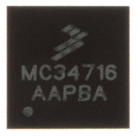
The 34716 is a highly integrated, space-efficient, low cost, dual synchronous
buck switching regulator with integrated N-channel power MOSFETs. It is a
high performance point-of-load (PoL) power supply with its second output
having the ability to track an external reference voltage. it provides a full power
supply solution for Double-Data-Rate (DDR) Memories.
Channel one provides a source only, 5.0 A drive capability, while channel two
can sink and source up to 3.0 A. With its high current drive capability, channel
one can be used to supply the VDDQ to the memory chipset. The second
channel’s ability to track a reference voltage provides an ideal means of
supporting the termination voltage (VTT) required by modern data buses such
as Double-Data-Rate (DDR) memory buses, including, but not limited to DDR,
DDR2, DDR3 and Low power DDR3/DDR4 memories. Both channels are
highly efficient with tight output regulation. The 34716 also provides a buffered
output reference voltage (VREFOUT) to the memory chipset.
The 34716 SMARTMOS device offers a variety of control, supervisory and
protection functions that simplify the implementation of complex designs. It is
housed in a Pb-free, thermally enhanced and space efficient 26-pin exposed
pad QFN.
Features
• 50 m integrated N-channel power MOSFETs
• Input voltage operating range from 3.0 to 6.0 V
• 1% accurate output voltages, ranging from 0.6 to 3.6 V
• The second output tracks 1/2 an external reference voltage
• 1% accurate buffered reference output voltage
• Programmable switching frequency range from 200 kHz to 1.0 MHz
• Programmable soft start timing for channel one
• Over-current limit and short-circuit protection on both channels
• Thermal shutdown
• Output over-voltage and under-voltage detection
• Active low power good output signal
• Active low standby and shutdown inputs
.
DUAL SWITCH-MODE DDR POWER
SUPPLY
EP SUFFIX
98ASA00702D
26-PIN QFN
34716
3.0 V to 6.0 V VIN
VDDQ
VIN
PVIN1
BOOT1
SW1
VOUT1
INV1
COMP1
PGND1
VDDI
FREQ
ILIM1
GND
PVIN2
VDDQ
VREFIN
BOOT2
SW2
VOUT2
VTT
INV2
DDR Memory
Chipset
COMP2
VREFOUT
PGND2
Termination
Resistors
VDDQ
VIN
Memory Bus
VREF
PG
STBY
SD
Figure 1. Simplified application diagram
© 2016 NXP B.V.
DDR Memory
Controller
MCU
�1
Orderable parts
Table 1. Orderable part variations
Part number
MC34716EP
Notes
Temperature (TA)
Package
(1)
-40 °C to 85 °C
26 pin QFN
Notes
1. To order parts in Tape & Reel, add the R2 suffix to the part number.
34716
2
NXP Semiconductors
�2
Internal block diagram
STBY
PG
System
Reset
M1
System
Control
Oscillator
FREQ
SD
Buck
Control
Logic
Thermal
Monitoring
Discharge
VBG
Bandgap
Regulator
ILIM2
ISENSE2
ISENSE1
Current
Monitoring
VDDI
Internal
Voltage
Regulator
ILIM1
ILIM1
VIN
BOOT1
M2
PVIN1
BOOT2
M3
PVIN2
VIN
VIN
M4
SW1
M6
Gate
Driver
ISENSE
FSW
FSW
Gate
I
Driver SENSE
M5
M7
–
–
+
+
–
+
PGND2
Error
Amplifier
–
VBG
INV1
COMP2
INV2
M8
M9
Discharge
Discharge
CHANNEL 1
CHANNEL 2
+
VOUT1
+
Error
Amplifier
PWM
Comparator
Ramp
Generator
PWM
Comparator
Ramp
Generator
PGND1
COMP1
SW2
M10
VREFIN
–
Discharge
VOUT2
GND
VREFOUT
Figure 2. Simplified internal block diagram
34716
NXP Semiconductors
3
�ILIM1
NC
FREQ
VIN
VIN
GND
VDDI
Pin connections
STBY
3
26 25 24 23 22 21 20 19
BOOT1 1
18 BOOT2
PVIN1
PVIN2
2
17
PVIN1
SW1
SW1
PGND1
Transparent
Top View
3
16
PIN 27
SW2
SW2
PGND2
4
15
PGND1
PGND2
14 VOUT2
8
9
10
11 12 13
VREFIN
VREFOUT
PG
SD
INV2
7
COMP2
6
COMP1
5
INV1
VOUT1
PVIN2
Figure 3. Pin connections
Section 5.2. "Functional pin description", page 14 provides a functional description of each pin.
Table 2. Pin definitions
Pin number
Pin name
Pin function
Formal name
Definition
1
BOOT1
Passive
Bootstrap
Channel 1 Bootstrap capacitor input pin
2
PVIN1
Supply
Power Input Voltage
Channel 1 Buck converter power input
3
SW1
Output
Switching Node
Channel 1 Buck converter switching node
4
PGND1
Ground
Power Ground
Channel 1 Buck converter and discharge MOSFETs power ground
Output Voltage
Discharge Path
Channel 1 Buck converter output voltage discharge pin
5
VOUT1
Output
6
INV1
Input
7
COMP1
Input
8
VREFIN
Input
9
VREFOUT
Output
Reference Voltage
Output
This is a buffered reference voltage output
10
PG
Output
Power Good Output
Signal
It is an active low open drain power good status reporting output
11
SD
Input
Shutdown Input
12
COMP2
Input
Buck Convertor
Compensation Input
13
INV2
Input
14
VOUT2
Output
Output Voltage
Discharge Path
Channel 2 Buck converter output voltage discharge pin
15
PGND2
Ground
Power Ground
Channel 2 Buck converter and discharge MOSFETs power ground
Error Amplifier Inverting
Channel 1 Buck converter error amplifier inverting input
Input
Buck Convertor
Compensation Input
Channel 1 Buck converter external compensation network input
Reference Voltage Input Voltage tracking reference voltage input
Shutdown mode input control pin
Channel 2 Buck converter external compensation network input
Error Amplifier Inverting
Channel 2 Buck converter error amplifier inverting input
Input
34716
4
NXP Semiconductors
�Table 2. Pin definitions (continued)
Pin number
Pin name
Pin function
Formal name
16
SW2
Output
Switching Node
17
PVIN2
Power
Power Input Voltage
Channel 2 Buck converter power input
18
BOOT2
Input
Bootstrap Input
Channel 2 Bootstrap capacitor input pin
19
ILIM1
Input
Soft Start Adjustment
Input
20
NC
None
No Connect
21
FREQ
Input
Frequency Adjustment
Input
22,23
VIN
Power
Input Supply Voltage
24
GND
Ground
25
VDDI
Output
26
STBY
Input
Standby Input
Standby mode input control pin
27
GND
Ground
Thermal Pad
Thermal pad for heat transfer. Connect the thermal pad to the analog ground and
the ground plane for heat sinking.
Signal Ground
Definition
Channel 2 Buck converter switching node
Channel 1 soft start adjustment
No internal connections to this pin
The buck converters switching frequency adjustment input
Power supply voltage of the IC
Analog ground of the IC
Internal Supply Voltage Internal supply voltage output
34716
NXP Semiconductors
5
�4
Electrical characteristics
4.1
Maximum ratings
Table 3. Maximum ratings
All voltages are with respect to ground unless otherwise noted. Exceeding these ratings may cause a malfunction or permanent damage
to the device.
Symbol
Ratings
Value
Unit
Notes
Electrical ratings
VIN
Input supply voltage (VIN) pin
0.3 to 7.0
V
PVIN
High-side MOSFET drain voltage (PVIN1, PVIN2) pins
0.3 to 7.0
V
VSW
Switching Node (SW1, SW2) Pins
0.3 to 7.0
V
BOOT1, BOOT2 pins (referenced to SW1, SW2 pins respectively)
0.3 to 7.0
V
-
PG, VOUT1, VOUT2, SD, and STBY pins
0.3 to 7.0
V
-
VDDI, FREQ, ILIM1, INV1, INV2, COMP1, COMP2, VREFIN, and VREFOUT pins
0.3 to 3.0
V
VBOOT - VSW
IOUT1
Channel 1 continuous output current
5.0
A
(2)
IOUT2
Channel 2 continuous output current
3.0
A
(2)
VESD1
VESD2
VESD3
ESD voltage
• Human body model
• Machine model (MM)
• Charge device model
V
(3)
40 to 85
°C
(4)
65 to 150
°C
2000
200
750
Thermal ratings
TA
Operating ambient temperature
TSTG
Storage temperature
TPPRT
Peak package reflow temperature during reflow
Note 6
°C
TJ(MAX)
Maximum junction temperature
150
°C
PD
Power dissipation (TA = 85 °C)
2.03
W
(5),(6)
(7)
Notes
2. Continuous output current capability so long as TJ is TJ(MAX).
3. ESD testing is performed in accordance with the Human Body Model (HBM) (CZAP = 100 pF, RZAP = 1500 ), the Machine Model (MM) (CZAP =
200 pF, RZAP = 0 ), and the Charge Device Model (CDM), Robotic (CZAP = 4.0 pF).
4. The limiting factor is junction temperature, taking into account power dissipation, thermal resistance, and heatsinking.
5. Pin soldering temperature limit is for 10 seconds maximum duration. Not designed for immersion soldering. Exceeding these limits may cause
malfunction or permanent damage to the device.
6. NXP’s Package Reflow capability meets Pb-free requirements for JEDEC standard J-STD-020C. For Peak Package Reflow Temperature and
Moisture Sensitivity Levels (MSL), Go to www.NXP.com, search by part number [e.g. remove prefixes/suffixes and enter the core ID to view all
orderable parts. (i.e. MC33xxxD enter 33xxx), and review parametrics.
7. Maximum power dissipation at indicated ambient temperature.
34716
6
NXP Semiconductors
�Table 3. Maximum ratings (continued)
All voltages are with respect to ground unless otherwise noted. Exceeding these ratings may cause a malfunction or permanent damage
to the device.
Symbol
Ratings
Value
Unit
Notes
Thermal resistance (8)
RJA
Thermal resistance, junction to ambient, single-layer board (1s)
93
°C/W
(9)
RJMA
Thermal resistance, junction to ambient, four-layer board (2s2p)
32
°C/W
(10)
RQJB
Thermal resistance, junction to board
13.6
°C/W
(11)
Notes
8. The PVIN, SW, and PGND pins comprise the main heat conduction paths.
9. Per SEMI G38-87 and JEDEC JESD51-2 with the single-layer board (JESD51-3) horizontal.
10. Per JEDEC JESD51-6 with the board (JESD51-7) horizontal. There are thermal vias connecting the package to the two planes in the board. (per
JESD51-5)
11. Thermal resistance between the device and the printed circuit board per JEDEC JESD51-8. Board temperature is measured on the top surface of
the board near the package.
4.2
Static electrical characteristics
Table 4. Static electrical characteristics
Characteristics noted under conditions 3.0 V VIN 6.0 V, 40 C TA 85 C, GND = 0 V, unless otherwise noted. Typical values
noted reflect the approximate parameter means at TA = 25 °C under nominal conditions, unless otherwise noted.
Symbol
Characteristic
Min.
Typ.
Max.
Unit
3.0
-
6.0
V
Notes
IC input supply voltage (VIN)
VIN
Input supply voltage operating range
IIN
Input DC supply current
(Normal mode: SD = 1 & STBY = 1, unloaded outputs)
-
-
35
mA
(12)
Input DC supply current
(Standby mode, SD = 1 & STBY = 0)
-
-
25
mA
(12)
Input DC supply current
(Shutdown mode, SD = 0 & STBY = X)
-
-
100
µA
(12)
2.35
2.5
2.65
V
CH 1 high-side MOSFET drain voltage range
2.5
-
6.0
V
Output voltage adjustment range
0.7
-
3.6
V
(13)
IINQ
IINOFF
Internal supply voltage output (VDDI)
VDDI
Internal supply voltage range
Channel 1 buck converter (PVIN1, SW1, PGND1, BOOT1, INV1, COMP1, ILIM1)
PVIN
VOUTHI1
Output voltage accuracy
1.0
-
1.0
%
(13), (14),
(15)
REGLN1
Line regulation
(Normal operation, VIN = 3.0 V to 6.0 V, IOUT1 = +5.0 A)
1.0
-
1.0
%
(13)
REGLD1
Load regulation
(Normal operation, IOUT1 = 0.0 A to 5.0 A)
1.0
-
1.0
%
(13)
-
0.7
-
V
(13)
-
VREF1
Error amplifier reference voltage
VUVR1
Output undervoltage threshold
8.0
-
1.5
%
VOVR1
Output overvoltage threshold
1.5
-
8.0
%
IOUT1
Continuous output current
-
-
5.0
A
ILIM1
Overcurrent limit
-
6.5
-
A
1.25
-
VDDI
V
-
8.5
-
A
VILIM1
ISHORT1
Soft start adjusting reference voltage range
Short-circuit current limit
34716
NXP Semiconductors
7
�Table 4. Static electrical characteristics (continued)
Characteristics noted under conditions 3.0 V VIN 6.0 V, 40 C TA 85 C, GND = 0 V, unless otherwise noted. Typical values
noted reflect the approximate parameter means at TA = 25 °C under nominal conditions, unless otherwise noted.
Symbol
Characteristic
Min.
Typ.
Max.
Unit
Notes
RDS(on)HS1
High-side N-CH power MOSFET (M4) RDS(on)
(IOUT1 = 1.0 A, VBOOT1 - VSW1= 3.3 V)
10
-
50
m
(13)
RDS(on)LS1
Low-side N-CH power MOSFET (M5) RDS(on)
(IOUT1 = 1.0 A, VIN = 3.3 V)
10
-
50
m
(13)
RDS(on)M2
M2 RDS(on)
(VIN = 3.3 V, M2 is on)
2.0
-
4.0
SW1 leakage current (standby and shutdown modes)
10
-
10
µA
PVIN1 pin leakage current
(Shutdown mode)
10
-
10
µA
Error amplifier DC gain
-
150
-
dB
(13)
Error amplifier unit gain bandwidth
-
3.0
-
MHz
(13)
ISW
IPVIN1
AEA
UGBWEA
Notes
12.
13.
14.
15.
Section “Modes of operation”, Page 18 has a detailed description of the different operating modes of the 34716
Design information only, this parameter is not production tested.
Overall output accuracy is directly affected by the accuracy of the external feedback network, 1% feedback resistors are recommended.
±1% is assured at room temperature.
Channel 1 buck converter (PVIN1, SW1, PGND1, BOOT1, INV1, COMP1, ILIM1) (continued)
SREA
Error amplifier slew rate
-
7.0
-
V/µs
(16)
(16)
OFFSETEA
Error amplifier input offset
3.0
0
3.0
mV
IINV1
INV1 pin leakage current
1.0
-
1.0
µA
TSDFET1
Thermal shutdown threshold
-
170
-
°C
(16)
TSDHYFET1
Thermal shutdown hysteresis
-
25
-
°C
(16)
CH 2 high-side MOSFET drain voltage range
2.5
-
6.0
V
Output voltage adjustment range
0.6
-
1.35
V
(16),(20)
Output voltage accuracy
1.0
-
1.0
%
(16), (17),
(18)
REGLN2
Line regulation (normal operation, VIN = 3.0 to 6.0 V, IOUT2 = ±3.0 A)
1.0
-
1.0
%
(16)
REGLD2
Load regulation (normal operation, IOUT2 = -3.0 to 3.0 A)
1.0
-
1.0
%
(16)
VREF2
Error amplifier common mode voltage range
0.0
-
1.35
V
(16), (19)
Channel 2 buck converter (PVIN2, SW2, PGND2, BOOT2, INV2, COMP2)
PVIN
VOUTHI2
-
VUVR2
Output undervoltage threshold
8.0
-
1.5
%
VOVR2
Output overvoltage threshold
1.5
-
8.0
%
IOUT2
Continuous output current
3.0
-
3.0
A
ILIM2
Overcurrent Limit (sinking and sourcing)
-
4.0
-
A
ISHORT2
Short-circuit current limit (sinking and sourcing)
-
6.5
-
A
RDS(on)HS2
High-side N-CH power MOSFET (M6) RDS(on)
• (IOUT2 = 1.0 A, VBOOT2 - VSW2= 3.3 V)
10
-
50
m
(16)
RDS(on)LS2
Low-side N-CH power MOSFET (M7) RDS(on)
• (IOUT2 = 1.0 A, VIN = 3.3 V)
10
-
50
m
(16)
RDS(on)M3
M3 RDS(on)
• (VIN = 3.3 V, M3 is on)
2.0
-
4.0
SW2 leakage current (standby and shutdown modes)
10
-
10
A
PVIN2 pin leakage current (standby and shutdown modes)
10
-
10
µA
ISW
IPVIN2
34716
8
NXP Semiconductors
�Table 4. Static electrical characteristics (continued)
Characteristics noted under conditions 3.0 V VIN 6.0 V, 40 C TA 85 C, GND = 0 V, unless otherwise noted. Typical values
noted reflect the approximate parameter means at TA = 25 °C under nominal conditions, unless otherwise noted.
Symbol
AEA
UGBWEA
SREA
Characteristic
Min.
Typ.
Max.
Unit
Notes
Error amplifier DC gain
-
150
-
dB
(16)
Error amplifier unit gain bandwidth
-
3.0
-
MHz
(16)
Error amplifier slew rate
-
7.0
-
V/µs
(16)
(16)
OFFSETEA
Error amplifier input offset
3.0
0
3.0
mV
IINV2
INV2 pin leakage current
1.0
-
1.0
µA
TSDFET2
Thermal shutdown threshold
-
170
-
°C
(16)
TSDHYFET2
Thermal shutdown hysteresis
-
25
-
°C
(16)
Notes
16.
17.
18.
19.
20.
Design information only, this parameter is not production tested.
Overall output accuracy is directly affected by the accuracy of the external feedback network. 1% feedback resistors are recommended
±1% is assured at room temperature
The 1% output voltage regulation is only guaranteed for a common mode voltage range greater than or equal to 0.6 V at room temperature
If a VOUT =0.6 V is desired, make sure VIN is kept below 3.6 V and the switching frequency FSW is lower than 500 kHz to allow enough room for
output regulation
34716
NXP Semiconductors
9
�Table 4. Static electrical characteristics (continued)
Characteristics noted under conditions 3.0 V VIN 6.0 V, 40 C TA 85 C, GND = 0 V, unless otherwise noted. Typical values
noted reflect the approximate parameter means at TA = 25 °C under nominal conditions, unless otherwise noted.
Symbol
Characteristic
Min.
Typ.
Max.
Unit
0.0
-
VDDI
V
VREFIN external reference voltage range
0.0
-
2.7
V
VREFOUT buffered reference voltage range
0.0
-
1.35
V
VREFOUT buffered reference voltage accuracy
1.0
-
1.0
%
Notes
Oscillator (FREQ)
VFREQ
Oscillator frequency adjusting reference voltage range
Tracking (VREFIN, VREFOUT, VOUT1, VOUT2)
VREFIN
VREFOUT
-
(21)
(22)
IREFOUT
VREFOUT buffered reference voltage current capability
0.0
-
8.0
mA
IREFOUTLIM
VREFOUT buffered reference voltage overcurrent limit
-
11
-
mA
RTDR(M10)
VREFOUT total discharge resistance
-
50
-
(21)
RTDR(M8)
VOUT1 total discharge resistance
-
50
-
(21)
RTDR(M9)
VOUT2 total discharge resistance
-
50
-
(21)
IVOUTLKG2
VOUT2 pin leakage current (standby mode, VOUT2 = 3.6 V)
1.0
-
1.0
µA
Control and supervisory (STBY, SD, PG)
VSTBYHI
STBY high level input voltage
2.0
-
-
V
VSTBYLO
STBY low level input voltage
-
-
0.4
V
RSTBYUP
STBY pin internal pull-up resistor
1.0
-
2.0
M
VSDHI
SD high level input voltage
2.0
-
-
V
VSDLO
SD low level input voltage
-
-
0.4
V
RSDUP
SD pin internal pull-up resistor
1.0
-
2.0
M
VPGLO
PG low level output voltage (IPG = 3.0 mA)
-
-
0.4
V
IPGLKG
PG pin leakage current (M1 is off, Pulled up to VIN)
-
-
1.0
µA
Notes
21. Design information only, this parameter is not production tested.
22. The 1% accuracy is only guaranteed for VREFOUT greater than or equal to 0.6 V at room temperature.
34716
10
NXP Semiconductors
�4.3
Dynamic electrical characteristics
Table 5. Dynamic electrical characteristics
Characteristics noted under conditions 3.0 V VIN 6.0 V, 40 C TA 85 C, GND = 0 V, unless otherwise noted. Typical values
noted reflect the approximate parameter means at TA = 25 °C under nominal conditions, unless otherwise noted.
Symbol
Characteristic
Min.
Typ.
Max.
Unit
Notes
Channel 1 buck converter (PVIN1, SW1, PGND1, BOOT1, INV1, COMP1, ILIM1)
tRISE1
Switching node (SW1) rise time
(PVIN = 3.3 V, IOUT1 = 5.0 A)
-
8.0
-
ns
(23)
tFALL1
Switching node (SW1) fall time (PVIN = 3.3 V, IOUT1 = 5.0 A)
-
5.0
-
ns
(23)
tOFFMIN
Minimum off time
-
150
-
ns
tONMIN
Minimum on time
-
0
-
ns
-
3.2
1.6
0.8
0.4
-
-
10
-
ms
Overcurrent limit retry timeout period
80
-
120
ms
Output undervoltage/overvoltage filter delay timer
5.0
-
25
µs
(24)
Soft start duration (normal mode)
ILIM1: 1.25 to 1.49 V
1.5 to 1.81 V
1.82 to 2.13 V
2.14 to 2.5 V
tSS1
tLIM1
tTIMEOUT1
tFILTER1
Overcurrent limit timer
ms
Channel 2 buck converter (PVIN2, SW2, PGND2, BOOT2, INV2, COMP2)
tRISE2
Switching node (SW2) rise time (PVIN = 3.3 V, IOUT2 = ±3.0 A)
-
28
-
ns
(23)
tFALL2
Switching node (SW2) fall time (PVIN = 3.3 V, IOUT2 = ±3.0 A)
-
12.0
-
ns
(23)
tOFFMIN
Minimum off time
-
150
-
ns
tONMIN
Minimum on time
-
180
-
ns
tSS2
Soft start duration (normal mode)
-
1.6
-
ms
tLIM2
Overcurrent limit timer
tTIMEOUT2
tFILTER2
Oscillator (FREQ)
-
10
-
ms
Overcurrent limit retry timeout period
80
-
120
ms
Output undervoltage/overvoltage filter delay timer
5.0
-
25
µs
-
1.0
-
MHz
200
-
1000
kHz
(25)
fSW
Oscillator default switching frequency (FREQ = GND)
fSW
Oscillator switching frequency range
Control and supervisory (STBY, SD, PG)
tPGRESET
PG reset delay
8.0
-
12
ms
tTIMEOUT
Thermal shutdown retry timeout period
80
-
120
ms
tOFFMIN
Minimum off time
-
150
-
ns
tONMIN
Minimum on time
-
100
-
ns
(23)
Notes
23. Design information only, this parameter is not production tested.
24. The regulator has the ability to enter into pulse skip mode when the inductor current ripple reaches the threshold for the LS zero detect, which has
a typical value of 500 mA.
25. Oscillator frequency tolerance is ±10%.
34716
NXP Semiconductors
11
�4.4
Electrical performance curves
VDDQ (VOUT1)
% Efficiency vs IOUT
100%
95%
VIN = 5V
Fs = 1MHz
TA=25°C
90%
Efficiency
85%
80%
75%
70%
65%
60%
55%
50%
0.0
0.5
1.0
1.5
2.0
2.5
3.0
3.5
4.0
4.5
5.0
IOUT, Amps
Figure 4. % Efficiency vs. IOUT
VTT (VOUT2)
% Efficien cy vs IOUT
100%
95%
90%
VIN = 5V
Fs = 1MHz
TA=25°C
Efficiency
85%
80%
75%
70%
65%
60%
55%
50%
0
0.5
1
1.5
2
2.5
3
IOUT, Amps
Figure 5. % Efficiency vs. IOUT
34716
12
NXP Semiconductors
�5
Functional description
5.1
Introduction
In modern microprocessor/memory applications, address command and control lines require system level termination to a voltage (VTT)
equal to 1/2 the memory supply voltage (VDDQ). Having the termination voltage at the midpoint ensures that the power supply maintains
symmetry when switching occurs. Also, the DDR SDRAM input receiver must have a reference voltage (VREF) that is free of any noise or
voltage variations. VREF is also equal to 1/2 VDDQ. Varying the VREF voltage effects the setup and hold time of the memory. To comply
with DDR requirements and to obtain the best performance, VTT and VREF must be tightly regulated to track 1/2 VDDQ across voltage,
temperature and noise margins. VTT must track any variations in the DC VREF value (VTT = VREF 40 mV), (See Figure 6) for a DDR system
level diagram.
The 34716 supplies the VDDQ, VTT and a buffered VREF output. To ensure compliance with DDR specifications, the VDDQ line is applied
to the VREFIN pin and divided by 2 internally through a precision resistor divider. This internal voltage is then used as the reference
voltage for the VTT output. The same internal voltage is also buffered so that the VREF voltage at the applications VREFOUT pin can be
used without an external resistor divider. The 34716 offers tight voltage regulation and power sequencing/tracking along with the ability
to handle DDR peak transient current requirements. It gives the user a complete DDR power supply solution with optimum performance.
Buffering the VREF output provides enhanced immunity to noise and load changes.
The 34716 uses a voltage mode synchronous buck switching converter topology with integrated low RDS(on) (50 m) N-channel power
MOSFETs to provide an output voltage accuracy of less than ±2.0%. It has a programmable switching frequency that operates at up to
1.0 MHz. The 34716 supplies 5.0 A maximum from one output and sinks and sources up to 3.0 A of continuous current from the other
output. It provides protection against output overcurrent, overvoltage, undervoltage and overtemperature conditions. It also protects the
system from short-circuit events. A power good output signal alerts the host when a fault occurs.
For boards that support the suspend-to-RAM (S3) and the suspend-to-disk (S5) states, the 34716 offers the STBY and the SD pins
respectively. Pulling any of these pins low, puts the IC in the corresponding state.
By integrating the control/supervisory circuitry along with the power MOSFET switches for the buck converter into a space-efficient
package, the 34716 offers a complete, small-size, cost-effective and simple solution to satisfy the needs of DDR memory applications.
Besides DDR memory termination, the 34716 also supports supply termination for other active buses and graphics card memory. It can
be used in Netcom/Telecom applications like servers and is suitable for desktop motherboards, game consoles, set top boxes, and high
end high definition TVs.
VDDQ
VTT
VDDQ
RT
RS
VREF
BUS
DDR Memory Controller
DDR Memory Input Receiver
Figure 6. DDR system level diagram
34716
NXP Semiconductors
13
�5.2
Functional pin description
5.2.1
Bootstrap input (BOOT1, BOOT2)
Bootstrap capacitor input pin. Connect a capacitor (as discussed in 7.7Bootstrap capacitor 27) between this pin and the SW pin of the
respective channel to enhance the gate of the high-side Power MOSFET during switching.
5.2.2
Power input voltage (PVIN1, PVIN2)
Buck converter power input voltage. This is the drain of the buck converter high-side power MOSFET.
5.2.3
Switching node (SW1, SW2)
Buck converter switching node. This pin is connected to the output inductor.
5.2.4
Power ground (PGND1, PGND2)
Buck converter and discharge MOSFETs power ground. It is the source of the buck converter low-side power MOSFET.
5.2.5
Compensation input (COMP1, COMP2)
Buck converter external compensation network connects to this pin. Use a type III compensation network.
5.2.6
Error amplifier inverting input (inv1, INV2)
Buck converter error amplifier inverting input. Connect the VDDQ voltage (channel 1) to INV1 pin through a resistor divider and connect
the VTT voltage (channel 2) directly to INV2 pin.
5.2.7
Output voltage discharge path (VOUT1, VOUT2)
Buck converters output voltage are connected to these pins. It only serves as the output discharge path once the SD signal is asserted.
5.2.8
Internal supply voltage output (VDDI)
This is the output of the internal bias voltage regulator. Connect a 1.0 µF, 6.0 V low ESR ceramic filter capacitor between this pin and the
GND pin. Filtering any spikes on this output is essential to the internal circuitry stable operation.
5.2.9
Signal ground (GND)
Analog ground of the IC. Internal analog signals are referenced to this pin voltage.
5.2.10 Input supply voltage (VIN)
IC power supply input voltage. Input filtering is required for the device to operate properly.
5.2.11 Power good output signal (PG)
This is an active low open drain output that is used to report the status of the device to a host. This output activates after a successful
power up sequence and stays active as long as the device is in normal operation and is not experiencing any faults. This output activates
after a 10 ms delay and must be pulled up by an external resistor to a supply voltage like VIN.
34716
14
NXP Semiconductors
�5.2.12 Standby input (STBY)
If this pin is tied to the GND pin, the device is set to standby mode. If left unconnected or tied to the VIN pin, the device is set to normal
mode. The pin has an internal pull-up of 1.5 M. This input accepts the S3 (suspend-to-RAM) control signal.
5.2.13 Shutdown input (SD)
If this pin is tied to the GND pin, the device is set to shutdown Mode. If left unconnected or tied to the vin pin, the device is set to normal
mode. the pin has an internal pull-up of 1.5 m. this input accepts the s5 (Suspend-To-Disk) control signal.
5.2.14 Reference voltage output (VREFOUT)
This is a buffered reference voltage output that is equal to 1/2 VREFIN. It has a 10 mA current drive capability. This output is used as the
VREF voltage rail and should be filtered against any noise. Connect a 0.1 µF, 6.0 V low ESR ceramic filter capacitor between this pin and
the GND pin and between this pin and VDDQ rail. VREFOUT is also used as the reference voltage for the buck converter error amplifier.
5.2.15 Reference voltage input (VREFIN)
The output of channel two tracks 1/2 the voltage applied at this pin.
5.2.16 Frequency adjustment input (FREQ)
The buck converters switching frequency can be adjusted by connecting this pin to an external resistor divider between VDDI and GND
pins. The default switching frequency (FREQ pin connected to ground, GND) is set at 1.0 MHz.
5.2.17 Channel 1 soft start adjustment input (ILIM1)
Channel one soft start can be adjusted by applying a voltage between 1.25 V and VDDI.
5.3
Functional internal block description
MC34716 - Functional Block Diagram
Internal Bias Circuits
System Control and Logic
Oscillator
Protection Functions
Control and
Supervisory Functions
Tracking and Sequencing
2 x Buck Converter
Figure 7. Block illustration
34716
NXP Semiconductors
15
�5.3.1
Internal bias circuits
This block contains all circuits that provide the necessary supply voltages and bias currents for the internal circuitry. It consists of:
• Internal voltage supply regulator: Supplies the VDDI voltage that is used to drive the digital/analog internal circuits. It is equipped with
a Power-On-Reset (POR) circuit that watches for the right regulation levels. External filtering is needed on the VDDI pin. This block
turns off during the shutdown mode.
• Internal bandgap reference voltage: Supplies the reference voltage to some of the internal circuitry.
• Bias circuit: Generates the bias currents necessary to run all of the blocks in the IC.
5.3.2
System control and logic
This block is the brains of the IC where the device processes data and reacts to it. Based on the status of the STBY and SD pins, the
system control reacts accordingly and orders the device into the right status. It also takes inputs from all of the monitoring/protection
circuits and initiates power-up or power-down commands. It communicates with the buck converter to manage the switching operation and
protects it against any faults.
5.3.3
Oscillator
This block generates the clock cycles necessary to run the IC digital blocks. It also generates the buck converters switching frequency.
The switching frequency can be programmed by connecting a resistor divider to the FREQ pin, between VDDI and GND pins (See
Figure 1).
5.3.4
Protection functions
This block contains the following circuits:
• Overcurrent limit and short-circuit detection: Monitors the output of the buck converters for overcurrent conditions and short-circuit
events and alerts the system control for further commands.
• Thermal limit detection: Monitors the temperature of the device for overheating events. If the temperature rises above the thermal
shutdown threshold, this block alerts the system control for further commands.
• Output overvoltage and undervoltage monitoring: This Monitors the buck converters output voltages to ensure they are within
regulation boundaries. If not, this block alerts the system control for further commands.
5.3.5
Control and supervisory functions
This block is used to interface with an outside host. It contains the following circuits:
• Standby control Input: An outside host can put the 34716 device into standby mode (S3 or suspend-to-RAM mode) by sending a
logic “0” to the STBY pin.
• Shutdown control Input: An outside host can put the 34716 device into shutdown mode (S5 or suspend-to-disk mode) by sending a
logic “0” to the SD pin.
• Power good output signal: The 34716 can communicate to an outside host that a fault has occurred by pulling the voltage on the PG
pin high through a pull-up resistor.
5.3.6
Tracking and sequencing
This block allows the output of channel 2 of the 34716 to track 1/2 the voltage applied at the VREFIN pin. This allows the VREF and VTT
voltages to track 1/2 VDDQ and assures that none of them are higher than VDDQ at any point during normal operating conditions. For powerdown during a shutdown (S5) mode, the 34716 uses internal discharge MOSFETs (M8, M9, and M10 on Figure 2) to discharge VDDQ, VTT,
and VREF respectively. These discharge MOSFETs are only active during shutdown mode. Using this block along with controlling the SD
and STBY pins makes the device suitable for power sequencing by controlling when to turn the 34716 outputs on or off.
34716
16
NXP Semiconductors
�5.3.7
Buck converter
This block provides the main function of the 34716: DC to DC conversion from an un-regulated input voltage to a regulated output voltage
used by the loads for reliable operation. The buck converter is a high performance, fixed frequency (externally adjustable), Synchronous
buck PWM voltage-mode control with a minimum on time of 100ns. It drives integrated 50 mN-channel power MOSFETs saving
board space and enhancing efficiency. The switching regulator output voltage is adjustable with an accuracy of less than ±2% to meet
DDR requirements. The regulator's voltage control loop is compensated using a type III compensation network, with external components
to allow for optimizing the loop compensation, for a wide range of operating conditions. A typical Bootstrap circuit with an internal PMOS
switch provides the voltage necessary to properly enhance the high-side MOSFET gate.
The 34716 is designed to address DDR memory power supplies. It provides a full power supply solution for DDR applications. The
integrated converter has the ability to supply up to 5.0 A out of channel 1 and sink and source up to 3.0 A of continuous current from
channel 2.
34716
NXP Semiconductors
17
�6
Functional device operation
6.1
Operational modes
SD = 0 &
STBY=x
VTT=VUVR2
VTT>=VOVR2
VTT
Over-voltage
VDDQ=ON
VTT=ON
VREF=ON
PG = 1
VIN < 3.0 V
Shutdown
VDDQ = Discharge
VTT = Discharge
VREF = Discharge
PG = 1
SD = 1 &
STBY=1
For>=10 ms
SD = 1 &
STBY=1
VDDQ=ILIM1
PG = 1
For>=10 ms
TIMEOUT=1
IOUT1>=ISHORT1
Figure 8. Operation modes diagram
6.1.1
Modes of operation
The 34716 has three primary modes of operation:
6.1.1.1
Normal mode
In normal mode, all functions and outputs are fully operational. To be in this mode, the VIN must be within its operating range. Both
shutdown and standby inputs must be pulled high, and there can be no faults present. This mode consumes the most amount of power.
6.1.1.2
Standby mode
This mode is predominantly used in desktop memory solutions where the DDR supply must be ACPI compliant (advanced configuration
and power interface). When this mode is activated by pulling the STBY pin low, VTT is put in high Z state, IOUT2 = 0 A while VDDQ and VREF
stay active. This is the S3 state suspend-to-RAM or self refresh mode and it is the lowest DRAM power state. In this mode, the DRAM
preserves the data. While in this mode, the 34716 consumes less power than in the normal mode, because the buck converter and most
of the internal blocks are disabled.
34716
18
NXP Semiconductors
�6.1.1.3
Shutdown mode
In this mode, activated by pulling the SD pin low, the chip is in a shutdown state and the outputs are all disabled and discharged. This is
the S4/S5 power state or suspend-to-disk state, where the DRAM loses all of its data content (no power supplied to the DRAM). The
reason for discharging the VTT and VREF lines is to ensure that, upon exiting, the shutdown mode, VTT and VREF are lower than VDDQ.
Otherwise VTT could remain floating high and be higher than VDDQ upon powering up. In this mode, the 34716 consumes the least amount
of power since almost all of the internal blocks are disabled.
6.1.2
Start-up sequence
When power is first applied, the 34716 checks the status of the SD and STBY pins. If the device is in a shutdown mode, no block powers
up and the output does not attempt to ramp. If the device is in a standby mode, only the VDDI internal supply voltage and the bias currents
are established and no further activities can occur. Once the SD and STBY pins are released to enable the device, the internal VDDI POR
signal is also released. The rest of the internal blocks are enabled, and the buck converters switching frequency and the VDDQ Soft start
values are determined by reading the FREQ and ILIM1 pins respectively. A soft start cycle is then initiated to ramp up the outputs. While
channel 1 buck converter uses an internal reference, channel 2 converter error amplifier uses the voltage on the VREFOUT pin (VREF) as
its reference voltage. VREF is equal to 1/2 VDDQ, where VDDQ is applied to the VREFIN pin. This way, the 34716 assures that VREF and
VTT voltages track 1/2 VDDQ to meet DDR requirements.
Soft start is used to prevent the output voltage from overshooting during startup. At initial startup, the output capacitor is at zero volts;
VOUT = 0 V. Therefore, the voltage across the inductor is PVIN during the capacitor charge phase which creates a very sharp di/dt ramp.
Allowing the inductor current to rise too high can result in a large difference between the charging current and the actual load current. This
could cause an undesired voltage spike once the capacitor is fully charged. The soft start is active each time the IC goes out of standby
or shutdown mode, power is recycled or after a fault retry.
To fully take advantage of soft starting, enable the VTT output before introducing VDDQ on the VREFIN pin. If this happens after a soft
start cycle expires and the VREFIN voltage has a high dv/dt, the output naturally tracks it immediately and ramp up with a fast dv/dt itself
(which defeats the purpose of soft starting). For reliable operation, it is best to have the VDDQ voltage available before enabling the VTT
output.
After a successful start-up cycle where the device is enabled, no faults have occurred and the output voltages have reached their
regulation point, the 34716 pulls the power good output signal low after a 10 ms reset delay. This indicates to the host that the device is
in normal operation.
6.1.3
Protection functions
The 34716 monitors the application for several fault conditions to protect the load from overstress. The reaction of the IC to these faults
ranges from turning off the outputs to just alerting the host that something is wrong. In the following paragraphs, each fault condition is
explained:
6.1.3.1
Output overvoltage
An overvoltage condition occurs once the output voltage goes higher than the rising overvoltage threshold (VOVR). In this case, the power
good output signal is pulled high, alerting the host that a fault is present, but the outputs stay active. To avoid erroneous overvoltage
conditions, a 20 µs filter is implemented. The buck converter uses its feedback loop to attempt to correct the fault. Once the output voltage
falls below the falling overvoltage threshold (VOVF), the fault is cleared and the power good output signal is pulled low. The device is then
back in normal operation. The condition is the same for both outputs.
6.1.3.2
Output undervoltage
An undervoltage condition occurs once the output voltage falls below the falling undervoltage threshold (VUVF). In this case, the power
good output signal is pulled high (alerting the host that a fault is present) ‘but the outputs stay active. To avoid erroneous undervoltage
conditions, a 20 µs filter is implemented. The buck converter uses its feedback loop to attempt to correct the fault. Once the output voltage
rises above the rising undervoltage threshold (VUVR), the fault is cleared and the power good output signal is pulled low. The device is
then back in normal operation. The condition is the same for both outputs.
34716
NXP Semiconductors
19
�6.1.3.3
Output overcurrent
This block detects overcurrent in the power MOSFETs of the buck converter. It is comprised of a sense MOSFET and a comparator for
each channel. The sense MOSFET acts as a current detecting device by sampling a ratio of the load current. That sample is compared
via the comparator with an internal reference to determine if the output is in overcurrent. If the peak current in the output inductor reaches
the overcurrent limit (ILIM), the converter starts a cycle-by-cycle operation to limit the current, and a 10 ms overcurrent limit timer (tLIM)
starts. The converter stays in this mode of operation until one of the following occurs:
• The current is reduced back to the normal level before tLIM expires. In this case normal operation is regained.
• tLIM expires without regaining normal operation, at which point the device turns off the output and the power good output signal is
pulled high. At the end of a timeout period of 100 ms (tTIMEOUT), the device attempts another soft start cycle.
• The device reaches the thermal shutdown limit (TSDFET) and turns off the output. The power good (PG) output signal is pulled high.
• The output current keeps increasing until it reaches the short-circuit current limit (ISHORT). See below for more details.
6.1.3.4
Short-circuit current limit
This block uses the same current detection mechanism as the overcurrent limit detection block. If the load current reaches the ISHORT
value, the device reacts by shutting down the output immediately. This is necessary to prevent damage in case of a permanent shortcircuit. Then, at the end of a timeout period of 100 ms (tTIMEOUT), the device attempts another soft start cycle.
6.1.3.5
Thermal shutdown
Each channel has its own thermal shutdown block. Thermal limit detection block monitors the temperature of the device and protects
against excessive heating. If the temperature reaches the thermal shutdown threshold (TSDFET), the converter output switches off and the
power good output signal indicates a fault by pulling high. The device stays in this state until the temperature has decreased by the
hysteresis value and then after a timeout period (tTIMEOUT) of 100 ms, the device automatically retries and the output goes through a soft
start cycle. If successful normal operation is regained, the power good output signal is asserted low.
34716
20
NXP Semiconductors
�Typical applications
7
8
9 10
SW2
ILIM1
16
15
GND
15
14
VOUT2
C11
0.1 F
VOUT2
11 12 13
INV1
COMP1
VREFIN
PVIN2
16
INV2
6
COMP2
PGND2
VOUT1
VOUT1
NC
FREQ
VIN
VIN
PGND1
VREFOUT
PGND2
VREFIN
5
17
SW2
PGND1
COMP1
4
SW2
0.1 F
17
SW2
MC34716
SW1
4
C27
0.1 F
PVIN2
SW1
3
GND
PVIN2
PVIN1
C15
18
BOOT2
PVIN1
SD
3
BOOT2
21 20 19
PG
2
SW1
24 23 22
BOOT1
2
PVIN1
x ILIM1
VDDI
1
VIN
FREQ
INV1
C28
SW1
0.1 F
STBY
C14
0.1 F
VDDI
STBY
26 25
BOOT1
GND
7
PG
INV2
SD
COMP2
C13
0.1 F
VREFOUT
C12
0.1 F
Compensation network SW1
Compensation network SW2
VO1
VO2
INV1
COMP1
C18
15 pF
R15
22 k
C19
0.75 nF
R14
560
INV2
C20
0.910 nF
R1
20 k
C21
20 pF
COMP2
R19
15 k
C22
1.8 nF
R2
12.7 k
Buck converter 1
SW1
D3
PMEG2010EA
_nopop
L1
1.0 H
C230
1.0 nF
R4
20 k
R2
17.4 k_nopop
Buck converter 2
Vo1_2
Vo1_1
R18
300
VO1
R20
4.7_nopop
C10 C24
C25
C26
100 F100 F
100 F
1 nF_nopop
SW2
D2
OMEG2010EA
_nopop
L1
1.5 H
Vo2_2
Vo2_1
VO2
R30
4.7_nopop
C7
C6
C8
C9
100 F 100 F
100 F
1 nF_nopop
Figure 9. Typical application
34716
NXP Semiconductors
21
�I/O signals
GND
GND
PVIN1
VO1
3
2
1
PVIN2
VO2
3
2
1
VM
VIN
3
2
1
GND
VIN capacitors
VIN
J2
PGOOD LED
VM
VIN
C17
10 F
C16
0.1 F
R7
1k
J3
R8
10 k
D1
LED
VMASTER
R9
10 k
LED
J4
ILIM1, FREQ
Jumpers
VO1
VMASTER
STBY_nopop
LED
1
2
2
1
VMASTER
1
3
5
7
9
J1
2
4
6
8
10
VREFIN
VDDI
R16
10 k
PG
STBY
ILIM1
R22
10 k_nopop
SD
CON10A
SD
VDDI
R12
10 k_nopop
FREQ
R11
10 k
PVIN2 capacitors
PVIN1 capacitors
PVIN1
PVIN2
C1
0.1 F
C2
1 F
C30
0.1 F
C3
C4
C5
100 F 100 F 100 F
C31
1 F
C32
C33
C29
1002 F 100 F 100 F
Trimpots nopop
VDDI
ILIM1
R21
POT_50 k_nopop
FREQ
R6
POT_50 k_nopop
Figure 10. Typical application
34716
22
NXP Semiconductors
�7.1
Configuring the output voltage:
Channel 1 of the 34716 is a general purpose DC-DC converter. The resistor divider to the -INV1 node is responsible for setting the output
voltage, according to the following equation:
R1
VOUT VREF
1
R2
Where VREF is the internal VBG=0.7 V.
Channel 2 is a DDR specific voltage power supply, and the output voltage is given by the equation:
VTT
V REFIN
2
Where VREFIN is equal to VDDQ.
7.2
Switching frequency configuration
The switching frequency has a value of 1.0 MHz when the FREQ pin is connected to the GND. If the smallest frequency value of 200 kHz
is desired, then connect the FREQ pin to VDDI. To program the switching frequency to another value, an external resistor divider must
be connected to the FREQ pin to achieve the voltages given by Table 7.3.
34716
NXP Semiconductors
23
�7.3
Frequency selection
Frequency
7.4
Voltage applied to pin FREQ
200
2.341 – 2.500
253
2.185 – 2.340
307
2.029 – 2.184
360
1.873 – 2.028
413
1.717 – 1.872
466
1.561 – 1.716
520
1.405 – 1.560
573
1.249 – 1.404
627
1.093 – 1.248
680
0.936 – 1.092
733
0.781 – 0.936
787
0.625 – 0.780
840
0.469 – 0.624
893
0.313 – 0.468
947
0.157 – 0.312
1000
0.000 – 0.156
Soft start adjustment
Table 6 shows the voltage that should be applied to the ILIM1 pin to get the desired sort start timing on channel 1 only.
Table 6. Soft start configurations
Soft start [ms]
Voltage applied to ILIM
3.2
1.19 – 1.49 V
1.6
1.50 – 1.81 V
0.8
1.82 – 2.13 V
0.4
2.14 – 2.50 V
RFQH
CVDDI
RIH
RIL
RFQL
VDDI
FREQ
ILIM1
GND
Figure 11. Resistor divider for frequency and soft ftart adjustment
34716
24
NXP Semiconductors
�7.5
Selecting inductor
Inductor calculation process is the same for both channels. The equation is the following:
(Vout I out * ( Rds (on) _ ls r _ w))
I out
Vout
Maximum Off Time Percentage
1
Vin _ max
L D'MAX T
D'MAX
T
Switching Period
Rds (on) _ ls
Drain – to – Source
Resistance of FET
r_w
I OUT 0.4 * I OUT
Winding Resistance of Inductor
Output Current Ripple
If channel 1 is serving as the power supply for channel 2, locate the LC poles at different frequencies in order to ensure that the input
impedance of the second converter is always higher than the output impedance of the first converter (thus ensuring system stability). This
is achieved by selecting different values for L1 and L2 slightly higher than the calculated value.
34716
NXP Semiconductors
25
�7.6
Selecting the output filter capacitor
For the output capacitor, the following considerations are most important and not the actual Farad value: the physical size, the ESR of the
capacitor and the voltage rating.
Calculate the minimum output capacitor using the following formula:
Co
I OUT * dt _ I _ rise
TR _ V _ dip
Transient response percentage:
TR_%
(Use a recommended value of 2 to 4% to assure a good transient response.)
Maximum transient voltage:
TR_V_dip = VOUT*TR_%
Maximum current step:
Iout _ step
(Vin _ min Vout ) * D _ max
Fsw * L
Inductor current rise time:
dt _ I _ rise
T * I OUT
I OUT _ step
The following formula are helpful for finding the maximum allowed ESR.
ESRmax
VOUT * Fsw * L
VOUT (1 D min)
The effects of the ESR is often neglected by the designers and may present a hidden danger to the ultimate supply stability. Poor
quality capacitors have widely disparate ESR values, which can make the closed loop response inconsistent.
34716
26
NXP Semiconductors
�7.7
Bootstrap capacitor
The bootstrap capacitor is needed to supply the gate voltage for the high-side MOSFET. This N-channel MOSFET needs a voltage
difference between its gate and source to be able to turn on. The high-side MOSFET source is the SW node, so it is not at ground and it
is floating and shifting in voltage. Applying a voltage directly to the gate of the high-side that is referenced to ground is not sufficient.
Instead, the voltage must be referenced to the SW node. This is why the bootstrap capacitor is needed. This capacitor charges during the
high- side off time. Since the low-side is on during that time, the SW node and the bottom of the bootstrap capacitor are connected to
ground, and the top of the capacitor is connected to a voltage source. The capacitor charges up to that voltage source (for example 5.0 V).
Now when the low- side MOSFET switches off and the high-side MOSFET switches on, the SW nodes rise to VIN, and the voltage on the
boot pin becomes VCAP + VIN. The gate of the high-side has VCAP across it and can stay enhanced. A 0.1 f capacitor is a good value for
this bootstrap element.
7.8
Type III compensation network
To meet contemporary demands, power supplies must often offer accurate and tight output voltage regulation. A high DC gain is required
to accomplish this. However, high gain increases the possibility of instability in the power supply. To minimize the threat of power supply
instability, compensation is added to the internal error amplifier to counteract some of the gains and phases contained in the control-tooutput transfer function. The Type III compensation network used for 34716 is comprised of two poles: One integrator and one high
frequency to cancel the zero generated from the ESR of the output capacitor and two zeros to cancel the two poles generated from the
LC filter as shown in Figure 12.
SWx
Lx
VOUTx
RSx
COx
R1x
CSx
INVx
CXx
RFx
R2x
CFx
COMPx
Figure 12. Type III compensation network
1. Choose a value for R1 (R2 only applies to channel 1).
2. Consider a crossover frequency of one tenth the switching frequency. Set the zero pole frequency to Fcross/10.
FP 0
1
1
FCROSS
10
2 * R1C F
1
CF
2 * R1 FPO
34716
NXP Semiconductors
27
�3. Knowing the LC frequency, the frequency of zero 1 and zero 2 in the compensation network is equal to FLC.
FLC
1
FZ 1 FZ 2
2 LX COX
1
2 * RF C F
FZ 1
FZ 2
1
2 * R1C S
This gives the following result:
RF
1
2 * C F FZ 1
CS
1
2 * R1 FZ 2
4. Calculate RS by placing the first pole at the ESR zero frequency.
1
FP1
2 * Co X * ESR
1
1
RS
FP1
2 * FP1C S
2 * RS C S
FESR
5. Equating pole 2 to 5 times the crossover frequency to achieve a faster response and a proper phase margin:
5 F CROSS = F
1
--------------------------------------P2 =
CF CX
2 R F -------------------CF + Cx
CX
CF
2 * R F C F FP 2 1
34716
28
NXP Semiconductors
�7.9
Tracking configurations
The 34716 allows default Ratiometric tracking on channel 2 by connecting VDDQ to the VREFIN pin. It has an internal resistor divider that
allows an output of VDDQ/2.
7.10
Layout guidelines
The layout of any switching regulator requires careful consideration. First, there are high di/dt signals present, and the traces carrying
these signals need to be kept as short and as wide as possible to minimize the trace inductance and therefore reduce the voltage spikes
they can create. To do this, requires an understanding of the major current carrying loops. See Figure 13. Place these loops and their
associated components in a way that minimizes the loop size and prevents coupling to other parts of the circuit. Also, to minimize noise
coupling, route the current-carrying power traces and their associated return traces so that they run adjacent to one another. If sensitive
traces must cross the current carrying traces, place them perpendicular to one another to reduce field interaction.
Second, carefully consider the placement of small signal components that connect to sensitive nodes. The critical small signal
components are the ones associated with the feedback circuit. The high-impedance input of the error amp is especially sensitive to noise,
and the feedback. So place compensation components as far from the switch node and as close to the input of the error amplifier as
possible. Other critical small signal components include the bypass capacitors for VIN, VREFIN, and VDDI. Locate the bypass capacitors
as close to the pin as possible.
The use of a multi-layer printed circuit board is recommended. Dedicate one layer, usually the layer under the top layer, as a ground plane.
Make all critical component ground connections with vias to this layer. Make sure that the power grounds (PGND1 and PGND2) are
connected directly to the ground plane and not routed through the thermal pad or analog ground. Dedicate another layer as a power plane
and split this plane into local areas for common voltage nets.
Use a dedicated trace to connect the IC input supply (VIN) to the input supply. This prevents noise on the buck regulator's power inputs
(PVIN1 and PVIN2) from injecting switching noise into the IC’s analog circuitry.
In order to effectively transfer heat from the top layer to the ground plane and other layers of the printed circuit board, thermal vias must
be used in the thermal pad design. Five to nine vias should be spaced evenly and have a finished diameter of 0.3 mm.
VIN1
PVIN1
VIN2and
and 23
Loop Curr ent
HS ON
HS
SW1
SW2and
and 2
3
SW1
SD
Loop Curr ent
HS ON
HS
Loop
Current
SD ON
Loop
Current
LS ON
LS
GND2and
and23
PGND1
BUCK
CONVERTER 1
Buck
converter
1 and 2
BUCK
CONVERTER
2 and 3
Figure 13. Current loop
34716
NXP Semiconductors
29
�8
Packaging
8.1
Packaging dimensions
34716
30
NXP Semiconductors
�34716
NXP Semiconductors
31
�34716
32
NXP Semiconductors
�9
Revision history
Revision
Date
Description of Changes
1.0
2/2006
•
•
Pre-release version
Implemented Revision History page
2.0
2/2007
•
•
•
Initial release
Converted format from Market Assessment to Product Preview
Major updates to the data, form, and style
•
•
•
•
•
•
•
•
Changed Feature from 2% to 1%, relabeled to include soft start
Change references for 45 m Integrated N-Channel Power MOSFETs to 50 m
Removed Machine Model in Maximum ratings
Changed Input DC supply current, Input DC supply current, and Input DC supply current
Added CH 1 high-side MOSFET drain voltage range
Changed Output voltage accuracy
Changed Soft start adjusting reference voltage range and Short-circuit current limit
Changed High-side N-CH power MOSFET (M4) RDS(on) and Low-side N-CH power MOSFET
(M5) RDS(on)
Changed M2 RDS(on) and PVIN1 pin leakage current
Added CH 2 high-side MOSFET drain voltage range
Changed Output voltage accuracy
Changed Short-circuit current limit (sinking and sourcing)
Changed High-side N-CH power MOSFET (M6) RDS(on) and Low-side N-CH power MOSFET
(M7) RDS(on)
Changed M3 RDS(on) and PVIN2 pin leakage current (standby and shutdown modes)
Changed VREFOUT buffered reference voltage accuracy, VREFOUT buffered reference voltage
current capability, and VREFOUT buffered reference voltage overcurrent limit
Changed STBY pin internal pull-up resistor and SD pin internal pull-up resistor
Changed Soft start duration (normal mode)
Changed Overcurrent limit retry timeout period and Output undervoltage/overvoltage filter delay
timer
Changed Oscillator default switching frequency (FREQ = GND), PG reset delay, and Thermal
shutdown retry timeout period
Changed definition for Channel 1 soft start adjustment input (ILIM1)
Changed drawings in Typical application
Changed table for Soft start adjustment
Removed PC34716EP/R2 from the ordering information and added MC34716EP/R2
Changed data sheet status to Advance Information
•
•
•
•
•
3.0
5/2007
•
•
•
•
•
•
•
•
•
•
•
•
4.0
12/2008
•
•
•
Made changes to Switching Node (SW1, SW2) Pins, BOOT1, BOOT2 pins (referenced to SW1,
SW2 pins respectively), Output undervoltage threshold, Output overvoltage threshold, Both
channels of High-side N-CH power MOSFET (M4) RDS(on), Both channels of Low-side N-CH
power MOSFET (M5) RDS(on), Charge device model
Added Machine model (MM), Both channels of SW2 leakage current (standby and shutdown
modes), Both channels of (Error amplifier DC gain, Error amplifier unit gain bandwidth, Error
amplifier slew rate, Error amplifier input offset)
Fixed drawing for Type III compensation network
Added pin 27 to Figure 3 and the Pin definitions
Added the section Layout guidelines
•
5.0
4/2012
•
Changed typical for Minimum on time 11
6.0
12/2014
•
Updated case outline (changed 98ASA10728D to 98ASA00702D) as per PCN 16331
7.0
3/2015
•
Added note (19) to Static electrical characteristics
8.0
4/2016
•
•
Minimum output voltage for Channel 2 extended to 0.6 V
Updated document style and format
34716
NXP Semiconductors
33
�How to Reach Us:
Information in this document is provided solely to enable system and software implementers to use NXP products.
Home Page:
NXP.com
There are no expressed or implied copyright licenses granted hereunder to design or fabricate any integrated circuits
Web Support:
http://www.nxp.com/support
anyproducts herein. NXP makes no warranty, representation, or guarantee regarding the suitability of its products for
based on the information in this document. NXP reserves the right to make changes without further notice to
any particular purpose, nor does NXP assume any liability arising out of the application or use of any product or circuit,
and specifically disclaims any and all liability, including without limitation, consequential or incidental damages.
"Typical" parameters that may be provided in NXP data sheets and/or specifications can and do vary in different
applications, and actual performance may vary over time. All operating parameters, including "typicals," must be
validated for each customer application by the customer's technical experts. NXP does not convey any license under
its patent rights nor the rights of others. NXP sells products pursuant to standard terms and conditions of sale, which
can be found at the following address:
http://www.nxp.com/terms-of-use.html.
NXP, the NXP logo, Freescale, the Freescale logo and SMARTMOS are trademarks of NXP B.V. All other product or
service names are the property of their respective owners. All rights reserved.
© 2016 NXP B.V.
Document Number: MC34716
Rev. 8.0
4/2016
�