Freescale Semiconductor
Technical Data
Document Number: MC34933
Rev. 3.0, 9/2014
1.4 A Dual H-Bridge Driver
Compatible with 3.0 V Logic
34933
The 34933 is a two channel H-Bridge driver aimed at the digital
camera market. There are a variety of applications containing bipolar
step motors and/or brush DC motors, such as Auto Focus control for
the digital camera lens. The 34933 uses Freescale's proprietary
SMARTMOS process to deliver a low-power device, with a maximum
quiescent current of 100 A for the motor drive supply and 400A for
the control logic supply.
The 34933 VM supply operates from 2.0 V to 7.0 V using an internal
charge pump, with independent control of each H-Bridge driver via the
MCU (IN1A, IN1B, IN2A, IN2B). The 34933 has a low total RDS(on) of
1.0 (max. at 25 °C). Shoot-through current protection is a built-in
feature for the 34933 device.
The 34933 has four operation modes: forward, reverse, brake, and
tri-state (high-impedance). The 34933 employs a VCC detection circuit
to sense when the logic supply switches to an off-state with a maximum
current of 1.0 A to extend battery life. The H-Bridge drivers can be
independently pulse width modulated up to 200 kHz for speed/ torque
and/or current control. Note that tri-state mode of H-Bridge drivers can
occur when either VCC detect is low or the thermal detect is active.
Features
•
•
•
•
•
•
•
•
•
•
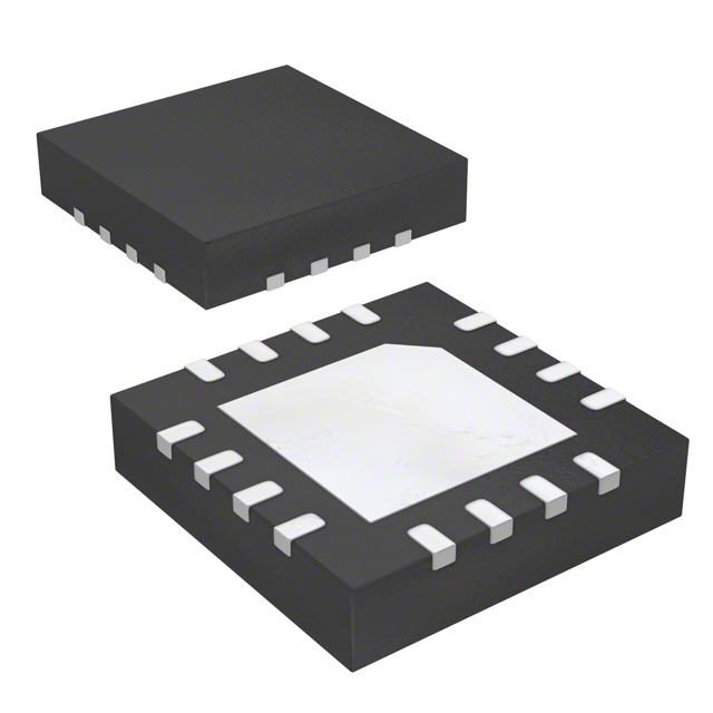
H-BRIDGE DRIVER
EP SUFFIX (Pb-FREE)
98ASA00717D
16-PIN UQFN
ORDERING INFORMATION
Device
(For Tape and Reel, add an R2
Suffix)
Temperature
Range (TA)
Package
MC34933EP
-20 °C to 85 °C
16-UQFN
Built-in 2-channel H-Bridge driver
H-Bridge operation voltage 2.0 V to 7.0 V
Max. load output current 1.0 A at TA = 25 °C
Low total RDS(ON) 0.8 (typ), 1.0 (max.) @ TA = 25 °C peak
Dual channel parallel driver, RDS(ON) 0.4 (typ.). max. DC current 1.4 A
PWM control input frequency up to 200 kHz
Built-in shoot-through current prevention circuit
Built-in charge pump circuit (external cap type)
VCC low voltage detection for logic power supply voltage
Thermal detection for H-Bridge driver
3.0 V
5.0 V
34933
VCC
VG
MCU
VM1
VM2
CH
OUT1A
CL
OUT1B
IN1A
IN1B
IN2A
IN2B
OUT2A
OUT2B
PGND1
PGND2
Figure 1. 34933 Simplified Application Diagram
© Freescale Semiconductor, Inc., 2012-2014. All rights reserved.
M
Stepper
Motor
�INTERNAL BLOCK DIAGRAM
INTERNAL BLOCK DIAGRAM
VG = VM+VCC
VM
VCC
VCC
VG
VCC DETECTION
CH
CHARGE PUMP
THERMAL DETECTION
VCCdet
tdet
CL
VM1
VCC
VCCdet
VG
VCC
VCC
High-side Driver
tdet
VCC
OUT1A
IN1A
OUT1B
IN1B
CONTROL
LOGIC
IN2A
LEVEL SHIFTER
PRE-DRIVER
Low-side Driver
PGND1
VM2
High-side Driver
IN2B
OUT2A
OUT2B
Low-side Driver
PGND2
* VM1 and VM2 are connected internally. Both VM1 and VM2 must be tied together on the PCB.
PGND1 and PGND2 are connected internally. Both PGND1 and PGND2 must be tied together on the PCB.
Figure 2. 34933 Simplified Internal Block Diagram
34933
2
Analog Integrated Circuit Device Data
Freescale Semiconductor
�PIN CONNECTIONS
OUT1B
VM1
CH
CL
PIN CONNECTIONS
16
15
14
13
OUT1A 1
12 VG
17
Exposed
Pad
PGND1 2
PGND2 3
11 VCC
10 IN1A
OUT2A 4
5
6
7
8
OUT2B
VM2
IN2A
IN2B
9 IN1B
Figure 3. 34933 Pin Connections
Table 1. 34933 Pin Definitions
Pin
Number
Pin Name
Pin Function
Formal Name
1
OUT1A
Output
H-Bridge Output 1A
2
PGND1
Power supply
Power Ground 1
Power supply grounds for the 34933 device. Refer to the application
diagram for recommended layout.
3
PGND2
Power supply
Power Ground 2
Power supply grounds for the 34933 device. Refer to the application
diagram for recommended layout.
4
OUT2A
Output
H-Bridge Output 2A
Output A of H-Bridge channel 2
5
OUT2B
Output
H-Bridge Output 2B
Output B of H-Bridge channel 2
6
VM2
7
IN2A
Input
Logic Input Control 2A
Logic input control of OUT2A
8
IN2B
Input
Logic Input Control 2B
Logic input control of OUT2B
9
IN1B
Input
Logic Input Control 1B
Logic input control of OUT1B
10
IN1A
Input
Logic Input Control 1A
Logic input control of OUT1A
11
VCC
12
VG
Output
Charge Pump Output
Capacitor
13
CL
Input/Output
Charge Pump Capacitor 1
Low-side charge pump capacitor connection
14
CH
Input/Output
Charge Pump Capacitor 2
High-side charge pump capacitor connection
15
VM1
16
OUT1B
17
(1)
Power supply Motor Drive Power Supply 2
Power supply Control Logic Power Supply
Power supply Motor Drive Power Supply 1
Output
Exposed Pad Power supply
H-Bridge Output 1B
EP
Definition
Output A of H-Bridge channel 1.
Power supply pins for the 34933 motor drive circuitry. Refer to the
application diagram for recommended layout.
Power supply for the control logic circuitry.
Charge pump output pin connected to an external capacitor. The VG
voltage is the sum of the VCC and VM power supplies.
Power Supply pins for the 34933 motor drive circuitry. Refer to the
application diagram for recommended layout.
Output B of H-Bridge channel 1
The exposed pad is connected to ground plane via the exposed pad
solder pad. Note the primary purpose of the exposed pad for 34933
is thermal heat dissipation. Therefore, adequate thermal vias should
be included in the PCB design.
Notes
1. Exposed pad is used as a heat sink. Connect it to the power ground through four thermal vias where the area is wide.
34933
Analog Integrated Circuit Device Data
Freescale Semiconductor
3
�ELECTRICAL CHARACTERISTICS
MAXIMUM RATINGS
ELECTRICAL CHARACTERISTICS
MAXIMUM RATINGS
Table 2. Maximum Ratings
All voltages are with respect to ground unless otherwise noted. Exceeding these ratings may cause a malfunction or
permanent damage to the device.
Ratings
Symbol
Value
Unit
VCC
-0.5 to +6.0
V
VM
-0.5 to +7.5
V
VCC Level Pin Voltage - IN1A, IN1B, IN2A, IN2B
Vpin1
-0.5 to +5.5
V
VM Level Pin Voltage - OUT1A, OUT1B, OUT2A, OUT2B, CL
Vpin2
-0.5 to +7.5
V
VM+VCC Level Pin Voltage - CH, VG
Vpin3
-0.5 to +13.5
V
Motor Drive Maximum Load Current, TA = 85 °C
ILOAD_DC_MD
0.7
A
Motor Drive Maximum Load Current, TA = 25 °C
ILOAD_DC_MD
1.0
A
ILOAD_PEAK_MD
1.4
A
PD
1.0
W
ELECTRICAL RATINGS
Control Logic Power Supply Voltage
Motor Drive Power Supply
Motor Drive Maximum Peak Load
Power
ESD
Current(3)
Dissipation(4)
Voltage(2)
VESD
V
4000
Human Body Model (HBM)
Machine Model (MM)
350
Charge Device Model (CDM)
1000
THERMAL RATINGS
Operating Temperature Range
TA
-20 to +85
°C
Operating Junction Temperature
TJ
150
°C
TSTG
-65 to +150
°C
RJC
23
C/W
TPPRT
Note 7
°C
Storage Temperature Range
THERMAL RESISTANCE
Thermal Resistance, Junction to Case(5)
Peak Package Reflow Temperature During
Reflow(6), (7)
Notes
2.
ESD testing is performed in accordance with the Human Body Model (HBM) (CZAP = 100 pF, RZAP = 1500 ), the Machine Model (MM)
(CZAP = 200 pF, RZAP = 0 ), and the Charge Device Model (CDM), Robotic (CZAP = 4.0 pF).
3.
Peak time is for 10 ms pulse width at 200 ms intervals. TA = 25°C.
4.
RJA = 50 °C/W, in case of 2s2p printed circuit board that defined on SEMI JEDEC JESD51- 3 and JESD51-6.
5.
6.
Thermal resistance between the die and the case top surface as measured by the cold plate method (MIL SPEC-883 Method 1012.1).
Pin soldering temperature limit is for 10 seconds maximum duration. Not designed for immersion soldering. Exceeding these limits may
cause malfunction or permanent damage to the device.
Freescale’s Package Reflow capability meets Pb-free requirements for JEDEC standard J-STD-020C. For Peak Package Reflow
Temperature and Moisture Sensitivity Levels (MSL), go to www.freescale.com, search by part number [e.g. remove prefixes/suffixes and
enter the core ID to view all orderable parts. (i.e. MC33xxxD enter 33xxx), and review parametrics.
7.
34933
4
Analog Integrated Circuit Device Data
Freescale Semiconductor
�ELECTRICAL CHARACTERISTICS
STATIC AND DYNAMIC ELECTRICAL CHARACTERISTICS
STATIC AND DYNAMIC ELECTRICAL CHARACTERISTICS
Table 3. Static and Dynamic Electrical Characteristics
Characteristics noted under conditions, VM = 5.0 V, VCC = 3.0 V, unless otherwise noted. Typical values noted reflect the
approximate parameter means at TA = 25 °C under nominal conditions, unless otherwise noted.
Characteristic
Symbol
Min
Typ
Max
Unit
Motor Drive Power Supply Voltage
VM
2.0
5.0
7.0
V
Control Logic Power Supply Voltage
VCC
2.7
3.0
5.5
V
Driver Quiescent Supply Current (IN1A, IN1B,IN2A, IN2B = L)
IQM
-
72
100
-
114
400
-
350
800
POWER SUPPLY
No Signal Input
Logic Quiescent Supply Current (IN1A, IN1B, IN2A, IN2B = L)
IQVCC
No Signal Input
Control Logic Power Supply Operating Current (IN1A, IN2A = L, IN1B, IN2B = 200kHz)
Charge Pump Target Voltage
IVCC
Charge Pump Switching Frequency
4.2
7.6
12.0
4.45
7.8
12.3
4.7
8.0
12.5
-
130
400
-
-
1.0
-
150
-
-
0.4
0.45
-
0.43
0.51
us
IQM_VCD = L
VM = 5.0 V, VCC = 0 V
FQP
uA
V
TVGON
Charge pump is enabled in VCC > VCCDET
Driver Quiescent Supply Current at VCCDET = L
uA
VG
VM = 2.0 V, VCC = 2.7 V, ILOAD = 0A
VM = 5.0 V, VCC = 3.0 V, ILOAD = 0A
VM = 7.0 V, VCC = 5.5 V, ILOAD = 0A
Charge Pump Wake-up Time
uA
uA
kHz
H-BRIDGE DRIVER
H-Bridge Driver High/Low-side Driver On-Resistance 1
H-Bridge Driver High/Low-side Driver On-Resistance 2 (8)
Duty of input signal = 50 %
-
0.39
0.43
-
0.41
0.48
-
0.49
0.58
VF
If = 100 mA
Input Pulse Frequency (INA/B)
0.62
RON6
VCC = 3.0 V, ISINK = 700 mA, TA = 85 °C
H-Bridge Driver Output Body Diode Forward Voltage
0.51
RON5
VCC = 3.0 V, ISINK = 700 mA, TA = 25 °C
H-Bridge Driver High/Low-side Driver On-Resistance 6 (8)
RON4
VCC = 3.0 V, ISINK = 100 mA, TA = 25 °C
H-Bridge Driver High/Low-side Driver On-Resistance 5 (8)
RON3
VCC = 2.7 V, ISINK = 700 mA, TA = 85 °C
H-Bridge Driver High/Low-side Driver On-Resistance 4
RON2
VCC = 2.7 V, ISINK = 700 mA, TA = 25 °C
H-Bridge Driver High/Low-side Driver On-Resistance 3 (8)
RON1
VCC = 2.7 V, ISINK = 100 mA, TA = 25 °C
V
-
0.8
1.2
-
-
200
FIN
kHz
Notes
8. Guaranteed by design
34933
Analog Integrated Circuit Device Data
Freescale Semiconductor
5
�ELECTRICAL CHARACTERISTICS
STATIC AND DYNAMIC ELECTRICAL CHARACTERISTICS
Table 3. Static and Dynamic Electrical Characteristics
Characteristics noted under conditions, VM = 5.0 V, VCC = 3.0 V, unless otherwise noted. Typical values noted reflect the
approximate parameter means at TA = 25 °C under nominal conditions, unless otherwise noted.
Characteristic
Symbol
Min
Typ
Max
-
0.1
0.5
-
0.1
0.5
0.7
-
-
-
-
0.5
Unit
H-BRIDGE DRIVER (CONTINUED)
H-Bridge Output Propagation Delay Time for OUTA/B (H to L)
tPDHL
us
RLOAD = (1.0 k) between OUTA and OUTB (refer to Figure 4) (IN1A, IN2A = L, IN1B,
IN2B = 200 kHz)
H-Bridge Output Propagation Delay Time for OUTA/B (L to H)
tPDLH
us
Rload = (1.0 k ) between OUTA and OUTB (refer to Figure 4) (IN1A, IN2A = L, IN1B,
IN2B = 200 kHz)
H-Bridge Output Pulse Width
tPW
us
RLOAD = 20 between OUTA and OUTB, Input Pulse Width = 1.0 s, 50% to 50%,
tPW: 50% to 50% (refer to Figure 5)
H-Bridge Output Propagation Delay Time (Hi-Z to H) (8)
tPDZH
us
RLOAD = 100 k to 1/2*VM, CLOAD = 0 pF, tPDZH 50% to 75%
H-Bridge Output Propagation Delay- Time (H to Hi-Z) (8)
tPDHZ
us
RLOAD = 100 k to 1/2*VM, CLOAD = 0 pF, tPDHZ 75% to 50%
-
-
2.0
CONTROL LOGIC
High Level Input Voltage (IN1A, IN1B, IN2A, IN2B)
VIH
V
VCC = 2.7 V ~ 5.5 V
Low Level Input Voltage (IN1A, IN1B, IN2A, IN2B)
-
VCCx0.3
uA
9
-
20
-1.0
-
-
-
-
1.0
-
-
1.0
VCCDET
2.0
2.2
2.4
V
VCCDETHYS
0.05
0.1
0.3
V
TDET
150
170
190
°C
TDETHYS
10
20
30
°C
IIL
uA
tR
us
VCC = 2.7 V to 5.5 V
Input Pulse Fall Time (IN1A, IN1B, IN2A, IN2B)
IIH
VCC = 2.7 V to 5.5 V
Input Pulse Rise Time (IN1A, IN1B, IN2A, IN2B)
V
VTERMAINAL1 = 3.0 V
Low Level Input Current (IN1A, IN1B, IN2A, IN2B)
-
VIL
VCC = 2.7 V ~ 5.5 V
High Level Input Current (IN1A, IN1B, IN2A, IN2B)
VCCx0.7
tF
us
VCC = 2.7 V to 5.5 V
DETECTOR
VCC Detection Voltage (refer to Figure 6)
VCC Detection hysteresis Voltage (refer to Figure 6)
Thermal Detection Temperature
(9)
Thermal Detection Hysteresis Temperature
(9)
Notes
9. Guaranteed by design
34933
6
Analog Integrated Circuit Device Data
Freescale Semiconductor
�ELECTRICAL CHARACTERISTICS
TIMING DIAGRAMS
TIMING DIAGRAMS
VCC
IN1AIN1/2A
/ IN2A
IN1/2B
IN1B / IN2B
50%
tPDLH
tPDHL
VM
OUT1A
/ OUT2A
OUT1/2A
OUT1B
/ OUT2B
OUT1/2B
90%
10%
Figure 4. tPDLH and tPDHL Timing
VCC
IN1A / IN2A
IN1B / IN2B
50%
tPW
VM
OUT1A / OUT2A
OUT1B / OUT2B
50%
Figure 5. tPW Timing
Table 4. Truth Table
INPUT
Vccdet
Tdet
OUTPUT
IN1A
IN1B
OUT1A
OUT1B
IN2A
IN2B
OUT2A
OUT2B
L
X
X
X
Z
Z
H
L
L
L
L
L
H
L
H
L
H
L
H
L
L
H
L
H
H
L
H
H
Z
Z
H
H
X
X
Z
Z
H - High
L - Low
Z - High-impedance
X - Don’t Care
Figure 6 and Figure 7 show the timing charts of input and output signals
34933
Analog Integrated Circuit Device Data
Freescale Semiconductor
7
�ELECTRICAL CHARACTERISTICS
TIMING DIAGRAMS
VM
Vc cdet
Vcc det
VC C
Vccdet-Vc cdet hys
Vc cdet-Vcdethys
vcc det
(internal signal)
VG
TVGON
T VGON
IN1A/IN2A
IN1/2A
IN1B/IN2B
IN1/2B
OUT1A/OUT2A
OUT1/2A
Hi-Z
OUT2A/OUT2B
OUT1/ 2B
Hi-Z
Brake
Brake
H i-Z
Hi-Z
Hi-Z
H i-Z
Brake
Hi-Z
Brake
Hi-Z
Hi-Z
Figure 6. Timing Chart of Input and Output Signal (VCCDET case)
VM
Vc cdet
Vcc det-Vccdethys
VCC
vc cdet
(internal signal)
Tet
Temperat ure
T et-T dethys
t det
(internal signal)
VG
TVGON
IN1A/IN2A
IN1/2A
IN1B/IN2B
I N1/2B
O UT1/2A
OUT1A/OUT2A
Hi-Z
OUT2A/OUT2B
O UT1/2B
H i-Z
Brake
Brake
Hi-Z
Hi-Z
Hi-Z
Hi-Z
Brake
Hi-Z
Brake
Hi-Z
Figure 7. Timing Chart of Input and Output Signal (tDET case)
34933
8
Analog Integrated Circuit Device Data
Freescale Semiconductor
�FUNCTIONAL DESCRIPTION
FUNCTIONAL PIN DESCRIPTION
FUNCTIONAL DESCRIPTION
FUNCTIONAL PIN DESCRIPTION
LOGIC SUPPLY (VCC)
MOTOR DRIVE POWER SUPPLY (VM1 AND VM2)
The VCC pin carries the logic supply voltage and current
into the logic sections of the IC. VCC has an under-voltage
threshold. If the supply voltage drops below the undervoltage threshold, the output power stage switches to a tristate condition. When the supply voltage returns to a level
that is above the threshold, the power stage automatically
resumes normal operation according to the established
condition of the input pins.
The VM pins carry the main supply voltage and current into
the power sections of the IC. This supply then becomes
controlled and/or modulated by the IC as it delivers the power
to the loads attached between the output pins. All VM pins
must be connected together on the Printed Circuit Board
(PCB).
LOGIC INPUT CONTROL (IN1A, IN1B, IN2A, AND
IN2B)
These logic input pins control each H-Bridge output. IN1A
logic HIGH = OUT1A HIGH. However, if all inputs are HIGH,
the output bridges are both tri-stated (refer to Table 4, Truth
Table).
H-BRIDGE OUTPUT (OUT1A, OUT1B, OUT2A, AND
OUT2B)
These pins provide connection to the outputs of each of
the internal H-Bridges (See Figure 2, 34933 Simplified
Internal Block Diagram).
CHARGE PUMP (CL AND CH)
These two pins, the CL and CH, connect to the external
bucket capacitors required by the internal charge pump. The
typical value for the bucket capacitors is 0.1 F.
POWER GROUND (PGND)
Power ground pins must be tied together on the PCB and
connected to the common ground plane.
LOGIC GROUND (EXPOSED PAD)
The Exposed Pad is connected to the PCB Ground plane
through vias by soldering. Note the primary purpose of the
Exposed pad for 34933 is thermal heat dissipation.
Therefore, adequate thermal vias should be included in the
PCB design. The exposed pad should be connected to the
common ground plane.
VOLTAGE DETECTION AND THERMAL LIMIT DETECTION
The 34933 has the VCC Low Voltage Detection (Vccdet)
and the Thermal Detection (TDET). VCC Low Voltage Detection is designed to shutdown of IC functions when VCC
becomes lower than specified voltage. Thermal Detection
operates when the IC temperature exceeds specified value
and stop H-Bridge operation. Table 5 shows block status of
34933 by each condition. VCC is the control logic power
supply for 34933. The system begins to operate when VCC >
VCCDET (Typ. 2.2 V).
Table 5. Block Status
Operation mode
Vccdet
Tdet
Charge Pump
H-Bridge Driver
1
L
X
Disable
Disable
2
H
L
Enable
Enable
3
H
H
Enable
Disable
H - High
L - Low
X - Don’t Care
34933
Analog Integrated Circuit Device Data
Freescale Semiconductor
9
�TYPICAL APPLICATION
TYPICAL APPLICATION
Figure 8 shows a typical application using the 34933. The internal charge pump of this device is powered from the VCC supply.
Therefore, care must be taken to ensure VCC is a high enough value to provide sufficient gate-source voltage for the high-side
MOSFETs when VM > VCC (e.g., VM = 5.0 V, VCC = 3.0 V), in order to ensure full enhancement of the high-side MOSFET
channels.
The 34933 can be configured in several applications. The figure below shows the 34933 in a typical Slave Node Application.
VM
CL
C
VG
0.1F
13
CH
14
16
*1
15
Motor
VM1
OUT1B
C
0.1F
HL
CVM
22F
*1
*1
Exposed pad
11
3
10
4
9
5
OUT2A
17
VG
VCC
VCC
IN 1A
1F
CVC
IN 1B
*1
8
PGND2
2
12
7
PGND1
1
6
OUT1A
IN2B
IN2A
VM2
OUT2B
Motor
MCU
interface:
VCC level
*1
*1 - It is recommend to use low resistance copper PCB traces between
VM & VCC ground and the PGND1/PGND2 pins.
Figure 8. Typical Application
34933
10
Analog Integrated Circuit Device Data
Freescale Semiconductor
�PCB LAYOUT
PCB LAYOUT
When designing a printed circuit board (PCB), connect
sufficient capacitance between power supplies (VM & VCC)
and ground pins to ensure proper filtering from transients. For
all high-current paths, use wide copper traces and the
shortest possible distances. Note that capacitors should be
placed as close to the 34933 as possible to maximize the
filtering capability of each capacitor.
Additionally, care must be taken to avoid CEMF spikes
induced when inductive currents accumulate at the VM
supply. The typical method of snubbing inductive spikes
includes connecting a Zener diode or capacitor at the supply
pin (VM).
34933
Analog Integrated Circuit Device Data
Freescale Semiconductor
11
�PACKAGING
PACKAGE DIMENSIONS
PACKAGING
PACKAGE DIMENSIONS
Package dimensions are provided in package drawings. To find the most current package outline drawing, go to
www.freescale.com and perform a keyword search for the drawing’s document number.
Table 6.
Package
16-PIN UQFN
Suffix
EP
Package Outline Drawing Number
98ASA00717D
34933
12
Analog Integrated Circuit Device Data
Freescale Semiconductor
�PACKAGING
PACKAGE DIMENSIONS
.
34933
Analog Integrated Circuit Device Data
Freescale Semiconductor
13
�PACKAGING
PACKAGE DIMENSIONS
34933
14
Analog Integrated Circuit Device Data
Freescale Semiconductor
�PACKAGING
PACKAGE DIMENSIONS
34933
Analog Integrated Circuit Device Data
Freescale Semiconductor
15
�REVISION HISTORY
REVISION HISTORY
REVISION
2.0
3.0
DATE
DESCRIPTION OF CHANGES
7/2010
•
Initial Release.
12/2013
•
•
•
No technical changes
Revised back page
Updated document properties
9/2014
•
•
Changed 98A to 98ASA00717D
Update format
34933
16
Analog Integrated Circuit Device Data
Freescale Semiconductor
�How to Reach Us:
Information in this document is provided solely to enable system and software implementers to use Freescale products.
Home Page:
freescale.com
There are no express or implied copyright licenses granted hereunder to design or fabricate any integrated circuits based
Web Support:
freescale.com/support
Freescale reserves the right to make changes without further notice to any products herein. Freescale makes no
on the information in this document.
warranty, representation, or guarantee regarding the suitability of its products for any particular purpose, nor does
Freescale assume any liability arising out of the application or use of any product or circuit, and specifically disclaims any
and all liability, including without limitation consequential or incidental damages. “Typical” parameters that may be
provided in Freescale data sheets and/or specifications can and do vary in different applications, and actual performance
may vary over time. All operating parameters, including “typicals,” must be validated for each customer application by
customer’s technical experts. Freescale does not convey any license under its patent rights nor the rights of others.
Freescale sells products pursuant to standard terms and conditions of sale, which can be found at the following address:
freescale.com/SalesTermsandConditions.
Freescale and the Freescale logo are trademarks of Freescale Semiconductor, Inc., Reg. U.S. Pat. & Tm. Off.
SMARTMOS is a trademark of Freescale Semiconductor, Inc. All other product or service names are the property of their
respective owners.
© 2014 Freescale Semiconductor, Inc.
Document Number: MC34933
Rev. 3.0
9/2014
�