Freescale Semiconductor
Advance Information
Document Number: MC34982
Rev. 1.0, 9/2014
Single Intelligent High-current
Self-protected High-side Switch
(2.0 mOhm)
34982
The 34982 is a self-protected 2.0 mOhm high-side switch replacing
electromechanical relays, fuses, and discrete devices in power management
applications. The 34982 is designed for harsh environments and includes selfrecovery features. The device is suitable for loads with high inrush current, as
well as motors and all types of resistive and inductive loads.
Programming, control, and diagnostics are implemented via the serial peripheral
interface (SPI). A dedicated parallel input is available for alternate and pulsewidth modulation (PWM) control of the output. SPI-programmable fault trip
thresholds allow the device to be adjusted for optimal performance in the
application.
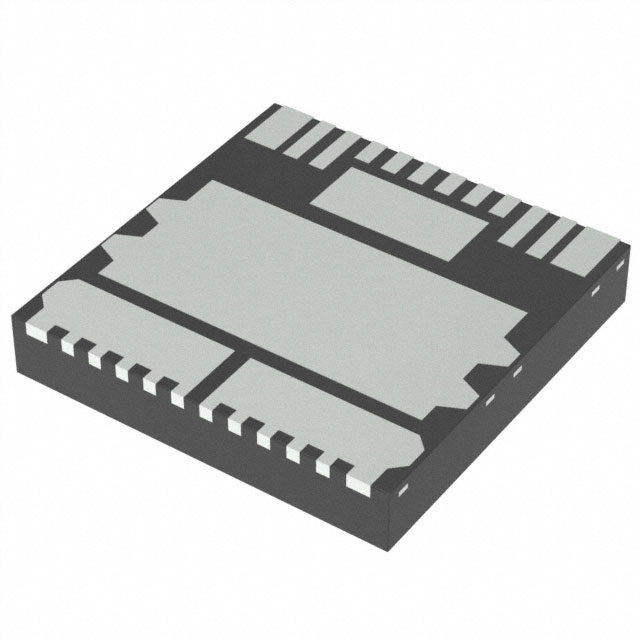
The 34982 is packaged in a power-enhanced 12 x 12 mm nonleaded PQFN
package with exposed tabs and powered by SMARTMOS technology.
HIGH-SIDE SWITCH
BOTTOM VIEW
Features
•
•
•
•
Single 2.0 m max. high-side switch with parallel input or SPI control
6.0 V to 27 V operating voltage with standby currents < 5.0 A
Output current monitoring with two SPI-selectable current ratios
SPI control of overcurrent limit, overcurrent fault blanking time, output OFF
open load detection, output ON/OFF control, watchdog timeout, slewrates, and fault status reporting
• SPI status reporting of overcurrent, open and shorted loads,
overtemperature shutdown, undervoltage and overvoltage shutdown, Failsafe pin status, and program status
• Enhanced -16 V reverse polarity VPWR protection
VDD
VDD
VDD
FK SUFFIX
SCALE
1:1
98ARL10521D
16-PIN PQFN
Applications
•
•
•
•
Low-voltage factory automation
DC motor or solenoid
Resistive and inductive loads
Low-voltage industrial lighting
VPWR
34982
VDD
I/O
FS
I/O
WAKE
SO
SI
SCLK
MCU
VPWR
GND
SCLK
CS
CS
SI
SO
I/O
RST
I/O
IN
HS
LOAD
A/D
CSNS
FSI
GND
GND
PWR GND
Figure 1. 34982 Simplified Application Diagram
* This document contains certain information on a new product.
Specifications and information herein are subject to change without notice.
© Freescale Semiconductor, Inc., 2014. All rights reserved.
�ORDERABLE PARTS
ORDERABLE PARTS
Table 1. Orderable Part Variations
Part Number
MC34982CHFK
(1)
Temperature (TA)
Package
-40 °C to 125 °C
16 PQFN
Notes
1. To order parts in Tape & Reel, add the R2 suffix to the part number.
34982
2
Analog Integrated Circuit Device Data
Freescale Semiconductor
�INTERNAL BLOCK DIAGRAM
INTERNAL BLOCK DIAGRAM
VDD
VPWR
Internal
Regulator
IUP
CS
Overvoltage
Protection
Programmable
Switch Delay
0–525 ms
SO
SPI
3.0 MHz
SI
SCLK
FS
IN
RST
WAKE
VIC
Selectable Slew
Rate Gate Drive
HS
Selectable Overcurrent
High Detection
150 A or 100 A
Logic
Selectable Overcurrent
Low Detection
Blanking Time
0.15–155 ms
IDWN
Selectable
Overcurrent
Low Detection
15–50 A
Open Load
Detection
RDWN
Overtemperature
Detection
Programmable
Watchdog
310–2500 ms
Selectable
Output Current
Recopy
1/5400 or 1/40000
VIC
IUP
FSI
GND
CSNS
Figure 2. 34982 Simplified Internal Block Diagram
34982
Analog Integrated Circuit Device Data
Freescale Semiconductor
3
�PIN CONNECTIONS
PIN CONNECTIONS
4
3 2
CSNS
RST
WAKE
6 5
IN
FS
CS
8 7
FSI
SI
SCLK
SO
VDD
NC
12 11 10 9
1
13
GND
TRANSPARENT
TOP VIEW
14
VPWR
15
HS
16
HS
Figure 3. 34982 Pin Connections
Functional descriptions of many of these pins can be found in the Functional Pin Description section beginning on page 16.
Table 2. Pin Definitions
Pin
Number
Pin Name
Pin Function
Formal Name
Definition
1
CSNS
Output
Output Current
Monitoring
This pin is used to output a current proportional to the high-side output current and
used externally to generate a ground-referenced voltage for the microcontroller to
monitor output current.
2
WAKE
Input
Wake
3
RST
Input
Reset (Active Low)
4
IN
Input
Direct Input
The input pin is used to directly control the output.
5
FS
Output
Fault Status
(Active Low)
This is an open drain configured output requiring an external pull-up resistor to VDD
for fault reporting.
6
FSI
Input
Fail-safe Input
The value of the resistance connected between this pin and ground determines the
state of the output after a watchdog timeout occurs.
7
CS
Input
Chip Select
(Active Low)
This input pin is connected to a chip select output of a master microcontroller (MCU).
8
SCLK
Input
Serial Clock
This input pin is connected to the MCU providing the required bit shift clock for SPI
communication.
9
SI
Input
Serial Input
This is a command data input pin connected to the SPI Serial Data Output of the
MCU or to the SO pin of the previous device in a daisy chain of devices.
10
VDD
Input
Digital Drain Voltage
(Power)
11
SO
Output
Serial Output
This output pin is connected to the SPI Serial Data Input pin of the MCU or to the SI
pin of the next device in a daisy chain of devices.
12
NC
NC
No Connect
This pin may not be connected.
13
GND
Ground
Ground
This pin is used to input a Logic [1] signal in order to enable the watchdog timer
function.
This input pin is used to initialize the device configuration and fault registers, as well
as place the device in a low current sleep mode.
This is an external voltage input pin used to supply power to the SPI circuit.
This pin is the ground for the logic and analog circuitry of the device.
34982
4
Analog Integrated Circuit Device Data
Freescale Semiconductor
�PIN CONNECTIONS
Table 2. Pin Definitions (continued)
Pin
Number
Pin Name
Pin Function
Formal Name
Definition
14
VPWR
Input
Positive Power Supply
This pin connects to the positive power supply and is the source input of operational
power for the device.
15, 16
HS
Output
High-side Output
Protected high-side power output to the load. Output pins must be connected in
parallel for operation.
34982
Analog Integrated Circuit Device Data
Freescale Semiconductor
5
�ELECTRICAL CHARACTERISTICS
MAXIMUM RATINGS
ELECTRICAL CHARACTERISTICS
MAXIMUM RATINGS
Table 3. Maximum Ratings
All voltages are with respect to ground, unless otherwise noted.
Symbol
Rating
Value
Unit
Notes
Operating Voltage Range
Steady-state
-16 to 41
V
VDD Supply Voltage
-0.3 to 5.5
V
VIN, RST, FSI,
CSNS, SI, SCLK, Input/Output Voltage
CS, FS
- 0.3 to 7.0
V
(1)
- 0.3 to VDD + 0.3
V
(1)
ELECTRICAL RATINGS
VPWR
VDD
VSO
SO Output Voltage
ICL(WAKE)
WAKE Input Clamp Current
2.5
mA
ICL(CSNS)
CSNS Input Clamp Current
10
mA
IHS
Output Current
60
A
VHS
Output Voltage
Positive
Negative
41
-15
V
ECL
Output Clamp Energy
34982C
1.0
VESD1
VESD3
ESD Voltage
Human Body Model (HBM)
Charge Device Model (CDM)
Corner Pins (1, 12, 15, 16)
All Other Pins (2, 11, 13, 14)
(2)
J
(3)
V
(4)
± 2000
±750
±500
Notes
1. Exceeding this voltage limit may cause permanent damage to the device.
2. Continuous high-side output current rating so long as maximum junction temperature is not exceeded. Calculation of maximum output current
using package thermal resistance is required.
3. Active clamp energy using single-pulse method (L = 16 mH, RL = 0, VPWR = 12 V, TJ = 150 °C).
4.
ESD1 testing is performed in accordance with the Human Body Model (HBM) (CZAP = 100 pF, RZAP = 1500 ESD3 testing is performed in
accordance with the Charge Device Model (CDM), Robotic (CZAP = 4.0 pF).
34982
6
Analog Integrated Circuit Device Data
Freescale Semiconductor
�ELECTRICAL CHARACTERISTICS
MAXIMUM RATINGS
Table 3. Maximum Ratings (continued)
All voltages are with respect to ground, unless otherwise noted.
Symbol
Rating
Value
Unit
Notes
Operating Temperature
Ambient
Junction
- 40 to 125
- 40 to 150
C
(5)
TSTG
Storage Temperature
- 55 to 150
C
RJC
RJA
Thermal Resistance
Junction-to-Case
Junction-to-Ambient
VPWRUV
FS State
VPWRUV > VPWR >
UVPOR
SPI Fault
Register UVF
Bit
Output State
UVPOR > VPWR >
2.5 V
FS State
FS State
2.5 V > VPWR > 0 V
SPI Fault
Register UVF
Bit
Comments
UV fault
is latched
Typical value; not guaranteed
While VDD remains within specified range.
= IN is equivalent to IN direct input or IN_spi SPI input.
REVERSE VOLTAGE
The output survives the application of reverse voltage as low as -16 V. Under these conditions, the output’s gate is enhanced to keep the
junction temperature less than 150 °C. The ON resistance of the output is fairly similar to that in the Normal mode. No additional passive
components are required. If more than one output is driving a DC motor with an external freewheeling diode in parallel to the load, a direct
current passes through this diode and the internal high-side switch in case of reverse voltage.
34982
Analog Integrated Circuit Device Data
Freescale Semiconductor
21
�FUNCTIONAL DEVICE OPERATION
PROTECTION AND DIAGNOSIS FEATURES
34982
4
Figure 10. Reverse Voltage Protection
As shown in Figure 10, it is essential to protect this power line. The proposed solution is an external N-channel low-side with the gate tied
to supply voltage through a resistor.
GROUND DISCONNECT PROTECTION
In the event the 34982 ground is disconnected from load ground, the device protects itself and safely turns OFF the output regardless the
state of the output at the time of disconnection. A 10 k resistor needs to be added between the WAKE pin and the rest of the circuitry in
order to ensure that the device turns off in case of ground disconnect and to prevent this pin to exceed its maximum ratings.
34982
22
Analog Integrated Circuit Device Data
Freescale Semiconductor
�FUNCTIONAL DEVICE OPERATION
LOGIC COMMANDS AND REGISTERS
FUNCTIONAL DEVICE OPERATION
LOGIC COMMANDS AND REGISTERS
SPI PROTOCOL DESCRIPTION
The SPI interface has a full duplex, three-wire synchronous data transfer with four I /O lines associated with it: Serial Clock (SCLK), Serial
Input (SI), Serial Output (SO), and Chip Select (CS).
The SI / SO pins of the 34982 follow a first-in first-out (D7 / D0) protocol with both input and output words transferring the most significant
bit (MSB) first. All inputs are compatible with 5.0 V CMOS logic levels.
The SPI lines perform the following functions:
SERIAL CLOCK (SCLK)
The SCLK pin clocks the internal shift registers of the 34982 device. The serial input pin (SI) accepts data into the input shift register on
the falling edge of the SCLK signal while the serial output pin (SO) shifts data information out of the SO line driver on the rising edge of
the SCLK signal. It is important that the SCLK pin be in a logic LOW state whenever CS makes any transition. For this reason, it is
recommended that the SCLK pin be in a Logic [0] state whenever the device is not accessed (CS Logic [1] state). SCLK has an active
internal pull-down, IDWN. When CS is Logic [1], signals at the SCLK and SI pins are ignored and SO is tri-stated (high-impedance). (See
Figure 11 and Figure 12.)
SERIAL INTERFACE (SI)
This is a serial interface (SI) command data input pin. SI instruction is read on the falling edge of SCLK. An 8-bit stream of serial data is
required on the SI pin, starting with D7 to D0. The internal registers of the 34982 are configured and controlled using a 4-bit addressing
scheme, as shown in Table 9. Register addressing and configuration are described in Table 10. The SI input has an active internal pulldown, IDWN.
SERIAL OUTPUT (SO)
The SO pin is a tri-stateable output from the shift register. The SO pin remains in a high-impedance state until the CS pin is put into a
Logic [0] state. The SO data is capable of reporting the status of the output, the device configuration, and the state of the key inputs. The
SO pin changes states on the rising edge of SCLK and reads out on the falling edge of SCLK. Fault and input status descriptions are
provided in Table 16.
CHIP SELECT (CS)
The CS pin enables communication with the master microcontroller (MCU). When this pin is in a Logic [0] state, the device is capable of
transferring information to and receiving information from the MCU. The 34982 latches in data from the input shift registers to the
addressed registers on the rising edge of CS. The device transfers status information from the power output to the shift register on the
falling edge of CS. The SO output driver is enabled when CS is Logic [0]. CS should transition from a Logic [1] to a Logic [0] state only
when SCLK is a Logic [0]. CS has an active internal pull-up, IUP.
CSB
CS
SCLK
SI
SO
SO
D7
OD7
D6
OD6
D5
OD5
D4
OD4
D3
OD3
D2
OD2
D1
OD1
D0
OD0
1. RST
a in
Logic
[1]1 state
duringthethe
above
operation.
Notes 1.
RSTis is
RSTB
a logic
state during
above
operation.
NOTES:
2.
D0, D1,relate
D2, ...,toand
relaterecent
to the most
recent
ordered
entryinto
of data
the SPSS
2. D7:D0
theD7most
ordered
entry
of data
theinto
device.
3.
OD0, OD1,relate
OD2, ...,
first 8 bits
of ordered
fault and
data
outdevice.
3. OD7:OD0
to and
the OD7
first relate
8 bitstoofthe
ordered
fault
and status
datastatus
out of
the
of the device.
Figure 11. Single 8-Bit Word SPI Communication
34982
Analog Integrated Circuit Device Data
Freescale Semiconductor
23
�FUNCTIONAL DEVICE OPERATION
LOGIC COMMANDS AND REGISTERS
C
S B
CS
SCLK
S
C L K
SIS
I
D 7
S O
SO
N O T E S :
D 6
O D 7
1 .
D 5
O D 6
R
R SST T B
D 2
O D 5
D 1
O D 2
D 0
O D 1
D 7 *
O D 0
D 6 *
D 7
D 6
D 5 *
D 2 *
D 5
D 1 *
D 2
D 1
D 0 *
D 0
is in a lo g ic 1 s t a t e d u r in g t h e a b o v e o p e r a t io n .
2 .
0 , Logic
D 1 , D 2[1]
, . .state
. , a n d during
D 7 r e l a the
t e t oabove
t h e m ooperation.
s t r e c e n t o r d e r e d e n tr y o f d a ta in to th e S P S S
Notes 1. RST
isD a
3 .
O D 0 , O D 1 , O D 2 , . . . , a n d O D 7 r e la t e t o t h e f ir s t 8 b it s o f o r d e r e d f a u lt a n d s t a t u s d a t a o u t o f t h e d e v ic e .
2. D7:D0
4 .
O relate
D 0 , O Dto
1 , the
O D most
2 , . . . , arecent
n d O D ordered
7 r e p r e s eentry
n t t h e of
f i r sdata
t 8 b into
i t s o f the
o r d device.
e r e d fa u lt a n d s ta tu s d a ta o u t o f th e S P S S
3. D7*:D0* relate to the previous 8 bits (last command word) of data that was previously shifted into the device.
4. OD7:OD0 relate to the first
of 4ordered
device.
F I8
G bits
U R E
b . M U fault
L T I Pand
L E status
8 b i t Wdata
O R out
D Sof
P the
I C O
M M U N IC A T IO N
Figure 12. Multiple 8-Bit Word SPI Communication
SERIAL INPUT COMMUNICATION
SPI communication is accomplished using 8-bit messages. A message is transmitted by the MCU starting with the MSB, D7, and ending
with the LSB, D0 (Table 9). Each incoming command message on the SI pin can be interpreted using the following bit assignments: the
MSB (D7) is the watchdog bit and in some cases a register address bit; the next three bits, D6 : D4, are used to select the command
register; and the remaining four bits, D3 : D0, are used to configure and control the output and its protection features.
Multiple messages can be transmitted in succession to accommodate those applications where daisy chaining is desirable or to confirm
transmitted data as long as the messages are all multiples of eight bits. Any attempt made to latch in a message that is not eight bits will
be ignored.
The 34982 has defined registers, which are used to configure the device and to control the state of the output. Table 10, summarizes the
SI registers. The registers are addressed via D6 : D4 of the incoming SPI word (Table 9).
Table 9. SI Message Bit Assignment
Bit Sig
SI Msg Bit
MSB
D7
Message Bit Description
Watchdog in: toggled to satisfy watchdog requirements; also used as a register address bit.
D6 : D4
Register address bits.
D3 : D1
Used to configure the inputs, outputs, and the device protection features and SO status content.
D0
Used to configure the inputs, outputs, and the device protection features and SO status content.
LSB
Table 10. Serial Input Address and Configuration Bit Map
SI Register
Serial Input Data
D7
D6
D5
D4
D3
D2
D1
D0
STATR
x
0
0
0
0
SOA2
SOA1
SOA0
OCR
x
0
0
1
0
0
CSNS EN
IN_SPI
SOCHLR
x
0
1
0
SOCH
SOCL2
SOCL1
SOCL0
CDTOLR
x
0
1
1
OL_dis
CD_dis
OCLT1
OCLT0
DICR
x
1
0
0
FAST SR
CSNS high
IN dis
A/O
OSDR
0
1
0
1
0
OSD2
OSD1
OSD0
WDR
1
1
0
1
0
0
WD1
WD0
NAR
0
1
1
0
0
0
0
0
UOVR
1
1
1
0
0
0
UV_dis
OV_dis
TEST
x
1
1
1
Freescale Internal Use (Test)
x = Don’t care.
34982
24
Analog Integrated Circuit Device Data
Freescale Semiconductor
�FUNCTIONAL DEVICE OPERATION
LOGIC COMMANDS AND REGISTERS
DEVICE REGISTER ADDRESSING
The following section describes the possible register addresses and their impact on device operation.
Address x000 — Status Register (STATR)
The STATR register is used to read the device status and the various configuration register contents without disrupting the device
operation or the register contents. The register bits D2, D1, and D0 determine the content of the first eight bits of SO data. In addition to
the device status, this feature provides the ability to read the content of the OCR, SOCHLR, CDTOLR, DICR, OSDR, WDR, NAR, and
UOVR registers. (Refer to the section entitled Serial Output Communication (Device Status Return Data) beginning on page 27.)
Address x001 — Output Control Register (OCR)
The OCR register allows the MCU to control the output through the SPI. Incoming message bit D0 (IN_SPI) reflects the desired states of
the high-side output: a Logic [1] enables the output switch and a Logic [0] turns it OFF. A Logic [1] on message bit D1 enables the Current
Sense (CSNS) pin. Bits D2 and D3 must be Logic [0]. Bit D7 is used to feed the watchdog if enabled.
Address x010 — Select Overcurrent High and Low Register (SOCHLR)
The SOCHLR register allows the MCU to configure the output overcurrent low and high detection levels, respectively. In addition to
protecting the device, this slow blow fuse emulation feature can be used to optimize the load requirements to match system
characteristics. Bits D2 : D0 are used to set the overcurrent low detection level to one of eight possible levels as defined in Table 11. Bit
D3 is used to set the overcurrent high detection level to one of two levels as defined in Table 12.
Table 11. Overcurrent Low Detection Levels
SOCL2 (D2) SOCL1 (D1) SOCL0 (D0)
Overcurrent Low Detection (Amperes)
0
0
0
50
0
0
1
45
0
1
0
40
0
1
1
35
1
0
0
30
1
0
1
25
1
1
0
20
1
1
1
15
Table 12. Overcurrent High Detection Levels
SOCH (D3)
Overcurrent High Detection (Amperes)
0
150
1
100
Address x011 — Current Detection Time and Open Load Register (CDTOLR)
The CDTOLR register is used by the MCU to determine the amount of time the device will allow an overcurrent low condition before output
latches OFF occurs. Bits D1 and D0 allow the MCU to select one of four fault blanking times defined in Table 13. Note that these timeouts
apply only to the overcurrent low detection levels. If the selected overcurrent high level is reached, the device will latch off within 20 s.
Table 13. Overcurrent Low Detection Blanking Time
OCLT [1:0]
Timing
00
155 ms
01
10 ms
10
1.2 ms
11
150 s
A Logic [1] on bit D2 disables the overcurrent low (CD_dis) detection timeout feature. A Logic [1] on bit D3 disables the open load (OL)
detection feature.
34982
Analog Integrated Circuit Device Data
Freescale Semiconductor
25
�FUNCTIONAL DEVICE OPERATION
LOGIC COMMANDS AND REGISTERS
Address x100 — Direct Input Control Register (DICR)
The DICR register is used by the MCU to enable, disable, or configure the direct IN pin control of the output. A Logic [0] on bit D1 will
enable the output for direct control by the IN pin. A Logic [1] on bit D1 will disable the output from direct control. While addressing this
register, if the input was enabled for direct control, a Logic [1] for the D0 bit will result in a Boolean AND of the IN pin with its corresponding
D0 message bit when addressing the OCR register. Similarly, a Logic [0] on the D0 pin will result in a Boolean OR of the IN pin with the
corresponding message bits when addressing the OCR register.
The DICR register is useful if there is a need to independently turn on and off several loads that are PWMed at the same frequency and
duty cycle with only one PWM signal. This type of operation can be accomplished by connecting the pertinent direct IN pins of several
devices to a PWM output port from the MCU, and configuring each of the outputs to be controlled via their respective direct IN pin. The
DICR is then used to Boolean AND the direct IN(s) of each of the outputs with the dedicated SPI bit that also controls the output. Each
configured SPI bit can now be used to enable and disable the common PWM signal from controlling its assigned output.
A Logic [1] on bit D2 is used to select the high ratio (CSR1, 1/40000) on the CSNS pin. The default value [0] is used to select the low ratio
(CSR0, 1/5400). A Logic [1] on bit D3 is used to select the high-speed slew rate. The default value [0] corresponds to the low-speed slew
rate.
Address 0101 — Output Switching Delay Register (OSDR)
The OSDR register is used to configure the device with a programmable time delay that is active during Output On transitions that are
initiated via the SPI (not via direct input). Whenever the input is commanded to transition from Logic [0] to Logic [1], the output will be held
OFF for the time delay configured in the OSDR register.
The programming of the contents of this register has no effect on device Fail-safe mode operation. The default value of the OSDR register
is 000, equating to no delay, since the switching delay time is 0 ms. This feature allows the user a way to minimize inrush currents, or
surges, thereby allowing loads to be synchronously switched ON with a single command.
Table 14 shows the eight selectable output switching delay times, which range from 0 to 525 ms.
Table 14. Switching Delay
OSD[2:0] (D2 : D0)
Turn ON Delay (ms)
000
0
001
75
010
150
011
225
100
300
101
375
110
450
111
525
Address 1101 — Watchdog Register (WDR)
The WDR register is used by the MCU to configure the watchdog timeout. Watchdog timeout is configured using bits D1 and D0 (Table 15).
When bits D1 and D0 are programmed for the desired watchdog timeout period, the WD bit (D7) should be toggled as well to ensure that
the new timeout period is programmed at the beginning of a new count sequence.
Table 15. Watchdog Timeout
WD [1:0] (D1: D0)
Timing (ms)
00
620
01
310
10
2500
11
1250
Address 0110 — No Action Register (NAR)
The NAR register can be used to no-operation fill SPI data packets in a daisy chain SPI configuration. This allows devices to not be affected
by commands being clocked over a daisy-chained SPI configuration, and by toggling the WD bit (D7) the watchdog circuitry will continue
to be reset while no programming or data readback functions are being requested from the device.
34982
26
Analog Integrated Circuit Device Data
Freescale Semiconductor
�FUNCTIONAL DEVICE OPERATION
LOGIC COMMANDS AND REGISTERS
Address 1110 — Undervoltage / Overvoltage Register (UOVR)
The UOVR register can be used to disable or enable the overvoltage and/or undervoltage protection. By default ([0]), both protections are
active. When disabled, an undervoltage or overvoltage condition fault will not be reported in bits D1 and D0 of the output fault register.
Address x111 — TEST
The TEST register is reserved for test and is not accessible with SPI during normal operation.
SERIAL OUTPUT COMMUNICATION (DEVICE STATUS RETURN DATA)
When the CS pin is pulled low, the output status register is loaded. Meanwhile, the data is clocked out MSB- (OD7-) first as the new
message data is clocked into the SI pin. The first eight bits of data clocking out of the SO, and following a CS transition, are dependant
upon the previously written SPI word.
Any bits clocked out of the SO pin after the first eight will be representative of the initial message bits clocked into the SI pin since the CS
pin first transitioned to a Logic [0]. This feature is useful for daisy chaining devices as well as message verification.
A valid message length is determined following a CS transition of Logic [0] to Logic [1]. If there is a valid message length, the data is
latched into the appropriate registers. A valid message length is a multiple of eight bits. At this time, the SO pin is tri-stated and the fault
status register is now able to accept new fault status information.
The output status register correctly reflects the status of the STATR-selected register data at the time the CS is pulled to a Logic [0] during
SPI communication and / or for the period of time since the last valid SPI communication, with the following exceptions:
• The previous SPI communication was determined to be invalid. In this case, the status will be reported as though the invalid SPI
communication never occurred.
• Supply transients below 6.0 V resulting in an undervoltage shutdown of the outputs may result in incorrect data loaded into the status
register. The SO data transmitted to the MCU during the first SPI communication following an undervoltage VPWR condition should
be ignored.
• The RST pin transition from a Logic [0] to Logic [1] while the WAKE pin is at Logic [0] may result in incorrect data loaded into the
status register. The SO data transmitted to the MCU during the first SPI communication following this condition should be ignored.
Table 16. Serial Output Bit Map Descriptions
Previous STATR
D7, D2, D1, D0
Serial Output Returned Data
SOA3
SOA2
SOA1
SOA0
OD7
OD6
OD5
OD4
OD3
OD2
OD1
OD0
x
0
0
0
WDin
OTF
OCHF
OCLF
OLF
UVF
OVF
FAULT
x
0
0
1
WDin
0
0
1
0
0
CSNS EN
IN_SPI
x
0
1
0
WDin
0
1
0
SOCH
SOCL2
SOCL1
SOCL0
x
0
1
1
WDin
0
1
1
OL_dis
CD_dis
OCLT1
OCLT0
x
1
0
0
WDin
1
0
0
Fast SR
CSNS High
IN dis
A/O
0
1
0
1
0
1
0
1
FSM_HS
OSD2
OSD1
OSD0
1
1
0
1
1
1
0
1
0
WDTO
WD1
WD0
0
1
1
0
0
1
1
0
0
IN Pin
FSI Pin
WAKE Pin
1
1
1
0
1
1
1
0
0
1110
UV_dis
OV_dis
x
1
1
1
WDin
–
–
–
See Table 2
–
–
–
x = Don’t care.
SERIAL OUTPUT BIT ASSIGNMENT
The eight bits of serial output data depend on the previous serial input message, as explained in the following paragraphs. Table 16
summarizes the SO register content.
Bit OD7 reflects the state of the watchdog bit (D7) addressed during the prior communication. The contents of bits OD6 : OD0 depend upon
the bits D2 : D0 from the most recent STATR command SOA2 : SOA0.
Previous Address SOA[2:0] = 000
If the previous three MSBs are 000, bits OD6 : OD0 reflect the current state of the Fault register (FLTR) (Table 17).
Previous Address SOA[2:0] = 001
The data in bits OD1 and OD0 contain CSNS EN and IN_SPI programmed bits, respectively.
34982
Analog Integrated Circuit Device Data
Freescale Semiconductor
27
�FUNCTIONAL DEVICE OPERATION
LOGIC COMMANDS AND REGISTERS
Previous Address SOA[2:0] = 010
The data in bit OD3 contain the programmed overcurrent high detection level (refer to Table 12), and the data in bits OD2, OD1, and OD0
contain the programmed overcurrent low detection levels (refer to Table 11).
Table 17. Fault Register
OD7
OD6
OD5
OD4
OD3
OD2
OD1
OD0
x
OTF
OCHF
OCLF
OLF
UVF
OVF
FAULT
OD7 (x) = Don’t care.
OD6 (OTF) = Overtemperature Flag.
OD5 (OCHF) = Overcurrent High Flag. (This fault is latched.)
OD4 (OCLF) = Overcurrent Low Flag. (This fault is latched.)
OD3 (OLF) = Open Load Flag.
OD2 (UVF) = Undervoltage Flag. (This fault is latched or not latched.)
OD1 (OVF) = Overvoltage Flag.
OD0 (FAULT) = This flag reports a fault and is reset by a read operation.
Note The FS pin reports a fault and is reset by a new Switch-ON command (via SPI or
direct input IN).
Previous Address SOA[2:0] = 011
The data returned in bits OD1 and OD0 are current values for the overcurrent fault blanking time, illustrated in Table 13. Bit OD2 reports
when the overcurrent detection timeout feature is active. OD3 reports whether the open load circuitry is active.
Previous Address SOA[2:0] =100
The returned data contain the programmed values in the DICR.
Previous Address SOA[2:0] =101
• SOA3 = 0. The returned data contain the programmed values in the OSDR. Bit OD3 (FSM_HS) reflects the state of the output in the
Fail-safe mode after a watchdog timeout occurs.
• SOA3 = 1. The returned data contain the programmed values in the WDR. Bit OD2 (WDTO) reflects the status of the watchdog circuitry.
If WDTO bit is Logic [1], the watchdog has timed out and the device is in Fail-safe mode. If WDTO is Logic [0], the device is in Normal
mode (assuming device is powered and not in the Sleep mode), with the watchdog either enabled or disabled.
Previous Address SOA[2:0] =110
• SOA3 = 0. OD2, OD1, and OD0 return the state of the IN, FSI, and WAKE pins, respectively (Table 18).
Table 18. Pin Register
OD2
OD1
OD0
IN Pin
FSI Pin
WAKE Pin
• SOA3 = 1. The returned data contains the programmed values in the UOVR register. Bit OD1 reflects the state of the undervoltage
protection, while bit OD0 reflects the state of the overvoltage protection (refer to Table 16).
Previous Address SOA[2:0] = 111
Null Data. No previous register Read Back command received, so bits OD2, OD1, and OD0 are null, or 000.
34982
28
Analog Integrated Circuit Device Data
Freescale Semiconductor
�TYPICAL APPLICATIONS
LOGIC COMMANDS AND REGISTERS
TYPICAL APPLICATIONS
VPWR
VDD
Voltage
Regulator
VDD
VDD NC VPWR
10 k
VDD
10 k
MCU
10
100nF
10µF
2
I/O
SCLK
CS
I/O
SI
SO
I/O
A/D
VPWR
10k
10k
10k
10k
4
8
7
3
11
10k
9
5
1
6
1k
VPWR
VDD
NC
WAKE
IN
SCLK
CS
RST
SO
SI
FS
CSNS
FSI
NC
34982
HS
HS
14
2.5µF
10nF
12
15
16
LOAD
GND
13
RFS
Figure 13. Typical Applications
The loads must be chosen in order to guarantee the device normal operating condition for junction temperatures from -40 °C to 150 °C.
In case of permanent short-circuit conditions, the duration and number of activation cycles must be limited with a dedicated MCU fault
management, using the fault reporting through the SPI. When driving DC motor or solenoid loads demanding multiple switching, an
external recirculation device must be used to maintain the device in its safe operating area. In this case, an additional protection is
necessary in order to sustain reverse battery (See Figure 10).
Two application notes are available:
• AN3274, which proposes safe configurations of the eXtreme switch devices in case of application faults, and to protect all circuitry with
minimum external components.
• AN2469, which provides guidelines for printed circuit board (PCB) design and assembly.
Development effort will be required by the end users to optimize the board design and PCB layout, in order to reach electromagnetic
compatibility standards (emission and immunity).
34982
Analog Integrated Circuit Device Data
Freescale Semiconductor
29
�PACKAGING
SOLDERING INFORMATION
PACKAGING
SOLDERING INFORMATION
SOLDERING INFORMATION
The 34982 is packaged in a surface mount power package (PQFN), intended to be soldered directly on the printed circuit board. The
AN2467 provides guidelines for Printed Circuit Board design and assembly.
PACKAGE DIMENSIONS
For the most current revision of the package, visit www.freescale.com and perform a keyword search on 98ARL10596D. Dimensions
shown are provided for reference ONLY.
34982
30
Analog Integrated Circuit Device Data
Freescale Semiconductor
�PACKAGING
PACKAGE DIMENSIONS
34982
Analog Integrated Circuit Device Data
Freescale Semiconductor
31
�PACKAGING
PACKAGE DIMENSIONS
34982
32
Analog Integrated Circuit Device Data
Freescale Semiconductor
�REVISION HISTORY
REVISION HISTORY
REVISION
1.0
DATE
DESCRIPTION OF CHANGES
9/2014
•
Initial Release
34982
Analog Integrated Circuit Device Data
Freescale Semiconductor
33
�How to Reach Us:
Information in this document is provided solely to enable system and software implementers to use Freescale products.
Home Page:
freescale.com
There are no express or implied copyright licenses granted hereunder to design or fabricate any integrated circuits based
Web Support:
freescale.com/support
Freescale reserves the right to make changes without further notice to any products herein. Freescale makes no
on the information in this document.
warranty, representation, or guarantee regarding the suitability of its products for any particular purpose, nor does
Freescale assume any liability arising out of the application or use of any product or circuit, and specifically disclaims any
and all liability, including without limitation consequential or incidental damages. “Typical” parameters that may be
provided in Freescale data sheets and/or specifications can and do vary in different applications, and actual performance
may vary over time. All operating parameters, including “typicals,” must be validated for each customer application by
customer’s technical experts. Freescale does not convey any license under its patent rights nor the rights of others.
Freescale sells products pursuant to standard terms and conditions of sale, which can be found at the following address:
freescale.com/SalesTermsandConditions.
Freescale and the Freescale logo are trademarks of Freescale Semiconductor, Inc., Reg. U.S. Pat. & Tm. Off.
SMARTMOS is a trademark of Freescale Semiconductor, Inc. All other product or service names are the property of their
respective owners.
© 2014 Freescale Semiconductor, Inc.
Document Number: MC34982
Rev. 1.0
9/2014
�