Freescale Semiconductor
Advance Information
Document Number: MC34984
Rev. 1.0, 9/2014
Dual Intelligent High-current
Self-protected Silicon High-side
Switch (4.0 mOhm
34984
The 34984 is a dual self-protected 4.0 mOhm switch used to replace
electromechanical relays, fuses, and discrete devices in power management
applications. The 34984 is designed for harsh environments, and it includes
self-recovery features. The device is suitable for loads with high inrush current,
as well as motors and all types of resistive and inductive loads.
Programming, control and diagnostics are implemented via the serial peripheral
interface (SPI). A dedicated parallel input is available for alternate and pulsewidth modulation (PWM) control of each output. SPI-programmable fault trip
thresholds allow the device to be adjusted for optimal performance in the
application.
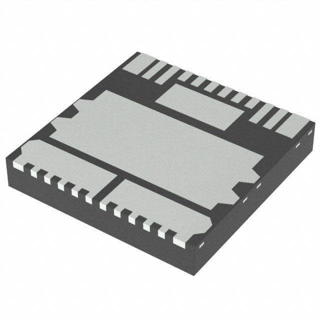
The 34984 is packaged in a power-enhanced 12 x 12 mm nonleaded PQFN
package with exposed tabs and powered by SMARTMOS technology.
HIGH-SIDE SWITCH
BOTTOM VIEW
FK SUFFIX
98ARL10521D
16-PIN PQFN
Features
•
•
•
•
Dual 4.0 m max. high-side switch with parallel input or SPI control
6.0 V to 27 V operating voltage with standby currents < 5.0 A
Output current monitoring with two SPI-selectable current ratios
SPI control of overcurrent limit, overcurrent fault blanking time, output OFF
open load detection, output ON/OFF control, watchdog timeout, slew-rates,
and fault status reporting
• SPI status reporting of overcurrent, open and shorted loads,
overtemperature, undervoltage and overvoltage shutdown, fail-safe pin
status, and program status
• Enhanced -16 V reverse polarity VPWR protection
VDD
VDD
Applications
•
•
•
•
VDD
Low-voltage factory automation
DC motor or solenoid
Resistive and inductive loads
Low-voltage industrial lighting
VPWR
34984
VDD
I/O
FS
I/O
WAKE
SO
SI
SCLK
MCU
GND
HS1
SCLK
CS
CS
SI
SO
I/O
RST
I/O
INO
I/O
IN1
A/D
VPWR
HS0
LOAD
CSNS
FSI
GND
Figure 1. 34984 Simplified Application Diagram
* This document contains certain information on a new product.
Specifications and information herein are subject to change without notice.
© Freescale Semiconductor, Inc., 2014. All rights reserved.
LOAD
�ORDERABLE PARTS
ORDERABLE PARTS
Table 1. Orderable Part Variations
Temperature Range (TA)
Part Number
MC34984CHFK(1)
-40 °C to 125 °C
Package
16 PQFN
Notes
1. To order parts in Tape & Reel, add the R2 suffix to the part number.
34984
2
Analog Integrated Circuit Device Data
Freescale Semiconductor
�INTERNAL BLOCK DIAGRAM
INTERNAL BLOCK DIAGRAM
VPWR
VDD
Internal
Regulator
IUP
VIC
Overvoltage
Protection
CS
Programmable
Switch Delay
0 –525 ms
SO
SPI
3.0 MHz
Selectable Slew
Rate Gate Drive
HS0
Selectable Overcurrent
High Detection
100A or 75A
SI
SCLK
FS
IN[0:1]
RST
WAKE
Logic
Selectable Overcurrent
Low Detection
Blanking Time
0.15–155 ms
Selectable Overcurrent
Low Detection
7.5 –25 A
Open Load
Detection
IDWN
Overtemperature
Detection
RDWN
HS0
HS1
Programmable
Watchdog
310–2500 ms
HS1
VIC
IUP
Selectable
Output Current
Recopy
1/20500 or 1/41000
FSI
GND
CSNS
Figure 2. 34984 Simplified Internal Block Diagram
34984
Analog Integrated Circuit Device Data
Freescale Semiconductor
3
�PIN CONNECTIONS
PIN CONNECTIONS
4
3 2
CSNS
RST
WAKE
6 5
FS
FSI
7
IN0
CS
SI
SCLK
VDD
SO
IN1
12 11 10 9 8
1
13
GND
TRANSPARENT
TOP VIEW
14
VPWR
15
HS1
16
HS0
Figure 3. 34984 Pin Connections (Transparent Top View)
Functional descriptions of many of these pins can be found in the Functional Pin Description section beginning on page 16.
Table 2. Pin Definitions
Pin
Pin Name
Pin
Function
Formal Name
Definition
1
CSNS
Output
Output Current Monitoring
This pin is used to output a current proportional to the designated HS0-1 output.
2
WAKE
Input
Wake
3
RST
Input
Reset (Active Low)
4
IN0
Input
Direct Input 0
5
FS
Output
Fault Status (Active Low)
This is an open drain configured output requiring an external pull-up resistor to
VDD for fault reporting.
6
FSI
Input
Fail-safe Input
The value of the resistance connected between this pin and ground determines
the state of the outputs after a watchdog timeout occurs.
7
CS
Input
Chip Select (Active Low)
8
SCLK
Input
Serial Clock
This input pin is connected to the MCU providing the required bit shift clock for
SPI communication.
9
SI
Input
Serial Input
This is a command data input pin connected to the SPI Serial Data Output of the
MCU or to the SO pin of the previous device of a daisy chain of devices.
10
VDD
Input
Digital Drain Voltage
(Power)
11
SO
Output
Serial Output
This output pin is connected to the SPI serial data input pin of the MCU or to the
SI pin of the next device of a daisy chain of devices.
12
IN1
Input
Direct Input 1
This input pin is used to directly control the output HS1.
13
GND
Ground
Ground
14
VPWR
Input
Positive Power Supply
This pin is used to input a Logic [1] signal so as to enable the watchdog timer
function.
This input pin is used to initialize the device configuration and fault registers, as
well as place the device in a low current Sleep mode.
This input pin is used to directly control the output HS0.
This input pin is connected to a chip select output of a master microcontroller
(MCU).
This is an external voltage input pin used to supply power to the SPI circuit.
This pin is the ground for the logic and analog circuitry of the device.
This pin connects to the positive power supply and is the source input of
operational power for the device.
34984
4
Analog Integrated Circuit Device Data
Freescale Semiconductor
�PIN CONNECTIONS
Table 2. Pin Definitions (continued)
Pin
Pin Name
Pin
Function
Formal Name
15
HS1
Output
High-side Output 1
Protected 4.0 m high-side power output to the load.
16
HS0
Output
High-side Output 0
Protected 4.0 m high-side power output to the load.
Definition
34984
Analog Integrated Circuit Device Data
Freescale Semiconductor
5
�ELECTRICAL CHARACTERISTICS
MAXIMUM RATINGS
ELECTRICAL CHARACTERISTICS
MAXIMUM RATINGS
Table 3. Maximum Ratings
All voltages are with respect to ground unless otherwise noted.
Symbol
Rating
Value
Unit
Notes
Operating Voltage Range
Steady-state
-16 to 41
V
VDD
VDD Supply Voltage
-0.3 to 5.5
V
VIN[0:1], RST, FSI,
CSNS, SI, SCLK,
Input/Output Voltage
- 0.3 to 7.0
V
(2)
- 0.3 to VDD + 0.3
V
(2)
ELECTRICAL RATINGS
VPWR
CS, FS
VSO
SO Output Voltage
ICL(WAKE)
WAKE Input Clamp Current
2.5
mA
ICL(CSNS)
CSNS Input Clamp Current
10
mA
41
-15
V
30
A
(3)
0.75
0.5
J
(4)
V
(5)
VHS
Output Voltage
Positive
Negative
IHS[0:1]
Output Current
ECL[0:1]
Output Clamp Energy
34984B
34984C
VESD1
VESD3
ESD Voltage
Human Body Model (HBM)
Charge Device Model (CDM)
Corner Pins (1, 12, 15, 16)
All Other Pins (2, 11, 13, 14)
± 2000
±750
±500
Notes
2. Exceeding this voltage limit may cause permanent damage to the device.
3. Continuous high-side output current rating so long as maximum junction temperature is not exceeded. Calculation of maximum output current using
package thermal resistance is required.
4. Active clamp energy using single-pulse method (L = 16 mH, RL = 0,VPWR = 12 V, TJ = 150 °C).
5.
ESD1 testing is performed in accordance with the Human Body Model (HBM) (CZAP = 100 pF, RZAP = 1500 ESD3 testing is performed in
accordance with the Charge Device Model (CDM), Robotic (CZAP = 4.0 pF).
34984
6
Analog Integrated Circuit Device Data
Freescale Semiconductor
�ELECTRICAL CHARACTERISTICS
MAXIMUM RATINGS
Table 3. Maximum Ratings (continued)
All voltages are with respect to ground unless otherwise noted.
Symbol
Rating
Value
Unit
Notes
Operating Temperature
Ambient
Junction
- 40 to 125
- 40 to 150
C
TSTG
Storage Temperature
- 55 to 150
C
RJC
RJA
Thermal Resistance
Junction-to-Case
Junction-to-Ambient
很抱歉,暂时无法提供与“MC34984CHFK”相匹配的价格&库存,您可以联系我们找货
免费人工找货