56F8014
Data Sheet
Technical Data
56F8000
16-bit Digital Signal Controllers
MC56F8014
Rev. 11
05/2008
freescale.com
�Document Revision History
Version History
Description of Change
Rev 0
Initial release
Rev 1
Updates to Part 10, Specifications,
Table 10-1, added maximum clamp current, per pin
Table 10-11, clarified variation over temperature table and graph
Table 10-15, added LIN slave timing
Rev 2
Added alternate pins to Figure 11-1 and Table 11-1.
Rev 3
Corrected bit selects in Timer Channel 3 Input (TC3_INP) bit 9, Section 6.3.1.7, clarified
Section 1.4.1, and simplified notes in Table 10-9,
Rev 4
Added clarification on sync inputs in Section 1.4.1, added voltage difference specification to
Table 10-1 and Table 10-4, deleted formula for Ambient Operating Temperature in Table 10-4,
and a note for pin group 3, corrected Table 8-1, error in Port C peripheral function configuration,
updated notes in Table 10-9. Added RoHs and “pb-free” language to back cover.
Rev 5
Updates to Section 10
Table 10-5, corrected max values for ADC Input Current High and Low; corrected typ value for
pull-up disabled Digital Input Current Low (a)
Table 10-6, corrected typ and added max values for Standby > Stop and Powerdown modes
Table 10-7, corrected min value for Low-Voltage Interrupt for 3.3V
Table 10-11, corrected typ and max values and units for PLL lock time
Table 10-12, corrected typ values for Relaxation Oscillator output frequency and variation over
temperature (also increased temp range to 150 degreesC) and added variation over
temperature from 0—105 degreesC
Updated Figure 10-5
Table 10-19, updated max values for Integral Non-Linearity full input signal range, Negative
Differential Non-Linearity, ADC internal clock, Offset Voltage Internal Ref, Gain Error and Offset
Voltage External Ref; updated typ values for Negative Differential Non-Linearity, Offset Voltage
Internal Ref, Gain Error and Offset Voltage External Ref; added new min values and corrected
typ values for Signal-to-noise ratio, Total Harmonic Distortion, Spurious Free Dynamic Range,
Signal-to-noise plus distortion, Effective Number of Bits
Rev 6
Added details to Section 1. Clarified language in State During Reset column in Table 2-3;
corrected flash data retention temperature in Table 10-4; moved input current high/low
toTable 10-19 and location of footnotes in Table 10-5; reorganized Table 10-19; clarified title of
Figure 10-1.
Rev. 7
• In Table 10-4, added an entry for flash data retention with less than 100 program/erase
cycles (minimum 20 years).
• In Table 10-6, changed the device clock speed in STOP mode from 8MHz to 4MHz.
• In Table 10-12, changed the typical relaxation oscillator output frequency in Standby mode
from 400kHz to 200kHz.
Rev. 8
In Table 10-19, changed the maximum ADC internal clock frequency from 8MHz to 5.33MHz.
56F8014 Technical Data, Rev. 11
2
Freescale Semiconductor
�Document Revision History (Continued)
Version History
Description of Change
Rev. 9
Added the following note to the description of the TMS signal in Table 2-3:
Note: Always tie the TMS pin to VDD through a 2.2K resistor.
Rev. 10
• In Table 2-3, changed VCAP value from 4.7 μF to 2.2 μF.
• In Table 2-3, changed the input type for FAULT3 (was “Output”, is “Input”).
• In Table 2-3, changed the input type for FAULT2 (was “Input/Output”, is “Input”).
• Revised Section 7, Security Features.
• Added MC56F8014MFAE to Section 13, Ordering Information.
• Fixed miscellaneous errors.
Rev.11
• Updated temperature information in Table 10-1 and Table 10-4.
Please see http://www.freescale.com for the most current data sheet revision.
56F8014 Technical Data, Rev. 11
Freescale Semiconductor
3
�56F8014 General Description
• Up to 32 MIPS at 32MHz core frequency
• One Inter-Integrated Circuit (I2C) Port
• DSP and MCU functionality in a unified,
C-efficient architecture
• Computer Operating Properly (COP)/Watchdog
• On-Chip Relaxation Oscillator
• 16KB Program Flash
• Integrated Power-On Reset and Low-Voltage Interrupt
Module
• 4KB Unified Data/Program RAM
• One 5-channel PWM module
• JTAG/Enhanced On-Chip Emulation (OnCE™) for
unobtrusive, real-time debugging
• Two 4-channel 12-bit ADCs
• Up to 26 GPIO lines
• One Serial Communication Interface (SCI) with LIN
slave functionality
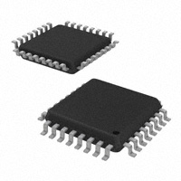
• 32-pin LQFP Package
• One Serial Peripheral Interface (SPI)
• One 16-bit Quad Timer
VCAP
RESET
VDD
4
5
PWM Outputs
JTAG/EOnCE
Port or
GPIOD
PWM
or Timer Port
or GPIOA
4
AD0
4
AD1
VDDA
VSSA
2
Digital Reg
Analog Reg
Low-Voltage
Supervisor
16-Bit
56800E Core
Address
Generation Unit
Program Controller
and Hardware
Looping Unit
VSS_IO
Data ALU
16 x 16 + 36 -> 36-Bit MAC
Three 16-bit Input Registers
Four 36-bit Accumulators
Bit
Manipulation
Unit
PAB
PDB
CDBR
CDBW
ADC
or
GPIOC
Memory
Program Memory
8K x 16 Flash
R/W Control
XDB2
XAB1
XAB2
System Bus
Control
PAB
Unified Data /
Program RAM
4KB
PDB
CDBR
CDBW
IPBus Bridge (IPBB)
2
Timer or
GPIOB
SPI or I2C
or Timer
or GPIOB
4
SCI
or I2C
or GPIOB
COP/
Watchdog
Interrupt
Controller
2
System
Integration
Module
P
O
R
O
Clock
S
Generator* C
*Includes On-Chip
Relaxation Oscillator
56F8014 Block Diagram
56F8014 Technical Data, Rev. 11
4
Freescale Semiconductor
�56F8014 Data Sheet Table of Contents
Part 1: Overview . . . . . . . . . . . . . . . . . . . . . . . 6
1.1.
1.2.
1.3.
1.4.
1.5.
1.6.
1.7.
1.8.
56F8014 Features . . . . . . . . . . . . . . . . . . . . 6
56F8014 Description. . . . . . . . . . . . . . . . . . . 8
Award-Winning Development Environment . 8
Architecture Block Diagram . . . . . . . . . . . . . 9
Synchronize ADC with PWM . . . . . . . . . . . . 9
Multiple Frequency PWM Output . . . . . . . . . 9
Product Documentation . . . . . . . . . . . . . . . 13
Data Sheet Conventions. . . . . . . . . . . . . . . 13
Part 2: Signal/Connection Descriptions . . . 14
Part 7: Security Features . . . . . . . . . . . . . . .82
7.1. Operation with Security Enabled . . . . . . . . . 82
7.2. Flash Access Lock and Unlock Mechanisms 83
7.3. Product Analysis. . . . . . . . . . . . . . . . . . . . . . 84
Part 8: General Purpose Input/Output (GPIO)
. . . . . . . . . . . . . . . . . . . . . . . . . . . . . . .84
8.1. Introduction. . . . . . . . . . . . . . . . . . . . . . . . . . 84
8.2. Configuration . . . . . . . . . . . . . . . . . . . . . . . . 84
8.3. Reset Values . . . . . . . . . . . . . . . . . . . . . . . . 86
2.1. Introduction . . . . . . . . . . . . . . . . . . . . . . . . . 14
2.2. 56F8014 Signal Pins . . . . . . . . . . . . . . . . . 18
Part 9: Joint Test Action Group (JTAG) . . .91
Part 3: OCCS . . . . . . . . . . . . . . . . . . . . . . . . . 26
Part 10: Specifications . . . . . . . . . . . . . . . . .91
3.1.
3.2.
3.3.
3.4.
3.5.
Overview. . . . . . . . . . . . . . . . . . . . . . . . . . .
Features . . . . . . . . . . . . . . . . . . . . . . . . . . .
Operating Modes . . . . . . . . . . . . . . . . . . . .
Block Diagram . . . . . . . . . . . . . . . . . . . . . .
Pin Descriptions . . . . . . . . . . . . . . . . . . . . .
26
26
26
28
29
Part 4: Memory Map . . . . . . . . . . . . . . . . . . . 29
4.1.
4.2.
4.3.
4.4.
4.5.
4.6.
Introduction . . . . . . . . . . . . . . . . . . . . . . . . .
Interrupt Vector Table . . . . . . . . . . . . . . . . .
Program Map . . . . . . . . . . . . . . . . . . . . . . .
Data Map . . . . . . . . . . . . . . . . . . . . . . . . . .
EOnCE Memory Map . . . . . . . . . . . . . . . . .
Peripheral Memory Mapped Registers . . . .
29
29
31
32
32
33
Part 5: Interrupt Controller (ITCN) . . . . . . . . 43
5.1.
5.2.
5.3.
5.4.
5.5.
5.6.
Introduction . . . . . . . . . . . . . . . . . . . . . . . . .
Features . . . . . . . . . . . . . . . . . . . . . . . . . . .
Functional Description . . . . . . . . . . . . . . . .
Block Diagram . . . . . . . . . . . . . . . . . . . . . .
Register Descriptions . . . . . . . . . . . . . . . . .
Resets . . . . . . . . . . . . . . . . . . . . . . . . . . . .
43
43
43
45
45
61
Part 6: System Integration Module (SIM) . . 62
6.1.
6.2.
6.3.
6.4.
6.5.
6.6.
6.7.
6.8.
Introduction . . . . . . . . . . . . . . . . . . . . . . . . .
Features . . . . . . . . . . . . . . . . . . . . . . . . . . .
Register Descriptions . . . . . . . . . . . . . . . . .
Clock Generation Overview . . . . . . . . . . . .
Power-Down Modes . . . . . . . . . . . . . . . . . .
Resets . . . . . . . . . . . . . . . . . . . . . . . . . . . .
Clocks . . . . . . . . . . . . . . . . . . . . . . . . . . . . .
Interrupts . . . . . . . . . . . . . . . . . . . . . . . . . .
62
62
64
77
77
79
81
82
9.1. 56F8014 Information . . . . . . . . . . . . . . . . . . 91
10.1. General Characteristics . . . . . . . . . . . . . . . 91
10.2. DC Electrical Characteristics . . . . . . . . . . . 95
10.3. AC Electrical Characteristics . . . . . . . . . . . 97
10.4. Flash Memory Characteristics . . . . . . . . . . 98
10.5. External Clock Operation Timing . . . . . . . . 99
10.6. Phase Locked Loop Timing . . . . . . . . . . . . 99
10.7. Relaxation Oscillator Timing. . . . . . . . . . . 100
10.8. Reset, Stop, Wait, Mode Select, and
Interrupt Timing . . . . . . . . . . . . . . 101
10.9. Serial Peripheral Interface (SPI) Timing . . 102
10.10. Quad Timer Timing. . . . . . . . . . . . . . . . . 105
10.11. Serial Communication Interface (SCI)
Timing . . . . . . . . . . . . . . . . . . . . . 107
10.12. Inter-Integrated Circuit Interface (I2C)
Timing . . . . . . . . . . . . . . . . . . . . . 108
10.13. JTAG Timing. . . . . . . . . . . . . . . . . . . . . . 109
10.14. Analog-to-Digital Converter (ADC)
Parameters . . . . . . . . . . . . . . . . . 111
10.15. Equivalent Circuit for ADC Inputs . . . . . . 112
10.16. Power Consumption . . . . . . . . . . . . . . . . 112
Part 11: Packaging . . . . . . . . . . . . . . . . . . .115
11.1. 56F8014 Package and Pin-Out
Information . . . . . . . . . . . . . . . . . . 115
Part 12: Design Considerations . . . . . . . . .118
12.1. Thermal Design Considerations . . . . . . . . 118
12.2. Electrical Design Considerations . . . . . . . 119
Part 13: Ordering Information . . . . . . . . . .121
Part 14: Appendix . . . . . . . . . . . . . . . . . . . .122
56F8014 Technical Data, Rev. 11
Freescale Semiconductor
5
�Part 1 Overview
1.1 56F8014 Features
1.1.1
•
•
•
•
•
•
•
•
•
•
•
•
•
•
1.1.2
Digital Signal Controller Core
Efficient 16-bit 56800E family Digital Signal Controller (DSC) engine with dual Harvard architecture
As many as 32 Million Instructions Per Second (MIPS) at 32MHz core frequency
Single-cycle 16 × 16-bit parallel Multiplier-Accumulator (MAC)
Four 36-bit accumulators, including extension bits
32-bit arithmetic and logic multi-bit shifter
Parallel instruction set with unique DSP addressing modes
Hardware DO and REP loops
Three internal address buses
Four internal data buses
Instruction set supports both DSP and controller functions
Controller-style addressing modes and instructions for compact code
Efficient C compiler and local variable support
Software subroutine and interrupt stack with depth limited only by memory
JTAG/Enhanced On-Chip Emulation (OnCE) for unobtrusive, processor speed-independent, real-time
debugging
Memory
•
Dual Harvard architecture permits as many as three simultaneous accesses to program and data memory
•
•
Flash security and protection that prevent unauthorized users from gaining access to the internal Flash
On-chip memory
— 16KB of Program Flash
— 4KB of Unified Data/Program RAM
•
1.1.3
•
EEPROM emulation capability using Flash
Peripheral Circuits for 56F8014
One multi-function five-output Pulse Width Modulator (PWM) module
— Up to 96MHz PWM operating clock
— 15 bits of resolution
— Center-aligned and Edge-aligned PWM signal mode
— Three programmable fault inputs with programmable digital filter
— Double-buffered PWM registers
56F8014 Technical Data, Rev. 11
6
Freescale Semiconductor
�56F8014 Features
•
•
•
•
•
•
•
•
•
•
— Each complementary PWM signal pair can output a different switching frequency by selecting
PWM generation sources from:
– PWM generator
– External GPIO
– Internal timers
– ADC conversion result of over/under limits:
When conversion result is greater than high limit, deactivate PWM signal
When conversion result is less than low limit, activate PWM signal
Two independent 12-bit Analog-to-Digital Converters (ADCs)
— 2 x 4 channel inputs
— Supports both simultaneous and sequential conversions
— ADC conversions can be synchronized by both PWM and timer modules
— Sampling rate up to 2.67MSPS
— 8-word result buffer registers
— ADC Smart Power Management (Auto-standby, auto-powerdown)
One 16-bit multi-purpose Quad Timer module (TMR)
— Up to 96MHz operating clock
— Four independent 16-bit counter/timers with cascading capability
— Each timer has capture and compare capability
— Up to 12 operating modes
One Serial Communication Interface (SCI) with LIN slave functionality
— Full-duplex or single-wire operation
— Two receiver wake-up methods:
– Idle line
– Address mark
One Serial Peripheral Interface (SPI)
— Full-duplex operation
— Master and slave modes
— Programmable length transactions (two to sixteen bits)
One Inter-Integrated Circuit (I2C) port
— Operates up to 400 kbps
— Supports both master and slave operation
Computer Operating Properly (COP)/Watchdog timer capable of selecting different clock sources
Up to 26 General-Purpose I/O (GPIO) pins with 5V tolerance
Integrated Power-On Reset and Low-Voltage Interrupt Module
Phase Lock Loop (PLL) provides a high-speed clock to the core and peripherals
Clock Sources:
— On-chip relaxation oscillator
56F8014 Technical Data, Rev. 11
Freescale Semiconductor
7
�•
•
1.1.4
•
•
•
•
•
— External clock source
On-chip regulators for digital and analog circuitry to lower cost and reduce noise
JTAG/EOnCE debug programming interface for real-time debugging
Energy Information
Fabricated in high-density CMOS with 5V-tolerant, TTL-compatible digital inputs
On-chip regulators for digital and analog circuitry to lower cost and reduce noise
Wait and Stop modes available
ADC smart power management
Each peripheral can be individually disabled to save power
1.2 56F8014 Description
The 56F8014 is a member of the 56800E core-based family of Digital Signal Controllers (DSCs). It
combines, on a single chip, the processing power of a DSP and the functionality of a microcontroller with
a flexible set of peripherals to create an extremely cost-effective solution. Because of its low cost,
configuration flexibility, and compact program code, the 56F8014 is well-suited for many applications.
The 56F8014 includes many peripherals that are especially useful for industrial control, motion control,
home appliances, general purpose inverters, smart sensors, fire and security systems, switched-mode
power supplies, power management, and medical monitoring applications.
The 56800E core is based on a dual Harvard-style architecture consisting of three execution units
operating in parallel, allowing as many as six operations per instruction cycle. The MCU-style
programming model and optimized instruction set allow straightforward generation of efficient, compact
DSP and control code. The instruction set is also highly efficient for C compilers to enable rapid
development of optimized control applications.
The 56F8014 supports program execution from internal memories. Two data operands can be accessed
from the on-chip data RAM per instruction cycle. The 56F8014 also offers up to 26 General Purpose
Input/Output (GPIO) lines, depending on peripheral configuration.
The 56F8014 Digital Signal Controller includes 16KB of Program Flash and 4KB of Unified
Data/Program RAM. Program Flash memory can be independently bulk erased or erased in pages.
Program Flash page erase size is 512 Bytes/256 Words.
A full set of programmable peripherals—PWM, ADCs, SCI, SPI, I2C, Quad Timer—support various
applications. Each peripheral can be independently shut down to save power. Any pin in these peripherals
can also be used as a General Purpose Input/Outputs (GPIO).
1.3 Award-Winning Development Environment
Processor ExpertTM (PE) provides a Rapid Application Design (RAD) tool that combines easy-to-use
component-based software application creation with an expert knowledge system.
The CodeWarrior Integrated Development Environment is a sophisticated tool for code navigation,
compiling, and debugging. A complete set of evaluation modules (EVMs), demonstration board kit and
development system cards will support concurrent engineering. Together, PE, CodeWarrior and EVMs
56F8014 Technical Data, Rev. 11
8
Freescale Semiconductor
�Architecture Block Diagram
create a complete, scalable tools solution for easy, fast, and efficient development.
1.4 Architecture Block Diagram
The 56F8014’s architecture is shown in Figure 1-1, Figure 1-2, and Figure 1-3. Figure 1-1 illustrates
how the 56800E system buses communicate with internal memories and the IPBus Bridge, as well as
showing the internal connections between each unit of the 56800E core. Figure 1-2 shows the peripherals
and control blocks connected to the IPBus Bridge. Figure 1-3 details how the device’s I/O pins are muxed.
The figures do not show the on-board regulator and power and ground signals. They also do not show the
multiplexing between peripherals or the dedicated GPIOs. Please see Part 2 Signal/Connection
Descriptions to see which signals are multiplexed with those of other peripherals.
1.5 Synchronize ADC with PWM
ADC conversion can be synchronized with the PWM module via Quad Timer channel 2 and 3 if needed.
Internally, the PWM synch signal — which is generated at every PWM reload —can be connected to the
timer channel 3 input, and the timer channel 2 and channel 3 outputs are connected to the ADC sync inputs.
Timer channel 3 output is connected to SYNC0 and timer channel 2 is connected to SYNC1. The setting
is controlled by the TC3_INP bit in the SIM Control Register; see Section 6.3.1.
SYNC0 is the master ADC sync input, used to trigger both ADCA and ADCB in sequence and parallel
mode. SYNC1 is used to trigger ADCB in parallel independent mode, while SYNC0 is used to trigger
ADCA. See MC56F8000RM, the 56F801X Peripheral Reference Manual, for additional information.
1.6 Multiple Frequency PWM Output
When both PWM channels of a complementary pair in software control mode and software control bits
are set to 1, each complementary PWM signal pair — PWM 0 and 1; PWM 2 and 3; and PWM 4 and 5 —
can select a PWM source from one of the following sources. This will enable each PWM pair and PWM2
to output PWM signals at different frequencies.
•
•
•
External GPIO input:
— GPIOB2 input can be used to drive PWM 0 and 1
— GPIOB3 input can be used to drive PWM 2
— GPIOB4 input can be used to drive PWM 4 and 5
Quad Timer output:
— Timer0 output can be used to drive PWM 0 and 1
— Timer2 output can be used to drive PWM 2
— Timer3 output can be used to drive PWM 4 and 5
ADC conversion result:
— Signal of over/under limit of ADC sample 0 can be used to drive PWM 0 and 1
— Signal of over/under limit of ADC sample 1 can be used to drive PWM 2
56F8014 Technical Data, Rev. 11
Freescale Semiconductor
9
�— Signal of over/under limit of ADC sample 2 can be used to drive PWM 4 and 5
DSP56800E Core
Program Control Unit
PC
LA
LA2
HWS0
HWS1
FIRA
OMR
SR
LC
LC2
FISR
Address
Generation
Unit
(AGU)
Instruction
Decoder
Interrupt
Unit
ALU1
ALU2
R0
R1
R2
R3
R4
R5
N
M01
N3
Looping
Unit
Program
Memory
SP
XAB1
XAB2
PAB
PDB
Data /
Program
RAM
CDBW
CDBR
XDB2
A2
B2
C2
D2
BitManipulation
Unit
Enhanced
OnCE™
JTAG TAP
Y
A1
B1
C1
D1
Y1
Y0
X0
MAC and ALU
A0
B0
C0
D0
IPBUS
Interface
Data
Arithmetic
Logic Unit
(ALU)
Multi-Bit Shifter
Figure 1-1 56800E Core Block Diagram
56F8014 Technical Data, Rev. 11
10
Freescale Semiconductor
�Multiple Frequency PWM Output
To/From IPBus Bridge
CLKGEN
(ROSC / PLL /
CLKIN)
GPIOAn
GPIOBn
8
8
GPIOCn
6
GPIODn
4
Interrupt
Controller
Low-Voltage Interrupt
GPIO A
POR & LVI
GPIO B
System POR
GPIO C
SIM
RESET / GPIOA7
GPIO D
COP Reset
COP
IPBus
(Continues on Figure 1-3)
Figure 1-2 Peripheral Subsystem
56F8014 Technical Data, Rev. 11
Freescale Semiconductor
11
�(Continued from Figure 1-2)
To/From IPBus Bridge
2
PWM4, 5
PWM
PWM0 - 3
4
PWM0 - 3
GPIOA0 - 3
2
Fault1, 2
PWM4, 5
Fault0
Output Controls
Reload
Pulse
3
Fault1, 2
Fault3
T2, 3
2
2
Fault0
from ADC
T3i
GPIOA4 - 5
GPIOA6
Fault3
T2/3
2
T1
GPIOB5
T1
Timer
T2o, T3o
T0
T0
I2C is muxed with both SPI and SCI.
T2 and T3 are muxed with SPI and PWM.
CLKO
GPIOB4
2
2
SCI
I2C
SPI
3
TXD, RXD
2
SDA, SCL
2
SCLK, SS
2
MISO, MOSI
2
GPIOB6 - 7
GPIOB0 - 1
T2, 3
to PWM
GPIOB2 - 3
Sync0,
Sync1
Over/Under
Limits
ADC
ANA0, 1, 3
3
ANA0, 1, 3
ANA2
ANA2
VREFH, VREFL
ANB2
ANB0, 1, 3
GPIOC0, 1, 3
ANB2
2
VREFH, VREFL
GPIOC2, 6
3
ANB0, 1, 3
GPIOC4, 5, 7
IPBus
Figure 1-3 56F8014 Peripheral I/O Pin-Out
56F8014 Technical Data, Rev. 11
12
Freescale Semiconductor
�Product Documentation
1.7 Product Documentation
The documents listed in Table 1-1 are required for a complete description and proper design with the
56F8014. Documentation is available from local Freescale distributors, Freescale Semiconductor sales offices,
Freescale Literature Distribution Centers, or online at:
http://www.freescale.com
Table 1-1 56F8014 Chip Documentation
Topic
Description
Order Number
DSP56800E
Reference Manual
Detailed description of the 56800E family architecture,
16-bit Digital Signal Controller core processor, and the
instruction set
DSP56800ERM
56F801X Peripheral
Reference Manual
Detailed description of peripherals of the 56F801X
family of devices
MC56F8000RM
56F801x Serial
Bootloader User Guide
Detailed description of the Serial Bootloader in the
56F801x family of devices
56F801xBLUG
56F8014
Technical Data Sheet
Electrical and timing specifications, pin descriptions,
and package descriptions (this document)
MC56F8014
56F8014
Errata
Details any chip issues that might be present
MC56F8014E
1.8 Data Sheet Conventions
This data sheet uses the following conventions:
OVERBAR
This is used to indicate a signal that is active when pulled low. For example, the RESET pin is
active when low.
“asserted”
A high true (active high) signal is high or a low true (active low) signal is low.
“deasserted”
A high true (active high) signal is low or a low true (active low) signal is high.
Examples:
Signal/Symbol
Logic State
Signal State
Voltage1
PIN
True
Asserted
VIL/VOL
PIN
False
Deasserted
VIH/VOH
PIN
True
Asserted
VIH/VOH
PIN
False
Deasserted
VIL/VOL
1. Values for VIL, VOL, VIH, and VOH are defined by individual product specifications.
56F8014 Technical Data, Rev. 11
Freescale Semiconductor
13
�Part 2 Signal/Connection Descriptions
2.1 Introduction
The input and output signals of the 56F8014 are organized into functional groups, as detailed in
Table 2-1. Table 2-2 summarizes all device pins. In Table 2-2, each table row describes the signal or
signals present on a pin, sorted by pin number.
Table 2-1 Functional Group Pin Allocations
Functional Group
Number of Pins
Power (VDD or VDDA)
2
Ground (VSS or VSSA)
3
Supply Capacitors
1
Reset
1
Pulse Width Modulator (PWM) Ports1
5
Serial Peripheral Interface (SPI) Ports2
4
Analog-to-Digital Converter (ADC) Ports
8
Timer Module Ports3
2
Serial Communications Interface (SCI) Ports4
2
JTAG/Enhanced On-Chip Emulation (EOnCE)
4
1. Pins in this section can function as TMR and GPIO.
2. Pins in this section can function as TMR, I2C, and GPIO.
3. Pins can function as PWM and GPIO.
4. Pins in this section can function as I2C and GPIO.
56F8014 Technical Data, Rev. 11
14
Freescale Semiconductor
�Introduction
Table 2-2 56F8014 Pins
Peripherals:
LQFP
Pin #
Pin
Name
Signal Name
GPIO I2C
SCI
SPI
ADC
PWM
Quad Power &
Timer Ground
1
GPIOB1 GPIOB1, SS,
SDA
B1
SDA
2
GPIOB7 GPIOB7, TXD,
SCL
B7
SCL
3
GPIOB5 GPIOB5, T1,
FAULT3
B5
4
ANB0
ANB0, GPIOC4
C4
ANB0
5
ANB1
ANB1, GPIOC5
C5
ANB1
6
ANB2
ANB2, VREFL,
GPIOC6
C6
ANB2,
VREFL
7
ANB3
ANB3, GPIOC7
C7
ANB3
8
VDDA
VDDA
VDDA
9
VSSA
VSSA
VSSA
10
ANA3
ANA3, GPIOC3
C3
ANA3
11
ANA2
ANA2, VREFH,
GPIOC2
C2
ANA2,
VREFH
12
ANA1
ANA1, GPIOC1
C1
ANA1
13
ANA0
ANA0, GPIOC0
C0
ANA0
14
VSS_IO
VSS_IO
15
TCK
TCK, GPIOD2
D2
16
RESET
RESET, GPIOA7
A7
17
GPIOB3 GPIOB3, MOSI,
T3
B3
MOSI
T3
18
GPIOB2 GPIOB2, MISO,
T2
B2
MISO
T2
19
GPIOB4 GPIOB4, T0,
CLKO
B4
20
GPIOA5 GPIOA5, PWM5,
FAULT2, T3
A5
21
GPIOB0 GPIOB0, SCLK,
SCL
B0
22
GPIOA4 GPIOA4, PWM4,
FAULT1, T2
23
GPIOA2 GPIOA2, PWM2
24
VCAP
JTAG
Misc.
SS
TXD
FAULT3
T1
VSS_IO
TCK
RESET
T0
PWM5,
FAULT2
T3
A4
PWM4,
FAULT1
T2
A2
PWM2
SCL
CLKO
SCLK
VCAP
VCAP
56F8014 Technical Data, Rev. 11
Freescale Semiconductor
15
�Table 2-2 56F8014 Pins (Continued)
Peripherals:
LQFP
Pin #
Pin
Name
Signal Name
GPIO I2C
SCI
SPI
ADC
PWM
Quad Power &
Timer Ground
JTAG
25
VDD_IO VDD_IO
VDD_IO
26
VSS_IO
VSS_IO
27
GPIOA1 GPIOA1, PWM1
A1
PWM1
28
GPIOA0 GPIOA0, PWM0
A0
PWM0
29
TDI
TDI, GPIOD0
D0
TDI
30
TMS
TMS, GPIOD3
D3
TMS
31
TDO
TDO, GPIOD1
D1
TDO
32
GPIOB6 GPIOB6, RXD,
SDA, CLKIN
B6
VSS_IO
SDA
RXD
Misc.
CLKIN
56F8014 Technical Data, Rev. 11
16
Freescale Semiconductor
�Introduction
VDD_IO
Power
VSS_IO
Ground
VDDA
Power
VSSA
Ground
1
2
1
1
56F8014
Other
Supply
Ports
VCAP
1
GPIOB0 (SCLK, SCL)
GPIOB1 (SS, SDA)
1
1
GPIOB2 (MISO, T2)
SPI Port or
I2C Port or
Timer Port
or GPIO
1
GPIOB3 (MOSI, T3)
1
SCI Port or
I2C Port or
GPIO
GPIOB6 (RXD, SDA, CLKIN)
1
GPIOB7 (TXD, SCL)
GPIOA0 - 2 (PWM0 - 2)
3
1
GPIOA4 (PWM4, FAULT1, T2)
1
PWM Port or
Timer Port or
GPIO
GPIOA5 (PWM5, FAULT2, T3)
RESET
1
RESET (GPIOA7)
1
2
GPIOB4 (T0, CLKO)
Timer Port
or GPIO
1
1
ANA0 - 1 (GPIOC0 - 1)
ANA2 (VREFH, GPIOC2)
ANA3 (GPIOC3)
1
GPIOB5 (T1, FAULT3)
1
ANB0 - 1 (GPIOC4 - 5)
ADC Port or
GPIO
2
1
ANB2 (VREFL, GPIOC6)
ANB3 (GPIOC7)
1
TCK (GPIOD2)
1
JTAG/
EOnCE Port
or GPIO
TMS (GPIOD3)
1
TDI (GPIOD0)
1
TDO (GPIOD1)
1
Figure 2-1 56F8014 Signals Identified by Functional Group (32-Pin LQFP)
56F8014 Technical Data, Rev. 11
Freescale Semiconductor
17
�2.2 56F8014 Signal Pins
After reset, each pin is configured for its primary function (listed first). Any alternate functionality must
be programmed.
Table 2-3 56F8014 Signal and Package Information for the 32-Pin LQFP
Signal
Name
LQFP
Pin No.
Type
State During
Reset
Signal Description
VDD_IO
25
Supply
Supply
I/O Power — This pin supplies 3.3V power to the chip I/O interface.
VSS_IO
14
Supply
Supply
VSS — These pins provide ground for chip logic and I/O drivers.
VSS_IO
26
VDDA
8
Supply
Supply
ADC Power — This pin supplies 3.3V power to the ADC modules. It
must be connected to a clean analog power supply.
VSSA
9
Supply
Supply
ADC Analog Ground — This pin supplies an analog ground to the
ADC modules.
VCAP
24
Supply
Supply
VCAP — Connect a 2.2 μF or greater bypass capacitor between this
pin and VSS_IO, which is required by the internal voltage regulator
for proper chip operation. See Section 10.2.1.
GPIOB6
32
Input/
Output
Input with
internal
pull-up
enabled
Port B GPIO — This GPIO pin can be individually programmed as
an input or output pin.
(RXD)
Input
(SDA1)
Input/
Output
(CLKIN)
Input
Receive Data — SCI receive data input.
Serial Data — This pin serves as the I2C serial data line.
Clock Input — This pin serves as an optional external clock input.
After reset, the default state is GPIOB6. The alternative peripheral
functionality is controlled via the SIM (See Section 6.3.8) and the
CLKMODE bit of the OCCS Oscillator Control Register.
1. This signal is also brought out on the GPIOB1 pin.
Return to Table 2-2
56F8014 Technical Data, Rev. 11
18
Freescale Semiconductor
�56F8014 Signal Pins
Table 2-3 56F8014 Signal and Package Information for the 32-Pin LQFP (Continued)
Signal
Name
LQFP
Pin No.
GPIOB7
2
Type
Input/
Output
State During
Reset
Input with
internal
pull-up
enabled
Signal Description
Port B GPIO — This GPIO pin can be individually programmed as
an input or output pin.
(TXD)
Input/
Output
Transmit Data — SCI transmit data output or transmit / receive in
single wire opeation.
(SCL2)
Input/
Output
Serial Clock — This pin serves as the I2C serial clock.
After reset, the default state is GPIOB7. The alternative peripheral
functionality is controlled via the SIM. See Section 6.3.8.
2. This signal is also brought out on the GPIOB0 pin.
RESET
16
(GPIOA7)
Input
Input with
internal
pull-up
enabled
Input/Open
Drain
Output
Reset — This input is a direct hardware reset on the processor.
When RESET is asserted low, the chip is initialized and placed in the
reset state. A Schmitt trigger input is used for noise immunity. The
internal reset signal will be deasserted synchronous with the internal
clocks after a fixed number of internal clocks.
Port A GPIO — This GPIO pin can be individually programmed as
an input or open drain output pin. Note that RESET functionality is
disabled in this mode and the chip can only be reset via POR, COP
reset, or software reset.
After reset, the default state is RESET.
GPIOB4
19
Input/
Output
Input with
internal
pull-up
enabled
Port B GPIO — This GPIO pin can be individually programmed as
an input or output pin.
(T0)
Input/
Output
T0 — Timer, Channel 0
(CLKO)
Output
Clock Output — This is a buffered clock signal. Using the
SIM_CLKO Select Register (SIM_CLKOSR), this pin can be
programmed as any of the following: disabled (logic 0), CLK_MSTR
(system clock), IPBus clock, or oscillator output. See Section 6.3.7.
After reset, the default state is GPIOB4. The alternative peripheral
functionality is controlled via the SIM. See Section 6.3.8.
Return to Table 2-2
56F8014 Technical Data, Rev. 11
Freescale Semiconductor
19
�Table 2-3 56F8014 Signal and Package Information for the 32-Pin LQFP (Continued)
Signal
Name
LQFP
Pin No.
GPIOB5
3
Type
Input/
Output
(T1)
Input/
Output
(FAULT3)
Input
State During
Reset
Input with
internal
pull-up
enabled
Signal Description
Port B GPIO — This GPIO pin can be individually programmed as
an input or output pin.
T1 — Timer, Channel 1
FAULT3 — This fault input pin is used for disabling selected PWM
outputs in cases where fault conditions originate off-chip.
After reset, the default state is GPIOB5. The alternative peripheral
functionality is controlled via the SIM. See Section 6.3.8.
TCK
15
(GPIOD2)
Input
Input with
internal
pull-up
enabled
Input/
Output
Test Clock Input — This input pin provides a gated clock to
synchronize the test logic and shift serial data to the JTAG/EOnCE
port. The pin is connected internally to a pull-up resistor. A Schmitt
trigger input is used for noise immunity.
Port D GPIO — This GPIO pin can be individually programmed as
an input or output pin.
After reset, the default state is TCK.
TMS
30
(GPIOD3)
Input
Input with
internal
pull-up
enabled
Input/
Output
Test Mode Select Input — This input pin is used to sequence the
JTAG TAP controller’s state machine. It is sampled on the rising
edge of TCK and has an on-chip pull-up resistor.
Port D GPIO — This GPIO pin can be individually programmed as
an input or output pin.
After reset, the default state is TMS.
Note: Always tie the TMS pin to VDD through a 2.2K resistor if this pin
is configured as TMS.
TDI
29
(GPIOD0)
Input
Input/
Output
Input with
internal
pull-up
enabled
Test Data Input — This input pin provides a serial input data stream
to the JTAG/EOnCE port. It is sampled on the rising edge of TCK
and has an on-chip pull-up resistor.
Port D GPIO — This GPIO pin can be individually programmed as
an input or output pin.
After reset, the default state is TDI.
Return to Table 2-2
56F8014 Technical Data, Rev. 11
20
Freescale Semiconductor
�56F8014 Signal Pins
Table 2-3 56F8014 Signal and Package Information for the 32-Pin LQFP (Continued)
Signal
Name
LQFP
Pin No.
Type
State During
Reset
TDO
31
Output
Output
(GPIOD1)
Input/
Output
Signal Description
Test Data Output — This tri-stateable output pin provides a serial
output data stream from the JTAG/EOnCE port. It is driven in the
shift-IR and shift-DR controller states, and changes on the falling
edge of TCK.
Port D GPIO — This GPIO pin can be individually programmed as
an input or output pin.
After reset, the default state is TDO.
GPIOB0
21
Input/
Output
Input with
internal
pull-up
enabled
Port B GPIO — This GPIO pin can be individually programmed as
an input or output pin.
(SCLK)
Input/
Output
SPI Serial Clock — In the master mode, this pin serves as an
output, clocking slaved listeners. In slave mode, this pin serves as
the data clock input. A Schmitt trigger input is used for noise
immunity.
(SCL3)
Input/
Output
Serial Data — This pin serves as the I2C serial clock.
After reset, the default state is GPIOB0. The alternative peripheral
functionality is controlled via the SIM. See Section 6.3.8.
3. This signal is also brought out on the GPIOB7 pin.
GPIOB1
1
Input/
Output
(SS)
Input
(SDA4)
Input/
Output
Input with
internal
pull-up
enabled
Port B GPIO — This GPIO pin can be individually programmed as
an input or output pin.
SPI Slave Select — SS is used in slave mode to indicate to the SPI
module that the current transfer is to be received.
Serial Clock — This pin serves as the I2C serial data line.
After reset, the default state is GPIOB1. The alternative peripheral
functionality is controlled via the SIM. See Section 6.3.8.
4. This signal is also brought out on the GPIOB6 pin.
Return to Table 2-2
56F8014 Technical Data, Rev. 11
Freescale Semiconductor
21
�Table 2-3 56F8014 Signal and Package Information for the 32-Pin LQFP (Continued)
Signal
Name
LQFP
Pin No.
GPIOB2
18
Type
Input/
Output
State During
Reset
Input with
internal
pull-up
enabled
Signal Description
Port B GPIO — This GPIO pin can be individually programmed as
an input or output pin.
(MISO)
Input/
Output
SPI Master In/Slave Out — This serial data pin is an input to a
master device and an output from a slave device. The MISO line of a
slave device is placed in the high-impedance state if the slave device
is not selected. The slave device places data on the MISO line a
half-cycle before the clock edge the master device uses to latch the
data.
(T25)
Input/
Output
T2 — Timer, Channel 2
After reset, the default state is GPIOB2. The alternative peripheral
functionality is controlled via the SIM. See Section 6.3.8.
5. This signal is also brought out on the GPIOA4 pin.
GPIOB3
17
Input/
Output
Input with
internal
pull-up
enabled
Port B GPIO — This GPIO pin can be individually programmed as
an input or output pin.
(MOSI)
Input/
Output
SPI Master Out/Slave In— This serial data pin is an output from a
master device and an input to a slave device. The master device
places data on the MOSI line a half-cycle before the clock edge the
slave device uses to latch the data.
(T36)
Input/
Output
T3 — Timer, Channel 3
After reset, the default state is GPIOB3. The alternative peripheral
functionality is controlled via the SIM. See Section 6.3.8.
6. This signal is also brought out on the GPIOA5 pin.
GPIOA0
28
(PWM0)
Input/
Output
Output
Input with
internal
pull-up
enabled
Port A GPIO — This GPIO pin can be individually programmed as
an input or output pin.
PWM0 — This is one of the six PWM output pins.
After reset, the default state is GPIOA0.
Return to Table 2-2
56F8014 Technical Data, Rev. 11
22
Freescale Semiconductor
�56F8014 Signal Pins
Table 2-3 56F8014 Signal and Package Information for the 32-Pin LQFP (Continued)
Signal
Name
LQFP
Pin No.
GPIOA1
27
(PWM1)
Type
Input/
Output
State During
Reset
Input with
internal
pull-up
enabled
Output
Signal Description
Port A GPIO — This GPIO pin can be individually programmed as
an input or output pin.
PWM1 — This is one of the six PWM output pins.
After reset, the default state is GPIOA1.
GPIOA2
23
(PWM2)
Input/
Output
Input with
internal
pull-up
enabled
Output
Port A GPIO — This GPIO pin can be individually programmed as
an input or output pin.
PWM2 — This is one of the six PWM output pins.
After reset, the default state is GPIOA2.
GPIOA4
22
Input/
Output
(PWM4)
Output
(FAULT1)
Input
(T27)
Input/
Output
Input with
internal
pull-up
enabled
Port A GPIO — This GPIO pin can be individually programmed as
an input or output pin.
PWM4 — This is one of the six PWM output pins.
Fault1 — This fault input pin is used for disabling selected PWM
outputs in cases where fault conditions originate off-chip.
T2 — Timer, Channel 2
After reset, the default state is GPIOA4. The alternative peripheral
functionality is controlled via the SIM. See Section 6.3.8.
7. This signal is also brought out on the GPIOB2 pin.
GPIOA5
20
Input/
Output
(PWM5)
Output
(FAULT2)
Input
(T38)
Input/
Output
Input with
internal
pull-up
enabled
Port A GPIO — This GPIO pin can be individually programmed as
an input or output pin.
PWM5 — This is one of the six PWM output pins.
Fault2 — This fault input pin is used for disabling selected PWM
outputs in cases where fault conditions originate off-chip.
T3 — Timer, Channel 3
After reset, the default state is GPIOA5. The alternative peripheral
functionality is controlled via the SIM. See Section 6.3.8.
8. This signal is also brought out on the GPIOB3 pin.
Return to Table 2-2
56F8014 Technical Data, Rev. 11
Freescale Semiconductor
23
�Table 2-3 56F8014 Signal and Package Information for the 32-Pin LQFP (Continued)
Signal
Name
LQFP
Pin No.
Type
ANA0
13
Input
(GPIOC0)
State During
Reset
Analog
Input
Input/
Output
Signal Description
ANA0 — Analog input to ADC A, channel 0
Port C GPIO — This GPIO pin can be individually programmed as
an input or output pin.
After reset, the default state is ANA0.
ANA1
12
(GPIOC1)
Input
Analog
Input
Input/
Output
ANA1 — Analog input to ADC A, channel 1
Port C GPIO — This GPIO pin can be individually programmed as
an input or output pin.
After reset, the default state is ANA1.
ANA2
11
Input
(VREFH)
Input
(GPIOC2)
Input/
Output
Analog
Input
ANA2 — Analog input to ADC A, channel 2
VREFH — Analog reference voltage high
Port C GPIO — This GPIO pin can be individually programmed as
an input or output pin.
After reset, the default state is ANA2.
ANA3
10
(GPIOC3)
Input
Analog
Input
Input/
Output
ANA3 — Analog input to ADC A, channel 3
Port C GPIO — This GPIO pin can be individually programmed as
an input or output pin.
After reset, the default state is ANA3.
ANB0
4
(GPIOC4)
Input
Input/
Output
Analog
Input
ANB0 — Analog input to ADC B, channel 0
Port C GPIO — This GPIO pin can be individually programmed as
an input or output pin.
After reset, the default state is ANB0.
Return to Table 2-2
56F8014 Technical Data, Rev. 11
24
Freescale Semiconductor
�56F8014 Signal Pins
Table 2-3 56F8014 Signal and Package Information for the 32-Pin LQFP (Continued)
Signal
Name
LQFP
Pin No.
Type
ANB1
5
Input
(GPIOC5)
State During
Reset
Analog
Input
Input/
Output
Signal Description
ANB1 — Analog input to ADC B, channel 1
Port C GPIO — This GPIO pin can be individually programmed as
an input or output pin.
After reset, the default state is ANB1.
ANB2
6
Input
(VREFL)
Input
(GPIOC6)
Input/
Output
Analog
Input
ANB2 — Analog input to ADC B, channel 2
VREFL — Analog reference voltage low. This should normally be
connected to a low-noise VSS.
Port C GPIO — This GPIO pin can be individually programmed as
an input or output pin.
After reset, the default state is ANB2.
ANB3
7
(GPIOC7)
Input
Input/
Output
Analog
Input
ANB3 — Analog input to ADC B, channel 3
Port C GPIO — This GPIO pin can be individually programmed as
an input or output pin.
After reset, the default state is ANB3.
Return to Table 2-2
56F8014 Technical Data, Rev. 11
Freescale Semiconductor
25
�Part 3 OCCS
3.1 Overview
This module provides the system clock, which uses it to generate the various chip clocks. This module also
produces the oscillator clock signals, plus the ADC clock and high-speed peripheral clock.
The on-chip clock synthesis module allows product design using an internal relaxation oscillator to run
56F801X family parts at user-selectable frequencies up to 32MHz.
3.2 Features
The On-Chip Clock Synthesis (OCCS) module interfaces to the oscillator and PLL. The OCCS module
features:
•
•
•
•
•
•
•
•
•
Internal relaxation oscillator
Ability to power down the internal relaxation oscillator
Ability to put the internal relaxation oscillator into a standby mode
3-bit postscaler provides control for the PLL output
Ability to power down the internal PLL
Provides 2X system clock frequency, which operates at twice the system clock, to the System Integration
Module (SIM) that is used to generate the various device clocks
Provides 3X system clock, which operates at three times the system clock, to PWM and Timer
Safety shutdown feature is available in the event that the PLL reference clock disappears
Can be driven from an external clock source
The clock generation module provides the programming interface for both the PLL and internal relaxation
oscillator.
3.3 Operating Modes
In 56F801X family parts, either an internal oscillator or an external frequency source can be used to
provide a reference clock to the SIM.
The 2X system clock source output from the OCCS can be described by one of the following equations:
2X system frequency = oscillator frequency
2X system frequency = (oscillator frequency X 8) / (postscaler)
where:
postscaler = 1, 2, 4, 8, 16, or 32 PLL output divider
The SIM is responsible for further dividing these frequencies by two, which will insure a 50% duty cycle
in the system clock output.
56F8014 Technical Data, Rev. 11
26
Freescale Semiconductor
�Operating Modes
The 56F801X family parts’ on-chip clock synthesis module has the following registers:
•
•
•
•
•
Control Register (OCCS_CR)
Divide-by Register (OCCS_DB)
Status Register (OCCS_SR)
Shutdown Register (OCCS_SHUTDN)
Oscillator Control Register (OCCS_OCTRL)
For more information on these registers, please refer to the 56F801X Peripheral Reference Manual.
3.3.1
External Clock Source
The recommended method of connecting an external clock is illustrated in Figure 3-1. The external clock
source is connected to GPIOB6 / RXD / SDA / CLKIN.
56F8014
GPIOB6/RXD/SDA/CLKIN
External Clock
Figure 3-1 Connecting an External Clock Signal using GPIOB6 / RXD / SDA / CLKIN
56F8014 Technical Data, Rev. 11
Freescale Semiconductor
27
�3.4 Block Diagram
Figure 3-2 provides a block diagram which shows how the 56F8014 creates its internal clock, using the
relaxation oscillator as an 8MHz clock reference for the PLL.
TRIM[9:0]
Relaxation
OSC
ROSB
ROPD
Bus Interface and
Control
GPIOB6 / RXD
MUX
Bus
Interface
PRECS
FOUT
PLL
Postscaler
(÷ 1, 2, 4, 8, 16, 32)
÷3
X 24
MUX
MSTR_OSC
SYS_CLK_x2
source to the SIM
(64MHz max)
ZSRC
PLLCOD
Lock
Detector
FOUT/2
Postscaler
(÷ 1, 2, 4, 8, 16, 32)
Loss of
Reference
Clock
Detector
MUX
FEEDBACK
÷2
HS PERF CLK
(96MHz max)
LCK
Loss of Reference Clock Interrupt
Figure 3-2 OCCS Block Diagram with Relaxation Oscillator
56F8014 Technical Data, Rev. 11
28
Freescale Semiconductor
�Pin Descriptions
3.5 Pin Descriptions
3.5.1
External Reference (GPIOB6 / RXD / SDA / CLKIN)
After reset, the internal relaxation oscillator is selected as the clock source for the chip. The user then has
the option of switching to an external clock reference by enabling the PRECS bit in the OCCS Oscillator
Control register, if desired.
Part 4 Memory Map
4.1 Introduction
The 56F8014 device is a 16-bit motor-control chip based on the 56800E core. It uses a Harvard-style
architecture with two independent memory spaces for Data and Program. On-chip RAM is used in both
spaces and Flash memory is used only in Program space.
This section provides memory maps for:
•
•
Program Address Space, including the Interrupt Vector Table
Data Address Space, including the EOnCE Memory and Peripheral Memory Maps
On-chip memory sizes for the device are summarized in Table 4-1. Flash memories’ restrictions are
identified in the “Use Restrictions” column of Table 4-1.
Table 4-1 Chip Memory Configurations
On-Chip Memory
56F8014
Use Restrictions
Program Flash
(PFLASH)
8k x 16
Erase / Program via Flash interface unit and word writes to CDBW
Unified RAM (ram)
2k x 16
Usable by both the Program and Data memory spaces
4.2 Interrupt Vector Table
Table 4-2 provides the 56F8014’s reset and interrupt priority structure, including on-chip peripherals. The
table is organized with higher-priority vectors at the top and lower-priority interrupts lower in the table.
As indicated, the priority of an interrupt can be assigned to different levels, allowing some control over
interrupt priorities. All level 3 interrupts will be serviced before level 2, and so on. For a selected priority
level, the lowest vector number has the highest priority.
The location of the vector table is determined by the Vector Base Address (VBA). Please see Section 5.5.6
for the reset value of the VBA.
By default, the chip reset address and COP reset address will correspond to vector 0 and 1 of the interrupt
vector table. In these instances, the first two locations in the vector table must contain branch or JMP
instructions. All other entries must contain JSR instructions.
56F8014 Technical Data, Rev. 11
Freescale Semiconductor
29
�Table 4-2 Interrupt Vector Table Contents1
Peripheral
Vector
Number
Priority
Level
Vector Base
Address +
Interrupt Function
core
P:$00
Reserved for Reset Overlay2
core
P:$02
Reserved for COP Reset Overlay
core
2
3
P:$04
Illegal Instruction
core
3
3
P:$06
SW Interrupt 3
core
4
3
P:$08
HW Stack Overflow
core
5
3
P:$0A
Misaligned Long Word Access
core
6
1-3
P:$0C
EOnCE Step Counter
core
7
1-3
P:$0E
EOnCE Breakpoint Unit 0
core
8
1-3
P:$10
EOnCE Trace Buffer
core
9
1-3
P:$12
EOnCE Transmit Register Empty
core
10
1-3
P:$14
EOnCE Receive Register Full
core
11
2
P:$16
SW Interrupt 2
core
12
1
P:$18
SW Interrupt 1
core
13
0
P:$1A
SW Interrupt 0
14
Reserved
15
Reserved
PS
16
0-2
P:$20
Power Sense
OCCS
17
0-2
P:$22
PLL Lock, Loss of Clock Reference Interrupt
FM
18
0-2
P:$24
FM Access Error Interrupt
FM
19
0-2
P:$26
FM Command Complete
FM
20
0-2
P:$28
FM Command, data and address Buffers Empty
21
Reserved
GPIOD
22
0-2
P:$2C
GPIOD
GPIOC
23
0-2
P:$2E
GPIOC
GPIOB
24
0-2
P:$30
GPIOB
GPIOA
25
0-2
P:$32
GPIOA
SPI
26
0-2
P:$34
SPI Receiver Full / Error
SPI
27
0-2
P:$36
SPI Transmitter Empty
SCI
28
0-2
P:$38
SCI Transmitter Empty
SCI
29
0-2
P:$3A
SCI Transmitter Idle
SCI
30
0-2
P:$3C
SCI Reserved
SCI
31
0-2
P:$3E
SCI Receiver Error
SCI
32
0-2
P:$40
SCI Receiver Full
I2C
35
0-2
P:$46
I2C
Timer
36
0-2
P:$48
Timer Channel 0
Timer
37
0-2
P:$4A
Timer Channel 1
33, 34
Reserved
(Continues next page)
56F8014 Technical Data, Rev. 11
30
Freescale Semiconductor
�Program Map
Table 4-2 Interrupt Vector Table Contents1 (Continued)
Peripheral
Vector
Number
Priority
Level
Vector Base
Address +
Interrupt Function
Timer
38
0-2
P:$4C
Timer Channel 2
Timer
39
0-2
P:$4E
Timer Channel 3
ADC
40
0-2
P:$50
ADCA Conversion Complete
ADC
41
0-2
P:$52
ADCB Conversion Complete
ADC
42
0-2
P:$54
ADC Zero Crossing or Limit Error
PWM
43
0-2
P:$56
Reload PWM
PWM
44
0-2
P:$58
PWM Fault
SWILP
45
-1
P:$5A
SW Interrupt Low Priority
1. Two words are allocated for each entry in the vector table. This does not allow the full address range to be referenced
from the vector table, providing only 19 bits of address.
2. If the VBA is set to the reset value, the first two locations of the vector table will overlay the chip reset addresses.
4.3 Program Map
The Program Memory map is shown in Table 4-3.
Table 4-3 Program Memory Map1
Begin/End Address
Memory Allocation
P: $FF FFFF
P: $00 8800
RESERVED
P: $00 87FF
P: $00 8000
On-Chip RAM2
4KB
P: $00 7FFF
P: $00 2000
RESERVED
P: $00 1FFF
P: $00 0000
Internal Program Flash
16KB
Cop Reset Address = $00 0002
Boot Location = $00 0000
1. All addresses are 16-bit Word addresses.
2. This RAM is shared with Data space starting at address X: $00 0000;
see Figure 4-1.
56F8014 Technical Data, Rev. 11
Freescale Semiconductor
31
�4.4 Data Map
Table 4-4 Data Memory Map1
Begin/End Address
Memory Allocation
X:$FF FFFF
X:$FF FF00
EOnCE
256 locations allocated
X:$FF FEFF
X:$01 0000
RESERVED
X:$00 FFFF
X:$00 F000
On-Chip Peripherals
4096 locations allocated
X:$00 EFFF
X:$00 8800
RESERVED
X:$00 EFFF
X:$00 0800
Reserved
X:$00 7FFF
X:$00 0040
RESERVED
X:$00 07FF
X:$00 0000
On-Chip Data RAM2
4KB
1. All addresses are 16-bit Word addresses.
2. This RAM is shared with Program space starting at P: $00 8000; see
Figure 4-1.
Program
Data
EOnCE
Reserved
Reserved
RAM
Peripherals
Reserved
Dual Port RAM
Reserved
Flash
RAM
Figure 4-1 Dual Port RAM
4.5 EOnCE Memory Map
Figure 4-5 lists all EOnCE registers necessary to access or control the EOnCE.
56F8014 Technical Data, Rev. 11
32
Freescale Semiconductor
�Peripheral Memory Mapped Registers
Table 4-5 EOnCE Memory Map
Address
Register Acronym
Register Name
X:$FF FFFF
OTX1 / ORX1
Transmit Register Upper Word
Receive Register Upper Word
X:$FF FFFE
OTX / ORX (32 bits)
Transmit Register
Receive Register
X:$FF FFFD
OTXRXSR
Transmit and Receive Status and Control Register
X:$FF FFFC
OCLSR
Core Lock / Unlock Status Register
X:$FF FFFB - X:$FF FFA1
X:$FF FFA0
Reserved
OCR
Control Register
X:$FF FF9F
Instruction Step Counter
X:$FF FF9E
OSCNTR (24 bits)
Instruction Step Counter
X:$FF FF9D
OSR
Status Register
X:$FF FF9C
OBASE
Peripheral Base Address Register
X:$FF FF9B
OTBCR
Trace Buffer Control Register
X:$FF FF9A
OTBPR
Trace Buffer Pointer Register
X:$FF FF99
Trace Buffer Register Stages
X:$FF FF98
OTB (21 - 24 bits/stage) Trace Buffer Register Stages
X:$FF FF97
X:$FF FF96
Breakpoint Unit Control Register
OBCR (24 bits)
X:$FF FF95
X:$FF FF94
Breakpoint Unit Address Register 1
OBAR1 (24 bits)
X:$FF FF93
X:$FF FF92
Breakpoint Unit Address Register 2
Breakpoint Unit Mask Register 2
OBMSK (32 bits)
X:$FF FF8F
X:$FF FF8E
Breakpoint Unit Address Register 1
Breakpoint Unit Address Register 2
OBAR2 (32 bits)
X:$FF FF91
X:$FF FF90
Breakpoint Unit Control Register
Breakpoint Unit Mask Register 2
Reserved
OBCNTR
EOnCE Breakpoint Unit Counter
X:$FF FF8D
Reserved
X:$FF FF8C
Reserved
X:$FF FF8B
X:$FF FF8A
X:$FF FF89 - X:$FF FF00
Reserved
OESCR
External Signal Control Register
Reserved
4.6 Peripheral Memory Mapped Registers
On-chip peripheral registers are part of the data memory map on the 56800E series. These locations may
be accessed with the same addressing modes used for ordinary Data memory, except all peripheral
registers should be read/written using word accesses only.
Table 4-6 summarizes base addresses for the set of peripherals on the 56F8014 device. Peripherals are
listed in order of the base address.
56F8014 Technical Data, Rev. 11
Freescale Semiconductor
33
�The following tables list all of the peripheral registers required to control or access the peripherals.
Table 4-6 Data Memory Peripheral Base Address Map Summary
Peripheral
Timer
Prefix
Base Address
Table Number
X:$00 F000
4-7
TMRn
PWM
PWM
X:$00 F040
4-8
ITCN
ITCN
X:$00 F060
4-9
ADC
ADC
X:$00 F080
4-10
SCI
SCI
X:$00 F0B0
4-11
SPI
SPI
X:$00 F0C0
4-12
I2C
X:$00 F0D0
4-13
COP
COP
X:$00 F0E0
4-14
CLK, PLL, OSC, TEST
OCCS
X:$00 F0F0
4-15
GPIO Port A
GPIOA
X:$00 F100
4-16
GPIO Port B
GPIOB
X:$00 F110
4-17
GPIO Port C
GPIOC
X:$00 F120
4-18
GPIO Port D
GPIOD
X:$00 F130
4-19
SIM
SIM
X:$00 F140
4-20
Power Supervisor
PS
X:$00 F160
4-21
FM
FM
X:$00 F400
4-22
2
I C
Table 4-7 Quad Timer Registers Address Map
(TMR_BASE = $00 F000)
Register Acronym
Address Offset
Register Description
TMR0_COMP1
$0
Compare Register 1
TMR0_COMP2
$1
Compare Register 2
TMR0_CAPT
$2
Capture Register
TMR0_LOAD
$3
Load Register
TMR0_HOLD
$4
Hold Register
TMR0_CNTR
$5
Counter Register
TMR0_CTRL
$6
Control Register
TMR0_SCTRL
$7
Status and Control Register
TMR0_CMPLD1
$8
Comparator Load Register 1
TMR0_CMPLD2
$9
Comparator Load Register 2
TMR0_CSCTRL
$A
Comparator Status and Control Register
Reserved
TMR1_COMP1
$10
Compare Register 1
TMR1_COMP2
$11
Compare Register 2
56F8014 Technical Data, Rev. 11
34
Freescale Semiconductor
�Peripheral Memory Mapped Registers
Table 4-7 Quad Timer Registers Address Map (Continued)
(TMR_BASE = $00 F000)
Register Acronym
Address Offset
Register Description
TMR1_CAPT
$12
Capture Register
TMR1_LOAD
$13
Load Register
TMR1_HOLD
$14
Hold Register
TMR1_CNTR
$15
Counter Register
TMR1_CTRL
$16
Control Register
TMR1_SCTRL
$17
Status and Control Register
TMR1_CMPLD1
$18
Comparator Load Register 1
TMR1_CMPLD2
$19
Comparator Load Register 2
TMR1_CSCTRL
$1A
Comparator Status and Control Register
Reserved
TMR2_COMP1
$20
Compare Register 1
TMR2_COMP2
$21
Compare Register 2
TMR2_CAPT
$22
Capture Register
TMR2_LOAD
$23
Load Register
TMR2_HOLD
$24
Hold Register
TMR2_CNTR
$25
Counter Register
TMR2_CTRL
$26
Control Register
TMR2_SCTRL
$27
Status and Control Register
TMR2_CMPLD1
$28
Comparator Load Register 1
TMR2_CMPLD2
$29
Comparator Load Register 2
TMR2_CSCTRL
$2A
Comparator Status and Control Register
Reserved
TMR3_COMP1
$30
Compare Register 1
TMR3_COMP2
$31
Compare Register 2
TMR3_CAPT
$32
Capture Register
TMR3_LOAD
$33
Load Register
TMR3_HOLD
$34
Hold Register
TMR3_CNTR
$35
Counter Register
TMR3_CTRL
$36
Control Register
TMR3_SCTRL
$37
Status and Control Register
TMR3_CMPLD1
$38
Comparator Load Register 1
TMR3_CMPLD2
$39
Comparator Load Register 2
TMR3_CSCTRL
$3A
Comparator Status and Control Register
56F8014 Technical Data, Rev. 11
Freescale Semiconductor
35
�Table 4-8 Pulse Width Modulator Registers Address Map
(PWM_BASE = $00 F040)
Register Acronym
Address Offset
Register Description
PWM_CTRL
$0
Control Register
PWM_FCTRL
$1
Fault Control Register
PWM_FLTACK
$2
Fault Status Acknowledge Register
PWM_OUT
$3
Output Control Register
PWM_CNTR
$4
Counter Register
PWM_CMOD
$5
Counter Modulo Register
PWM_VAL0
$6
Value Register 0
PWM_VAL1
$7
Value Register 1
PWM_VAL2
$8
Value Register 2
PWM_VAL3
$9
Value Register 3
PWM_VAL4
$A
Value Register 4
PWM_VAL5
$B
Value Register 5
PWM_DTIM0
$C
Dead Time Register 0
PWM_DTIM1
$D
Dead Time Register 1
PWM_DMAP1
$E
Disable Mapping Register 1
PWM_DMAP2
$F
Disable Mapping Register 2
PWM_CNFG
$10
Configure Register
PWM_CCTRL
$11
Channel Control Register
PWM_PORT
$12
Port Register
PWM_ICCTRL
$13
Internal Correction Control Register
PWM_SCTRL
$14
Source Control Register
Table 4-9 Interrupt Control Registers Address Map
(ITCN_BASE = $00 F060)
Register Acronym
Address Offset
Register Description
ITCN_IPR0
$0
Interrupt Priority Register 0
ITCN_IPR1
$1
Interrupt Priority Register 1
ITCN_IPR2
$2
Interrupt Priority Register 2
ITCN_IPR3
$3
Interrupt Priority Register 3
ITCN_IPR4
$4
Interrupt Priority Register 4
ITCN_VBA
$5
Vector Base Address Register
ITCN_FIM0
$6
Fast Interrupt Match 0 Register
ITCN_FIVAL0
$7
Fast Interrupt Vector Address Low 0 Register
ITCN_FIVAH0
$8
Fast Interrupt Vector Address High 0 Register
56F8014 Technical Data, Rev. 11
36
Freescale Semiconductor
�Peripheral Memory Mapped Registers
Table 4-9 Interrupt Control Registers Address Map (Continued)
(ITCN_BASE = $00 F060)
Register Acronym
Address Offset
Register Description
ITCN_FIM1
$9
Fast Interrupt Match 1 Register
ITCN_FIVAL1
$A
Fast Interrupt Vector Address Low 1 Register
ITCN_FIVAH1
$B
Fast Interrupt Vector Address High 1 Register
ITCN_IRQP 0
$C
IRQ Pending Register 0
ITCN_IRQP 1
$D
IRQ Pending Register 1
ITCN_IRQP 2
$E
IRQ Pending Register 2
ITCN_ICTRL
$12
Reserved
Interrupt Control Register
Reserved
Table 4-10 Analog-to-Digital Converter Registers Address Map
(ADC_BASE = $00 F080)
Register Acronym
Address Offset
Register Description
ADC_CTRL1
$0
Control Register 1
ADC_CTRL2
$1
Control Register 2
ADC_ZXCTRL
$2
Zero Crossing Control Register
ADC_CLIST 1
$3
Channel List Register 1
ADC_CLIST 2
$4
Channel List Register 2
ADC_SDIS
$5
Sample Disable Register
ADC_STAT
$6
Status Register
ADC_LIMSTAT
$7
Limit Status Register
ADC_ZXSTAT
$8
Zero Crossing Status Register
ADC_RSLT0
$9
Result Register 0
ADC_RSLT1
$A
Result Register 1
ADC_RSLT2
$B
Result Register 2
ADC_RSLT3
$C
Result Register 3
ADC_RSLT4
$D
Result Register 4
ADC_RSLT5
$E
Result Register 5
ADC_RSLT6
$F
Result Register 6
ADC_RSLT7
$10
Result Register 7
ADC_LOLIM0
$11
Low Limit Register 0
ADC_LOLIM1
$12
Low Limit Register 1
ADC_LOLIM2
$13
Low Limit Register 2
ADC_LOLIM3
$14
Low Limit Register 3
ADC_LOLIM4
$15
Low Limit Register 4
ADC_LOLIM5
$16
Low Limit Register 5
56F8014 Technical Data, Rev. 11
Freescale Semiconductor
37
�Table 4-10 Analog-to-Digital Converter Registers Address Map (Continued)
(ADC_BASE = $00 F080)
Register Acronym
Address Offset
Register Description
ADC_LOLIM6
$17
Low Limit Register 6
ADC_LOLIM7
$18
Low Limit Register 7
ADC_HILIM0
$19
High Limit Register 0
ADC_HILIM1
$1A
High Limit Register 1
ADC_HILIM2
$1B
High Limit Register 2
ADC_HILIM3
$1C
High Limit Register 3
ADC_HILIM4
$1D
High Limit Register 4
ADC_HILIM5
$1E
High Limit Register 5
ADC_HILIM6
$1F
High Limit Register 6
ADC_HILIM7
$20
High Limit Register 7
ADC_OFFST0
$21
Offset Register 0
ADC_OFFST1
$22
Offset Register 1
ADC_OFFST2
$23
Offset Register 2
ADC_OFFST3
$24
Offset Register 3
ADC_OFFST4
$25
Offset Register 4
ADC_OFFST5
$26
Offset Register 5
ADC_OFFST6
$27
Offset Register 6
ADC_OFFST7
$28
Offset Register 7
ADC_PWR
$29
Power Control Register
ADC_VREF
$2A
Voltage Reference Register
Reserved
Table 4-11 Serial Communication Interface Registers Address Map
(SCI_BASE = $00 F0B0)
Register Acronym
Address Offset
Register Description
SCI_RATE
$0
Baud Rate Register
SCI_CTRL1
$1
Control Register 1
SCI_CTRL2
$2
Control Register 2
SCI_STAT
$3
Status Register
SCI_DATA
$4
Data Register
56F8014 Technical Data, Rev. 11
38
Freescale Semiconductor
�Peripheral Memory Mapped Registers
Table 4-12 Serial Peripheral Interface Registers Address Map
(SPI_BASE = $00 F0C0)
Register Acronym
Address Offset
Register Description
SPI_SCTRL
$0
Status and Control Register
SPI_DSCTRL
$1
Data Size and Control Register
SPI_DRCV
$2
Data Receive Register
SPI_DXMIT
$3
Data Transmit Register
Table 4-13 I2C Registers Address Map
(I2C_BASE = $00 F0D0)
Register Acronym
Address Offset
Register Description
I2C_ADDR
$0
Address Register
I2C_FDIV
$1
Frequency Divider Register
I2C_CTRL
$2
Control Register
I2C_STAT
$3
Status Register
I2C_DATA
$4
Data Register
I2C_NFILT
$5
Noise Filter Register
Table 4-14 Computer Operating Properly Registers Address Map
(COP_BASE = $00 F0E0)
Register Acronym
Address Offset
Register Description
COP_CTRL
$0
Control Register
COP_TOUT
$1
Time-Out Register
COP_CNTR
$2
Counter Register
Table 4-15 Clock Generation Module Registers Address Map
(OCCS_BASE = $00 F0F0)
Register Acronym
Address Offset
Register Description
OCCS_CTRL
$0
Control Register
OCCS_DIVBY
$1
Divide-By Register
OCCS_STAT
$2
Status Register
Reserved
OCCS_SHUTDN
$4
Shutdown Register
OCCS_OCTRL
$5
Oscillator Control Register
56F8014 Technical Data, Rev. 11
Freescale Semiconductor
39
�Table 4-16 GPIOA Registers Address Map
(GPIOA_BASE = $00 F100)
Register Acronym
Address Offset
Register Description
GPIOA_PUPEN
$0
Pull-up Enable Register
GPIOA_DATA
$1
Data Register
GPIOA_DDIR
$2
Data Direction Register
GPIOA_PEREN
$3
Peripheral Enable Register
GPIOA_IASSRT
$4
Interrupt Assert Register
GPIOA_IEN
$5
Interrupt Enable Register
GPIOA_IEPOL
$6
Interrupt Edge Polarity Register
GPIOA_IPEND
$7
Interrupt Pending Register
GPIOA_IEDGE
$8
Interrupt Edge-Sensitive Register
GPIOA_PPOUTM
$9
Push-Pull Output Mode Control Register
GPIOA_RDATA
$A
Raw Data Register
GPIOA_DRIVE
$B
Drive Strength Control Register
Table 4-17 GPIOB Registers Address Map
(GPIOB_BASE = $00 F110)
Register Acronym
Address Offset
Register Description
GPIOB_PUPEN
$0
Pull-up Enable Register
GPIOB_DATA
$1
Data Register
GPIOB_DDIR
$2
Data Direction Register
GPIOB_PEREN
$3
Peripheral Enable Register
GPIOB_IASSRT
$4
Interrupt Assert Register
GPIOB_IEN
$5
Interrupt Enable Register
GPIOB_IEPOL
$6
Interrupt Edge Polarity Register
GPIOB_IPEND
$7
Interrupt Pending Register
GPIOB_IEDGE
$8
Interrupt Edge-Sensitive Register
GPIOB_PPOUTM
$9
Push-Pull Output Mode Control Register
GPIOB_RDATA
$A
Raw Data Register
GPIOB_DRIVE
$B
Drive Strength Control Register
56F8014 Technical Data, Rev. 11
40
Freescale Semiconductor
�Peripheral Memory Mapped Registers
Table 4-18 GPIOC Registers Address Map
(GPIOC_BASE = $00 F120)
Register Acronym
Address Offset
Register Description
GPIOC_PUPEN
$0
Pull-up Enable Register
GPIOC_DATA
$1
Data Register
GPIOC_DDIR
$2
Data Direction Register
GPIOC_PEREN
$3
Peripheral Enable Register
GPIOC_IASSRT
$4
Interrupt Assert Register
GPIOC_IEN
$5
Interrupt Enable Register
GPIOC_IEPOL
$6
Interrupt Edge Polarity Register
GPIOC_IPEND
$7
Interrupt Pending Register
GPIOC_IEDGE
$8
Interrupt Edge-Sensitive Register
GPIOC_PPOUTM
$9
Push-Pull Output Mode Control Register
GPIOC_RDATA
$A
Raw Data Register
GPIOC_DRIVE
$B
Drive Strength Control Register
Table 4-19 GPIOD Registers Address Map
(GPIOD_BASE = $00 F130)
Register Acronym
GPIOD_PUPEN
Address Offset
$0
Register Description
Pull-up Enable Register
GPIOD_DATA
$1
Data Register
GPIOD_DDIR
$2
Data Direction Register
GPIOD_PEREN
$3
Peripheral Enable Register
GPIOD_IASSRT
$4
Interrupt Assert Register
GPIOD_IEN
$5
Interrupt Enable Register
GPIOD_IEPOL
$6
Interrupt Edge Polarity Register
GPIOD_IPEND
$7
Interrupt Pending Register
GPIOD_IEDGE
$8
Interrupt Edge-Sensitive Register
GPIOD_PPOUTM
$9
Push-Pull Output Mode Control Register
GPIOD_RDATA
$A
Raw Data Register
GPIOD_DRIVE
$B
Drive Strength Control Register
56F8014 Technical Data, Rev. 11
Freescale Semiconductor
41
�Table 4-20 System Integration Module Registers Address Map
(SIM_BASE = $00 F140)
Register Acronym
Address Offset
Register Description
SIM_CTRL
$0
Control Register
SIM_RSTAT
$1
Reset Status Register
SIM_SWC0
$2
Software Control Register 0
SIM_SWC1
$3
Software Control Register 1
SIM_SWC2
$4
Software Control Register 2
SIM_SWC3
$5
Software Control Register 3
SIM_MSHID
$6
Most Significant Half JTAG ID
SIM_LSHID
$7
Least Significant Half JTAG ID
SIM_PWR
$8
Power Control Register
Reserved
SIM_CLKOUT
$A
Clock Out Select Register
SIM_GPS
$B
GPIO Peripheral Select Register
SIM_PCE
$C
Peripheral Clock Enable Register
SIM_IOSAHI
$D
I/O Short Address Location High Register
SIM_IOSALO
$E
I/O Short Address Location Low Register
Table 4-21 Power Supervisor Registers Address Map
(PS_BASE = $00 F160)
Register Acronym
Address Offset
Register Description
PS_CTRL
$0
Control Register
PS_STAT
$1
Status Register
Table 4-22 Flash Module Registers Address Map
(FM_BASE = $00 F400)
Register Acronym
FM_CLKDIV
FM_CNFG
Address Offset
$0
Register Description
Clock Divider Register
$1
Configuration Register
$2
Reserved
FM_SECHI
$3
Security High Half Register
FM_SECLO
$4
Security Low Half Register
$5 - $9
FM_PROT
$10
$11 - $12
Reserved
Protection Register
Reserved
56F8014 Technical Data, Rev. 11
42
Freescale Semiconductor
�Introduction
Table 4-22 Flash Module Registers Address Map (Continued)
(FM_BASE = $00 F400)
Register Acronym
Address Offset
Register Description
FM_USTAT
$13
User Status Register
FM_CMD
$14
Command Register
$15
Reserved
$16
Reserved
$17
Reserved
$18
Data Buffer Register
$19
Reserved
FM_DATA
FM_OPT1
$1A
Reserved
$1B
Optional Data 1 Register
Reserved
FM_TSTSIG
$1D
Test Array Signature Register
Part 5 Interrupt Controller (ITCN)
5.1 Introduction
The Interrupt Controller (ITCN) module is used to arbitrate between various interrupt requests (IRQs), to
signal to the 56800E core when an interrupt of sufficient priority exists, and to what address to jump in
order to service this interrupt.
5.2 Features
The ITCN module design includes these distinctive features:
•
•
•
•
Programmable priority levels for each IRQ
Two programmable Fast Interrupts
Notification to SIM module to restart clocks out of Wait and Stop modes
Ability to drive initial address on the address bus after reset
For further information, see Table 4-2, Interrupt Vector Table Contents.
5.3 Functional Description
The Interrupt Controller contains registers that allow each of the 46 interrupt sources to be set to one of
three priority levels (excluding certain interrupts that are of fixed priority). Next, all of the interrupt
requests of a given level are priority encoded to determine the lowest numerical value of the active
interrupt requests for that level. Within a given priority level, number 0 is the highest priority and number
45 is the lowest.
During wait and stop modes, the system clocks and the 56800E core are turned off. The ITCN can wake
the core and restart system clocks by signaling a pending IRQ to the System Integration Module (SIM) to
56F8014 Technical Data, Rev. 11
Freescale Semiconductor
43
�restart the clocks and service the IRQ. An IRQ can only wake the core if the IRQ is enabled prior to
entering wait or stop mode.
5.3.1
Normal Interrupt Handling
Once the INTC has determined that an interrupt is to be serviced and which interrupt has the highest
priority, an interrupt vector address is generated. Normal interrupt handling concatenates the Vector Base
Address (VBA) and the vector number to determine the vector address, generating an offset into the vector
table for each interrupt.
5.3.2
Interrupt Nesting
Interrupt exceptions may be nested to allow an IRQ of higher priority than the current exception to be
serviced. The following table defines the nesting requirements for each priority level.
Table 5-1 Interrupt Mask Bit Definition
5.3.3
SR[9]
SR[8]
Exceptions Permitted
Exceptions Masked
0
0
Priorities 0, 1, 2, 3
None
0
1
Priorities 1, 2, 3
Priority 0
1
0
Priorities 2, 3
Priorities 0, 1
1
1
Priority 3
Priorities 0, 1, 2
Fast Interrupt Handling
Fast interrupts are described in the DSP56800E Reference Manual. The interrupt controller recognizes
Fast Interrupts before the core does.
A Fast Interrupt is defined (to the ITCN) by:
1. Setting the priority of the interrupt as level 2, with the appropriate field in the IPR registers
2. Setting the FIMn register to the appropriate vector number
3. Setting the FIVALn and FIVAHn registers with the address of the code for the Fast Interrupt
When an interrupt occurs, its vector number is compared with the FIM0 and FIM1 register values. If a
match occurs, and it is a level 2 interrupt, the ITCN handles it as a Fast Interrupt. The ITCN takes the vector
address from the appropriate FIVALn and FIVAHn registers, instead of generating an address that is an
offset from the VBA.
The core then fetches the instruction from the indicated vector adddress and if it is not a JSR, the core starts
its Fast Interrupt handling.
56F8014 Technical Data, Rev. 11
44
Freescale Semiconductor
�Block Diagram
5.4 Block Diagram
any0
Priority
Level
INT0
Level 0
46 -> 6
Priority
Encoder
2 -> 4
Decode
6
INT
VAB
CONTROL
IPIC
any3
IACK
Level 3
SR[9:8]
Priority
Level
INT45
46 -> 6
Priority
Encoder
6
PIC_EN
2 -> 4
Decode
Figure 5-1 Interrupt Controller Block Diagram
5.5 Register Descriptions
A register address is the sum of a base address and an address offset. The base address is defined at the
system level and the address offset is defined at the module level. The ITCN module has 16 registers.
Table 5-2 ITCN Register Summary
(ITCN_BASE = $00 F060)
Register
Acronym
Base Address +
Register Name
Section Location
IPR0
$0
Interrupt Priority Register 0
5.5.1
IPR1
$1
Interrupt Priority Register 1
5.5.2
IPR2
$2
Interrupt Priority Register 2
5.5.3
56F8014 Technical Data, Rev. 11
Freescale Semiconductor
45
�Table 5-2 ITCN Register Summary (Continued)
(ITCN_BASE = $00 F060)
Register
Acronym
Base Address +
Register Name
Section Location
IPR3
$3
Interrupt Priority Register 3
5.5.4
IPR4
$4
Interrupt Priority Register 4
5.5.5
VBA
$5
Vector Base Address Register
5.5.6
FIM0
$6
Fast Interrupt Match 0 Register
5.5.7
FIVAL0
$7
Fast Interrupt 0 Vector Address Low Register
5.5.8
FIVAH0
$8
Fast Interrupt 0 Vector Address High Register
5.5.9
FIM1
$9
Fast Interrupt Match 1 Register
5.5.10
FIVAL1
$A
Fast Interrupt 1 Vector Address Low Register
5.5.11
FIVAH1
$B
Fast Interrupt 1 Vector Address High Register
5.5.12
IRQP0
$C
IRQ Pending Register 0
5.5.13
IRQP1
$D
IRQ Pending Register 1
5.5.14
IRQP2
$E
IRQ Pending Register 2
5.5.15
Reserved
ICTRL
$12
Interrupt Control Register
5.5.16
Reserved
56F8014 Technical Data, Rev. 11
46
Freescale Semiconductor
�Register Descriptions
Add.
Offset
Register
Name
$0
IPR0
$1
IPR1
$2
IPR2
$3
IPR3
$4
IPR4
$5
VBA
$6
FIM0
$7
FIVAL0
$8
FIVAH0
$9
FIM1
$A
FIVAL1
$B
FIVAH1
$C
IRQP0
$D
IRQP1
$E
IRQP2
15
R
14
LVI IPL
W
R
W
11
10
0
0
0
0
GPIOC IPL
SCI_RCV
IPL
SCI_RERR
IPL
ADCA_CC
IPL
TMR_3 IPL
R
R
12
GPIOB IPL
W
W
13
R
0
0
0
0
0
0
0
9
RX_REG IPL
0
0
4
3
2
1
0
STPCNT IPL
FM_CBE IPL
FM_CC IPL
FM_ERR IPL
PLL IPL
SCI_TIDL IPL
SCI_XMIT
IPL
SPI_XMIT
IPL
SPI_RCV IPL
GPIOA IPL
TMR_1 IPL
TMR_0 IPL
I2C_ADDR
IPL
PWM_F IPL
PWM_RL IPL
0
0
0
0
0
0
0
ADC_ZC_LE
IPL
0
0
ADCB_CC IPL
VECTOR_BASE_ADDRESS
W
R
5
BKPT_U IPL
W
R
6
TRBUF IPL
TMR_2 IPL
0
7
TX_REG IPL
GPIOD IPL
0
8
0
0
0
0
0
0
0
0
FAST INTERRUPT 0
W
R
FAST INTERRUPT 0 VECTOR ADDRESS LOW
W
R
0
0
0
0
0
0
0
0
0
0
0
0
0
0
0
0
0
0
0
0
0
FAST INTERRUPT 0 VECTOR
ADDRESS HIGH
W
R
FAST INTERRUPT 1
W
R
FAST INTERRUPT 1 VECTOR ADDRESS LOW
W
R
0
0
0
0
0
0
0
0
0
0
0
FAST INTERRUPT 1 VECTOR
ADDRESS HIGH
W
R
1
PENDING[16:2]
W
R
PENDING[32:17]
W
R
1
1
1
PENDING[45:33]
W
Reserved
$12
R
ICTRL
IPIC
INT
VAB
INT_
DIS
W
1
1
1
0
0
1
0
Reserved
= Reserved
Figure 5-2 ITCN Register Map Summary
5.5.1
Interrupt Priority Register 0 (IPR0)
Base + $0
Read
Write
RESET
15
14
LVI IPL
0
0
13
12
11
10
0
0
0
0
0
0
0
0
9
8
RX_REG IPL
0
0
7
6
TX_REG IPL
0
0
5
4
TRBUF IPL
0
0
3
2
BKPT_U IPL
0
0
STPCNT IPL
0
0
Figure 5-3 Interrupt Priority Register 0 (IPR0)
56F8014 Technical Data, Rev. 11
Freescale Semiconductor
47
�5.5.1.1
LVI IPL—Bits 15–14
This field is used to set the interrupt priority levels for a peripheral IRQ. This IRQ is limited to priorities
0 through 2 and is disabled by default.
•
•
•
•
00 = IRQ disabled (default)
01 = IRQ is priority level 0
10 = IRQ is priority level 1
11 = IRQ is priority level 2
5.5.1.2
Reserved—Bits 13–10
This bit field is reserved or not implemented. It is read as 0 and cannot be modified by writing.
5.5.1.3
EOnCE Receive Register Full Interrupt Priority Level
(RX_REG IPL)— Bits 9–8
This field is used to set the interrupt priority level for IRQs. This IRQ is limited to priorities 1 through 3.
It is disabled by default.
•
•
•
•
00 = IRQ disabled (default)
01 = IRQ is priority level 1
10 = IRQ is priority level 2
11 = IRQ is priority level 3
5.5.1.4
EOnCE Transmit Register Empty Interrupt Priority Level
(TX_REG IPL)— Bits 7–6
This field is used to set the interrupt priority level for IRQs. This IRQ is limited to priorities 1 through 3.
It is disabled by default.
•
•
•
•
00 = IRQ disabled (default)
01 = IRQ is priority level 1
10 = IRQ is priority level 2
11 = IRQ is priority level 3
5.5.1.5
EOnCE Trace Buffer Interrupt Priority Level
(TRBUF IPL)— Bits 5–4
This field is used to set the interrupt priority level for IRQs. This IRQ is limited to priorities 1 through 3.
It is disabled by default.
•
•
•
•
00 = IRQ disabled (default)
01 = IRQ is priority level 1
10 = IRQ is priority level 2
11 = IRQ is priority level 3
56F8014 Technical Data, Rev. 11
48
Freescale Semiconductor
�Register Descriptions
5.5.1.6
EOnCE Breakpoint Unit Interrupt Priority Level
(BKPT_U IPL)— Bits 3–2
This field is used to set the interrupt priority level for IRQs. This IRQ is limited to priorities 1 through 3.
It is disabled by default.
•
•
•
•
00 = IRQ disabled (default)
01 = IRQ is priority level 1
10 = IRQ is priority level 2
11 = IRQ is priority level 3
5.5.1.7
EOnCE Step Counter Interrupt Priority Level
(STPCNT IPL)— Bits 1–0
This field is used to set the interrupt priority level for IRQs. This IRQ is limited to priorities 1 through 3.
It is disabled by default.
•
•
•
•
00 = IRQ disabled (default)
01 = IRQ is priority level 1
10 = IRQ is priority level 2
11 = IRQ is priority level 3
5.5.2
Interrupt Priority Register 1 (IPR1)
Base + $1
Read
15
14
GPIOB IPL
Write
RESET
0
0
13
12
GPIOC IPL
0
0
11
10
GPIOD IPL
0
0
9
8
0
0
0
0
7
6
FM_CBE IPL
0
0
5
4
FM_CC IPL
0
0
3
2
FM_ERR IPL
0
0
1
0
PLL IPL
0
0
Figure 5-4 Interrupt Priority Register 1 (IPR1)
5.5.2.1
GPIOB Interrupt Priority Level (GPIOB IPL)—Bits 15–14
This field is used to set the interrupt priority level for IRQs. This IRQ is limited to priorities 0 through 2.
It is disabled by default.
•
•
•
•
00 = IRQ disabled (default)
01 = IRQ is priority level 0
10 = IRQ is priority level 1
11 = IRQ is priority level 2
5.5.2.2
GPIOC Interrupt Priority Level (GPIOC IPL)—Bits 13–12
This field is used to set the interrupt priority level for IRQs. This IRQ is limited to priorities 0 through 2.
It is disabled by default.
•
•
•
•
00 = IRQ disabled (default)
01 = IRQ is priority level 0
10 = IRQ is priority level 1
11 = IRQ is priority level 2
56F8014 Technical Data, Rev. 11
Freescale Semiconductor
49
�5.5.2.3
GPIOD Interrupt Priority Level (GPIOD IPL)—Bits 11–10
This field is used to set the interrupt priority level for IRQs. This IRQ is limited to priorities 0 through 2.
It is disabled by default.
•
•
•
•
00 = IRQ disabled (default)
01 = IRQ is priority level 0
10 = IRQ is priority level 1
11 = IRQ is priority level 2
5.5.2.4
Reserved—Bits 9–8
This bit field is reserved or not implemented. It is read as 0 and cannot be modified by writing.
5.5.2.5
FM Command, Data, Address Buffers Empty Interrupt Priority Level
(FM_CBE IPL)—Bits 7–6
This field is used to set the interrupt priority level for IRQs. This IRQ is limited to priorities 0 through 2.
It is disabled by default.
•
•
•
•
00 = IRQ disabled (default)
01 = IRQ is priority level 0
10 = IRQ is priority level 1
11 = IRQ is priority level 2
5.5.2.6
FM Command Complete Priority Level (FM_CC IPL)—Bits 5–4
This field is used to set the interrupt priority level for IRQs. This IRQ is limited to priorities 0 through 2.
It is disabled by default.
•
•
•
•
00 = IRQ disabled (default)
01 = IRQ is priority level 0
10 = IRQ is priority level 1
11 = IRQ is priority level 2
5.5.2.7
FM Error Interrupt Priority Level (FM_ERR IPL)—Bits 3–2
This field is used to set the interrupt priority level for IRQs. This IRQ is limited to priorities 0 through 2.
It is disabled by default.
•
•
•
•
00 = IRQ disabled (default)
01 = IRQ is priority level 0
10 = IRQ is priority level 1
11 = IRQ is priority level 2
56F8014 Technical Data, Rev. 11
50
Freescale Semiconductor
�Register Descriptions
5.5.2.8
PLL Loss of Reference or Change in Lock Status Interrupt Priority Level
(PLL IPL)—Bits 1–0
This field is used to set the interrupt priority level for IRQs. This IRQ is limited to priorities 0 through 2.
It is disabled by default.
•
•
•
•
00 = IRQ disabled (default)
01 = IRQ is priority level 0
10 = IRQ is priority level 1
11 = IRQ is priority level 2
5.5.3
Interrupt Priority Register 2 (IPR2)
Base + $2
Read
15
14
13
SCI_RCV IPL
Write
RESET
0
0
12
SCI_RERR
IPL
0
0
11
10
0
0
0
0
9
8
SCI_TIDL IPL
0
0
7
6
5
4
SCI_XMIT IPL SPI_XMIT IPL
0
0
0
0
3
2
SPI_RCV IPL
0
0
1
0
GPIOA IPL
0
0
Figure 5-5 Interrupt Priority Register 2 (IPR2)
5.5.3.1
SCI Receiver Full Interrupt Priority Level (SCI_RCV IPL)—
Bits 15–14
This field is used to set the interrupt priority level for IRQs. This IRQ is limited to priorities 0 through 2.
It is disabled by default.
•
•
•
•
00 = IRQ disabled (default)
01 = IRQ is priority level 0
10 = IRQ is priority level 1
11 = IRQ is priority level 2
5.5.3.2
SCI Receiver Error Interrupt Priority Level (SCI_RERR IPL)—
Bits 13–12
This field is used to set the interrupt priority level for IRQs. This IRQ is limited to priorities 0 through 2.
It is disabled by default.
•
•
•
•
00 = IRQ disabled (default)
01 = IRQ is priority level 0
10 = IRQ is priority level 1
11 = IRQ is priority level 2
5.5.3.3
Reserved—Bits 11–10
This bit field is reserved or not implemented. It is read as 0 and cannot be modified by writing.
56F8014 Technical Data, Rev. 11
Freescale Semiconductor
51
�5.5.3.4
SCI Transmitter Idle Interrupt Priority Level (SCI_TIDL IPL)—
Bits 9–8
This field is used to set the interrupt priority level for IRQs. This IRQ is limited to priorities 0 through 2.
It is disabled by default.
•
•
•
•
00 = IRQ disabled (default)
01 = IRQ is priority level 0
10 = IRQ is priority level 1
11 = IRQ is priority level 2
5.5.3.5
SCI Transmitter Empty Interrupt Priority Level (SCI_XMIT IPL)—
Bits 7–6
This field is used to set the interrupt priority level for IRQs. This IRQ is limited to priorities 0 through 2.
It is disabled by default.
•
•
•
•
00 = IRQ disabled (default)
01 = IRQ is priority level 0
10 = IRQ is priority level 1
11 = IRQ is priority level 2
5.5.3.6
SPI Transmitter Empty Interrupt Priority Level (SPI_XMIT IPL)—
Bits 5–4
This field is used to set the interrupt priority level for IRQs. This IRQ is limited to priorities 0 through 2.
It is disabled by default.
•
•
•
•
00 = IRQ disabled (default)
01 = IRQ is priority level 0
10 = IRQ is priority level 1
11 = IRQ is priority level 2
5.5.3.7
SPI Receiver Full Interrupt Priority Level (SPI_RCV IPL)—
Bits 3–2
This field is used to set the interrupt priority level for IRQs. This IRQ is limited to priorities 0 through 2.
It is disabled by default.
•
•
•
•
00 = IRQ disabled (default)
01 = IRQ is priority level 0
10 = IRQ is priority level 1
11 = IRQ is priority level 2
56F8014 Technical Data, Rev. 11
52
Freescale Semiconductor
�Register Descriptions
5.5.3.8
GPIOA Interrupt Priority Level (GPIOA IPL)—Bits 1–0
This field is used to set the interrupt priority level for IRQs. This IRQ is limited to priorities 0 through 2.
It is disabled by default.
•
•
•
•
00 = IRQ disabled (default)
01 = IRQ is priority level 0
10 = IRQ is priority level 1
11 = IRQ is priority level 2
5.5.4
Interrupt Priority Register 3 (IPR3)
Base + $3
Read
Write
RESET
15
14
ADCA_CC IPL
0
0
13
12
TMR_3 IPL
0
0
11
10
TMR_2 IPL
0
0
9
8
TMR_1 IPL
0
0
7
6
TMR_0 IPL
0
0
5
4
I2C_ADDR
IPL
0
0
3
2
1
0
0
0
0
0
0
0
0
0
Figure 5-6 Interrupt Priority Register 3 (IPR3)
5.5.4.1
ADCA Conversion Complete Interrupt Priority Level
(ADCA_CC IPL)—Bits 15–14
This field is used to set the interrupt priority level for IRQs. This IRQ is limited to priorities 0 through 2.
They are disabled by default.
•
•
•
•
00 = IRQ disabled (default)
01 = IRQ is priority level 0
10 = IRQ is priority level 1
11 = IRQ is priority level 2
5.5.4.2
Timer Channel 3 Interrupt Priority Level (TMR_3 IPL)—Bits 13–12
This field is used to set the interrupt priority level for IRQs. This IRQ is limited to priorities 0 through 2.
They are disabled by default.
•
•
•
•
00 = IRQ disabled (default)
01 = IRQ is priority level 0
10 = IRQ is priority level 1
11 = IRQ is priority level 2
5.5.4.3
Timer Channel 2 Interrupt Priority Level (TMR_2 IPL)—Bits 11–10
This field is used to set the interrupt priority level for IRQs. This IRQ is limited to priorities 0 through 2.
They are disabled by default.
•
•
•
•
00 = IRQ disabled (default)
01 = IRQ is priority level 0
10 = IRQ is priority level 1
11 = IRQ is priority level 2
56F8014 Technical Data, Rev. 11
Freescale Semiconductor
53
�5.5.4.4
Timer Channel 1 Interrupt Priority Level (TMR_1 IPL)—Bits 9–8
This field is used to set the interrupt priority level for IRQs. This IRQ is limited to priorities 0 through 2.
They are disabled by default.
•
•
•
•
00 = IRQ disabled (default)
01 = IRQ is priority level 0
10 = IRQ is priority level 1
11 = IRQ is priority level 2
5.5.4.5
Timer Channel 0 Interrupt Priority Level (TMR_0 IPL)—Bits 7–6
This field is used to set the interrupt priority level for IRQs. This IRQ is limited to priorities 0 through 2.
They are disabled by default.
•
•
•
•
00 = IRQ disabled (default)
01 = IRQ is priority level 0
10 = IRQ is priority level 1
11 = IRQ is priority level 2
I2C Address Detect Interrupt Priority Level (I2C_ADDR IPL)—Bits 5–4
5.5.4.6
This field is used to set the interrupt priority level for IRQs. This IRQ is limited to priorities 0 through 2.
They are disabled by default.
•
•
•
•
00 = IRQ disabled (default)
01 = IRQ is priority level 0
10 = IRQ is priority level 1
11 = IRQ is priority level 2
5.5.4.7
Reserved—Bits 3–0
This bit field is reserved or not implemented. It is read as 0 and cannot be modified by writing.
5.5.5
Interrupt Priority Register 4 (IPR4)
Base + $4
15
14
13
12
11
10
9
8
Read
0
0
0
0
0
0
0
0
0
0
0
0
0
0
0
0
Write
RESET
7
6
PWM_F IPL
0
0
5
4
PWM_RL IPL
0
0
3
2
ADC_ZC_LE
IPL
0
0
1
0
ADCB_CC
IPL
0
0
Figure 5-7 Interrupt Priority Register 4 (IPR4)
5.5.5.1
Reserved—Bits 15–8
This bit field is reserved or not implemented. It is read as 0 and cannot be modified by writing.
56F8014 Technical Data, Rev. 11
54
Freescale Semiconductor
�Register Descriptions
5.5.5.2
PWM Fault Interrupt Priority Level (PWM_F IPL)—
Bits 7–6
This field is used to set the interrupt priority level for IRQs. This IRQ is limited to priorities 0 through 2.
They are disabled by default.
•
•
•
•
00 = IRQ disabled (default)
01 = IRQ is priority level 0
10 = IRQ is priority level 1
11 = IRQ is priority level 2
5.5.5.3
Reload PWM Interrupt Priority Level (PWM_RL IPL)—
Bits 5–4
This field is used to set the interrupt priority level for IRQs. This IRQ is limited to priorities 0 through 2.
They are disabled by default.
•
•
•
•
00 = IRQ disabled (default)
01 = IRQ is priority level 0
10 = IRQ is priority level 1
11 = IRQ is priority level 2
5.5.5.4
ADC Zero Crossing or Limit Error Interrupt Priority Level
(ADC_ZC_LE IPL)— Bits 3–2
This field is used to set the interrupt priority level for IRQs. This IRQ is limited to priorities 0 through 2.
They are disabled by default.
•
•
•
•
00 = IRQ disabled (default)
01 = IRQ is priority level 0
10 = IRQ is priority level 1
11 = IRQ is priority level 2
5.5.5.5
ADCB Conversion Complete Interrupt Priority Level
(ADCB_CC IPL)—Bits 1–0
This field is used to set the interrupt priority level for IRQs. This IRQ is limited to priorities 0 through 2.
They are disabled by default.
•
•
•
•
00 = IRQ disabled (default)
01 = IRQ is priority level 0
10 = IRQ is priority level 1
11 = IRQ is priority level 2
56F8014 Technical Data, Rev. 11
Freescale Semiconductor
55
�5.5.6
Vector Base Address Register (VBA)
Base + $5
15
14
Read
0
0
0
0
13
12
11
10
9
7
6
5
4
3
2
1
0
0
0
0
0
0
VECTOR_BASE_ADDRESS
Write
RESET1
8
0
0
0
0
0
0
0
0
0
1. The 56F8014 resets to a value of 0x0000. This corresponds to reset addresses of 0x00 0000.
Figure 5-8 Vector Base Address Register (VBA)
5.5.6.1
Reserved—Bits15—14
This bit field is reserved or not implemented. It is read as 0 and cannot be modified by writing.
5.5.6.2
Vector Address Bus (VAB)—Bits 13—0
The value in this register is used as the upper 14 bits of the interrupt vector VAB[20:0]. The lower 7 bits
are determined based on the highest priority interrupt and are then appended onto VBA before presenting
the full VAB to the Core.
5.5.7
Fast Interrupt Match 0 Register (FIM0)
Base + $6
15
14
13
12
11
10
9
8
7
6
Read
0
0
0
0
0
0
0
0
0
0
0
0
0
0
0
0
0
0
0
0
5
4
2
1
0
0
0
FAST INTERRUPT 0
Write
RESET
3
0
0
0
0
Figure 5-9 Fast Interrupt Match 0 Register (FIM0)
5.5.7.1
Reserved—Bits 15–6
This bit field is reserved or not implemented. It is read as 0 and cannot be modified by writing.
5.5.7.2
Fast Interrupt 0 Vector Number (FAST INTERRUPT 0)—Bits 5–0
These values determine which IRQ will be Fast Interrupt 0. Fast Interrupts vector directly to a service
routine based on values in the Fast Interrupt Vector Address registers without having to go to a jump table
first. IRQs used as Fast Interrupts must be set to priority level 2. Unexpected results will occur if a Fast
Interrupt vector is set to any other priority. A Fast Interrupt automatically becomes the highest-priority
level 2 interrupt regardless of its location in the interrupt table prior to being declared as Fast Interrupt.
Fast Interrupt 0 has priority over fast Interrupt 1. To determine the vector number of each IRQ, refer to the
vector table.
56F8014 Technical Data, Rev. 11
56
Freescale Semiconductor
�Register Descriptions
5.5.8
Fast Interrupt 0 Vector Address Low Register (FIVAL0)
Base + $7
15
14
13
12
11
Read
10
9
8
7
6
5
4
3
2
1
0
0
0
0
0
0
FAST INTERRUPT 0 VECTOR ADDRESS LOW
Write
RESET
0
0
0
0
0
0
0
0
0
0
0
Figure 5-10 Fast Interrupt 0 Vector Address Low Register (FIVAL0)
5.5.8.1
Fast Interrupt 0 Vector Address Low (FIVAL0)—Bits 15—0
The lower 16 bits of the vector address used for Fast Interrupt 0. This register is combined with FIVAH0
to form the 21-bit vector address for Fast Interrupt 0 defined in the FIM0 register.
5.5.9
Fast Interrupt 0 Vector Address High Register (FIVAH0)
Base + $8
15
14
13
12
11
10
9
8
7
6
5
Read
0
0
0
0
0
0
0
0
0
0
0
0
0
0
0
0
0
0
0
0
0
0
4
2
1
0
FAST INTERRUPT 0 VECTOR
ADDRESS HIGH
Write
RESET
3
0
0
0
0
0
Figure 5-11 Fast Interrupt 0 Vector Address High Register (FIVAH0)
5.5.9.1
Reserved—Bits 15–5
This bit field is reserved or not implemented. It is read as 0 and cannot be modified by writing.
5.5.9.2
Fast Interrupt 0 Vector Address High (FIVAH0)—Bits 4–0
The upper five bits of the vector address used for Fast Interrupt 0. This register is combined with FIVAL0
to form the 21-bit vector address for Fast Interrupt 0 defined in the FIM0 register.
5.5.10
Fast Interrupt 1 Match Register (FIM1)
Base + $9
15
14
13
12
11
10
9
8
7
6
Read
0
0
0
0
0
0
0
0
0
0
0
0
0
0
0
0
0
0
0
0
5
4
2
1
0
0
0
FAST INTERRUPT 1
Write
RESET
3
0
0
0
0
Figure 5-12 Fast Interrupt 1 Match Register (FIM1)
5.5.10.1
Reserved—Bits 15–6
This bit field is reserved or not implemented. It is read as 0 and cannot be modified by writing.
5.5.10.2
Fast Interrupt 1 Vector Number (FAST INTERRUPT 1)—Bits 5–0
These values determine which IRQ will be Fast Interrupt 1. Fast Interrupts vector directly to a service
routine based on values in the Fast Interrupt Vector Address registers without having to go to a jump table
first. IRQs used as Fast Interrupts must be set to priority level 2. Unexpected results will occur if a Fast
56F8014 Technical Data, Rev. 11
Freescale Semiconductor
57
�Interrupt vector is set to any other priority. A Fast Interrupt automatically becomes the highest-priority
level 2 interrupt regardless of its location in the interrupt table prior to being declared as Fast Interrupt.
Fast Interrupt 0 has priority over Fast Interrupt 1. To determine the vector number of each IRQ, refer to
the vector table.
5.5.11
Fast Interrupt 1 Vector Address Low Register (FIVAL1)
Base + $A
15
14
13
12
11
Read
10
9
8
7
6
5
4
3
2
1
0
0
0
0
0
0
FAST INTERRUPT 1 VECTOR ADDRESS LOW
Write
RESET
0
0
0
0
0
0
0
0
0
0
0
Figure 5-13 Fast Interrupt 1 Vector Address Low Register (FIVAL1)
5.5.11.1
Fast Interrupt 1 Vector Address Low (FIVAL1)—Bits 15–0
The lower 16 bits of the vector address used for Fast Interrupt 1. This register is combined with FIVAH1
to form the 21-bit vector address for Fast Interrupt 1 defined in the FIM1 register.
5.5.12
Fast Interrupt 1 Vector Address High Register (FIVAH1)
Base + $B
15
14
13
12
11
10
9
8
7
6
5
Read
0
0
0
0
0
0
0
0
0
0
0
0
0
0
0
0
0
0
0
0
0
0
4
2
1
0
FAST INTERRUPT 1 VECTOR
ADDRESS HIGH
Write
RESET
3
0
0
0
0
0
Figure 5-14 Fast Interrupt 1 Vector Address High Register (FIVAH1)
5.5.12.1
Reserved—Bits 15–5
This bit field is reserved or not implemented. It is read as 0 and cannot be modified by writing.
5.5.12.2
Fast Interrupt 1 Vector Address High (FIVAH1)—Bits 4–0
The upper five bits of the vector address are used for Fast Interrupt 1. This register is combined with
FIVAL1 to form the 21-bit vector address for Fast Interrupt 1 defined in the FIM1 register.
5.5.13
IRQ Pending Register 0 (IRQP0)
Base + $C
15
14
13
12
11
10
Read
9
8
7
6
5
4
3
2
1
PENDING[16:2]
0
1
Write
RESET
1
1
1
1
1
1
1
1
1
1
1
1
1
1
1
1
Figure 5-15 IRQ Pending Register 0 (IRQP0)
5.5.13.1
IRQ Pending (PENDING)—Bits 15–1
This register combines with IRQP1 and IRQP2 to represent the pending IRQs for interrupt vector numbers
2 through 45.
56F8014 Technical Data, Rev. 11
58
Freescale Semiconductor
�Register Descriptions
•
•
0 = IRQ pending for this vector number
1 = No IRQ pending for this vector number
5.5.13.2
Reserved—Bit 0
This bit is reserved or not implemented. It is read as 1 and cannot be modified by writing.
5.5.14
IRQ Pending Register 1 (IRQP1)
Base + $D
15
14
13
12
11
10
9
Read
8
7
6
5
4
3
2
1
0
1
1
1
1
1
1
1
PENDING[32:17]
Write
RESET
1
1
1
1
1
1
1
1
1
Figure 5-16 IRQ Pending Register 1 (IRQP1)
5.5.14.1
IRQ Pending (PENDING)—Bits 32–17
This register combines with IRQP0 and IRQP2 to represent the pending IRQs for interrupt vector numbers
2 through 45.
•
•
0 = IRQ pending for this vector number
1 = No IRQ pending for this vector number
5.5.15
IRQ Pending Register 2 (IRQP2)
Base + $E
15
14
13
Read
1
1
1
1
1
1
12
11
10
9
8
7
6
5
4
3
2
1
0
1
1
1
1
1
PENDING[45:33]
Write
RESET
1
1
1
1
1
1
1
1
Figure 5-17 IRQ Pending Register 2 (IRQP2)
5.5.15.1
IRQ Pending (PENDING)—Bits 45–33
This register combines with IRQP0 and IRQP1 to represent the pending IRQs for interrupt vector numbers
2 through 45.
•
•
0 = IRQ pending for this vector number
1 = No IRQ pending for this vector number
5.5.16
Interrupt Control Register (ICTRL)
$Base + $12
15
Read
INT
14
13
12
11
10
IPIC
9
8
7
6
VAB
Write
RESET
0
0
0
0
0
0
0
0
0
0
5
4
3
2
1
0
INT_
DIS
1
1
1
0
0
0
1
1
1
0
0
Figure 5-18 Interrupt Control Register (ICTRL)
56F8014 Technical Data, Rev. 11
Freescale Semiconductor
59
�5.5.16.1
Interrupt (INT)—Bit 15
This read-only bit reflects the state of the interrupt to the 56800E core.
•
•
0 = No interrupt is being sent to the 56800E core
1 = An interrupt is being sent to the 56800E core
5.5.16.2
Interrupt Priority Level (IPIC)—Bits 14–13
These read-only bits reflect the state of the new interrupt priority level bits being presented to the 56800E
core. These bits indicate the priority level needed for a new IRQ to interrupt the current interrupt being
sent to the 56800E core. This field is only updated when the 56800E core jumps to a new interrupt service
routine.
Note:
•
•
•
•
Nested interrupts may cause this field to be updated before the original interrupt service routine can
read it.
00 = Required nested exception priority levels are 0, 1, 2, or 3
01 = Required nested exception priority levels are 1, 2, or 3
10 = Required nested exception priority levels are 2 or 3
11 = Required nested exception priority level is 3
Table 5-3 Interrupt Priority Encoding
5.5.16.3
IPIC_VALUE[1:0]
Current Interrupt
Priority Level
Required Nested
Exception Priority
00
No interrupt or SWILP
Priorities 0, 1, 2, 3
01
Priority 0
Priorities 1, 2, 3
10
Priority 1
Priorities 2, 3
11
Priority 2 or 3
Priority 3
Vector Number - Vector Address Bus (VAB)—Bits 12–6
This read-only field shows the vector number (VAB[6:0]) used at the time the last IRQ was taken. In the
case of a Fast Interrupt, it shows the lower address bits of the jump address. This field is only updated when
the 56800E core jumps to a new interrupt service routine.
Note:
Nested interrupts may cause this field to be updated before the original interrupt service routine can
read it.
5.5.16.4
Interrupt Disable (INT_DIS)—Bit 5
This bit allows all interrupts to be disabled.
•
•
0 = Normal operation (default)
1 = All interrupts disabled
56F8014 Technical Data, Rev. 11
60
Freescale Semiconductor
�Resets
5.5.16.5
Reserved—Bits 4–2
This bit field is reserved or not implemented. It is read as 1 and cannot be modified by writing.
5.5.16.6
Reserved—Bits 1–0
This bit field is reserved or not implemented. It is read as 0 and cannot be modified by writing.
5.6 Resets
5.6.1
General
Table 5-4 Reset Summary
Reset
Priority
Core Reset
5.6.2
Source
Characteristics
RST
Core reset from the SIM
Description of Reset Operation
5.6.2.1
Reset Handshake Timing
The ITCN provides the 56800E core with a reset vector address on the VAB pins whenever RESET is
asserted from the SIM. The reset vector will be presented until the second rising clock edge after RESET
is released. The general timing is shown in Figure 5-19 .
RES
CLK
VAB
RESET_VECTOR_ADR
PAB
READ_ADR
Figure 5-19 Reset Interface
5.6.3
ITCN After Reset
After reset, all of the ITCN registers are in their default states. This means all interrupts are disabled,
except the core IRQs with fixed priorities:
•
•
•
•
•
•
Illegal Instruction
SW Interrupt 3
HW Stack Overflow
Misaligned Long Word Access
SW Interrupt 2
SW Interrupt 1
56F8014 Technical Data, Rev. 11
Freescale Semiconductor
61
�•
•
SW Interrupt 0
SW Interrupt LP
These interrupts are enabled at their fixed priority levels.
Part 6 System Integration Module (SIM)
6.1 Introduction
The SIM module is a system catchall for the glue logic that ties together the system-on-chip. It controls
distribution of resets and clocks and provides a number of control features. The System Integration Module
is responsible for the following functions:
•
•
•
•
•
•
•
•
Reset sequencing
Clock control & distribution
Stop/Wait control
System status registers
Registers for software access to the JTAG ID of the chip
Test registers
Power control
I/O pad multiplexing
These are discussed in more detail in the sections that follow.
6.2 Features
The SIM has the following features:
•
Reset sequencing
— Core and Peripheral Clock control & distribution
— Stop/Wait mode control
— System status
— Power control
— Control I/O multiplexing
•
•
•
•
•
•
System bus clocks with pipeline hold-off support
System clocks for non-pipelined interfaces
Peripheral clocks for Quad Timer and PWM with high-speed (3X) option
Power-saving clock gating for peripherals
Three power modes (Run, Wait, Stop) to control power utilization
— Stop mode shuts down the 56800E core, system clock, and peripheral clock
— Wait mode shuts down the 56800E core and unnecessary system clock operation
— Run mode supports full part operation
Controls, with write protection, the enable/disable of 56800E core WAIT and STOP instructions
56F8014 Technical Data, Rev. 11
62
Freescale Semiconductor
�Features
•
•
•
•
•
•
•
•
•
•
Controls, with write protection, the enable/disable of Large Regulator Standby mode
Controls to route functional signals to selected peripherals and I/O pads
Controls deassertion sequence of internal resets
Software-initiated reset
Four 16-bit registers reset only by a Power-On Reset usable for general-purpose software control
Timer channel Stop mode clocking controls
SCI Stop mode clocking control to support LIN Sleep mode stop recovery
Short addressing location control
Registers for containing the JTAG ID of the chip
Controls output to CLKO pin
56F8014 Technical Data, Rev. 11
Freescale Semiconductor
63
�6.3 Register Descriptions
Table 6-1 SIM Registers (SIM_BASE = $00 F140)
Address Offset
Address Acronym
Register Name
Section Location
Base + $0
SIM_CTRL
Control Register
6.3.1
Base + $1
SIM_RSTAT
Reset Status Register
6.3.2
Base + $2
SIM_SWC0
Software Control Register 0
6.3.3
Base + $3
SIM_SWC1
Software Control Register 1
6.3.3
Base + $4
SIM_SWC2
Software Control Register 2
6.3.3
Base + $5
SIM_SWC3
Software Control Register 3
6.3.3
Base + $6
SIM_MSHID
Most Significant Half of JTAG ID
6.3.4
Base + $7
SIM_LSHID
Least Significant Half of JTAG ID
6.3.5
Base + $8
SIM_PWR
Power Control Register
6.3.6
Reserved
Base + $A
SIM_CLKOUT
CLKO Select Register
6.3.7
Base + $B
SIM_GPS
GPIO Peripheral Select Register
6.3.8
Base + $C
SIM_PCE
Peripheral Clock Enable Register
6.3.9
Base + $D
SIM_IOSAHI
I/O Short Address Location High Register
6.3.10
Base + $E
SIM_IOSALO
I/O Short Address Location Low Register
6.3.10
56F8014 Technical Data, Rev. 11
64
Freescale Semiconductor
�Register Descriptions
Add.
Offset
Address
Acronym
$0
SIM_
CTRL
$1
SIM_
RSTAT
W
$2
SIM_SWC0
$3
SIM_SWC1
$4
SIM_SWC2
$5
SIM_SWC3
$6
SIM_MSHID
$7
SIM_LSHID
$8
SIM_PWR
15
14
13
12
11
10
9
8
7
6
5
4
TC2_
SD
TC1_
SD
TC0_
SD
SCI_
SD
0
TC3_
INP
0
0
0
W
TC3_
SD
ONCE
EBL0
SW
RST
R
0
0
0
0
0
0
0
0
0
0
R
R
2
STOP_
DISABLE
COPR EXTR
POR
1
0
WAIT_
DISABLE
0
0
Software Control Data 0
W
R
Software Control Data 1
W
R
Software Control Data 2
W
R
Software Control Data 3
W
R
SWR
3
0
0
0
0
0
0
0
1
1
1
1
1
0
0
1
0
0
1
0
0
0
0
0
0
0
0
0
1
1
1
0
1
0
0
0
0
0
0
0
0
0
0
0
0
0
0
0
0
0
0
0
0
TCR
PCR
0
0
CFG_
B7
0
0
0
0
0
0
0
0
0
0
0
0
W
R
W
R
W
LRSTDBY
Reserved
$A
SIM_
CLKOUT
$B
SIM_GPS
$C
SIM_PCE
$D
SIM_IOSAHI
$E
SIM_IOSALO
R
W
R
W
R
W
R
0
I2C
0
ADC
0
0
CLK
DIS
PWM3 PWM2 PWM1 PWM0
CFG_ CFG_ CFG_
B6
B5
B4
CFG_
B3
CFG_
B2
CFG_
B1
CLKOSEL
CFG_
B0
0
TMR
0
SCI
0
0
CFG_A5
CFG_A4
0
0
SPI
0
0
W
R
PWM
ISAL[23:22]
ISAL[21:6]
W
0
= Read as 0
1
= Reserved
= Read as 1
= Reserved
Figure 6-1 SIM Register Map Summary
6.3.1
SIM Control Register (SIM_CTRL)
Base + $0
Read
15
14
13
12
11
10
9
8
7
6
5
4
TC3_
INP
0
0
0
ONCE
EBL
SW
RST
0
0
0
0
0
0
Write
TC3_
SD
TC2_
SD
TC1_
SD
TC0_
SD
SCI_
SD
0
RESET
0
0
0
0
0
0
3
2
1
0
STOP_
DISABLE
WAIT_
DISABLE
0
0
0
0
Figure 6-2 SIM Control Register (SIM_CTRL)
6.3.1.1
Timer Channel 3 Stop Disable (TC3_SD)—Bit 15
This bit enables the operation of the Timer Channel 3 peripheral clock in Stop mode.
•
0 = Timer Channel 3 disabled in Stop mode
56F8014 Technical Data, Rev. 11
Freescale Semiconductor
65
�•
1 = Timer Channel 3 enabled in Stop mode
6.3.1.2
Timer Channel 2 Stop Disable (TC2_SD)—Bit 14
This bit enables the operation of the Timer Channel 2 peripheral clock in Stop mode.
•
•
0 = Timer Channel 2 disabled in Stop mode
1 = Timer Channel 2 enabled in Stop mode
6.3.1.3
Timer Channel 1 Stop Disable (TC1_SD)—Bit 13
This bit enables the operation of the Timer Channel 1 peripheral clock in Stop mode.
•
•
0 = Timer Channel 1 disabled in Stop mode
1 = Timer Channel 1 enabled in Stop mode
6.3.1.4
Timer Channel 0 Stop Disable (TC0_SD)—Bit 12
This bit enables the operation of the Timer Channel 0 peripheral clock in Stop mode.
•
•
0 = Timer Channel 0 disabled in Stop mode
1 = Timer Channel 0 enabled in Stop mode
6.3.1.5
SCI Stop Disable (SCI_SD)—Bit 11
This bit enables the operation of the SCI peripheral clock in Stop mode. This is recommended for use in
LIN mode so that the SCI can generate interrupts and recover from Stop mode while the LIN interface is
in Sleep mode and using Stop mode to reduce power consumption.
•
•
0 = SCI disabled in Stop mode
1 = SCI enabled in Stop mode
6.3.1.6
Reserved—Bit 10
This bit field is reserved or not implemented. It is read as 0 and cannot be modified by writing.
6.3.1.7
Timer Channel 3 Input (TC3_INP)—Bit 9
This bit selects the input of Timer Channel 3 to be from the PWM sync signal or GPIO pin.
•
•
1 = Timer Channel 3 Input from PWM sync signal
0 = Timer Channel 3 Input controlled by SIM_GPS register CFG_B3 and CFG_A5 fields
6.3.1.8
Reserved—Bits 8–6
This bit field is reserved or not implemented. It is read as 0 and cannot be modified by writing.
6.3.1.9
•
•
OnCE Enable (ONCEEBL)—Bit 5
0 = OnCE clock to 56800E core enabled when core TAP is enabled
1 = OnCE clock to 56800E core is always enabled
6.3.1.10
Software Reset (SWRST)—Bit 4
Writing 1 to this field will cause the part to reset.
56F8014 Technical Data, Rev. 11
66
Freescale Semiconductor
�Register Descriptions
6.3.1.11
•
•
•
Stop Disable (STOP_DISABLE[1:0])—Bits 3–2
00 = Stop mode will be entered when the 56800E core executes a STOP instruction
01 = The 56800E STOP instruction will not cause entry into Stop mode
10 = Stop mode will be entered when the 56800E core executes a STOP instruction and the
STOP_DISABLE field is write-protected until the next reset
11 = The 56800E STOP instruction will not cause entry into Stop mode and the STOP_DISABLE field is
write-protected until the next reset
•
6.3.1.12
•
•
•
Wait Disable (WAIT_DISABLE[1:0])—Bits 1–0
00 = Wait mode will be entered when the 56800E core executes a WAIT instruction
01 = The 56800E WAIT instruction will not cause entry into Wait mode
10 = Wait mode will be entered when the 56800E core executes a WAIT instruction and the
WAIT_DISABLE field is write-protected until the next reset
11 = The 56800E WAIT instruction will not cause entry into Wait mode and the WAIT_DISABLE field is
write-protected until the next reset
•
6.3.2
SIM Reset Status Register (SIM_RSTAT)
This register is updated upon any system reset and indicates the cause of the most recent reset. It also
controls whether the COP reset vector or regular reset vector in the vector table is used. This register is
asynchronously reset during Power-On Reset (see power supervisor module) and subsequently is
synchronously updated based on the level of the external reset, software reset, or cop reset inputs. Only
one source will ever be indicated. In the event that multiple reset sources assert simultaneously, the
highest-precedence source will be indicated. The precedence from highest to lowest is POR, EXTR,
COPR, and SWR. While POR is always set during a Power-On Reset, EXTR will become set if the
external reset pin is asserted or remains asserted after the Power-On Reset (POR) has deasserted.
Base + $1
15
14
13
12
11
10
9
8
7
6
Read
0
0
0
0
0
0
0
0
0
0
0
0
0
0
0
0
0
0
0
0
Write
RESET
5
SWR
4
COPR
3
EXTR
2
POR
1
0
0
0
0
0
Figure 6-3 SIM Reset Status Register (SIM_RSTAT)
6.3.2.1
Reserved—Bits 15–6
This bit field is reserved or not implemented. It is read as zero and cannot be modified by writing.
6.3.2.2
Software Reset (SWR)—Bit 5
When set, this bit indicates that the previous system reset occurred as a result of a software reset (written
1 to SW RST bit in the SIM_CTRL register). It will not be set if a COP, external, or POR reset also
occurred.
6.3.2.3
COP Reset (COPR)—Bit 4
When set, this bit indicates that the previous system reset was caused by the Computer Operating Properly
56F8014 Technical Data, Rev. 11
Freescale Semiconductor
67
�(COP) timer. It will not be set if an external or POR reset also occurred. If COPR is set as code starts
executing, the COP reset vector in the vector table will be used. Otherwise, the normal reset vector is used.
6.3.2.4
External Reset (EXTR)—Bit 3
When set, this bit indicates that the previous system reset was caused by an external reset. It will only be
set if the external reset pin was asserted or remained asserted after the Power-On Reset deasserted.
6.3.2.5
Power-On Reset (POR)—Bit 2
This bit is set during a Power-On Reset.
6.3.2.6
Reserved—Bits 1–0
This bit field is reserved or not implemented. It is read as 0 and cannot be modified by writing.
6.3.3
SIM Software Control Registers (SIM_SWC0, SIM_SWC1,
SIM_SWC2, and SIM_SWC3)
Only SIM_SWC0 is shown in this section. SIM_SWC1, SIM_SWC2, and SIM_SWC3 are identical in
functionality.
Base + $2
15
14
13
12
11
10
Read
9
8
7
6
5
4
3
2
1
0
0
0
0
0
0
0
0
Software Control Data 0
Write
RESET
0
0
0
0
0
0
0
0
0
Figure 6-4 SIM Software Control Register 0 (SIM_SWC0)
6.3.3.1
Software Control Data 0 (FIELD)—Bits 15–0
This register is reset only by the Power-On Reset (POR). It has no part-specific functionality and is
intended for use by a software developer to contain data that will be unaffected by the other reset sources
(RESET pin, software reset, and COP reset).
6.3.4
Most Significant Half of JTAG ID (SIM_MSHID)
This read-only register displays the most significant half of the JTAG ID for the chip. This register reads
$01F2.
Base + $6
15
14
13
12
11
10
9
8
7
6
5
4
3
2
1
0
Read
0
0
0
0
0
0
0
1
1
1
1
1
0
0
1
0
0
0
0
0
0
0
0
1
1
1
1
1
0
0
1
0
Write
RESET
Figure 6-5 Most Significant Half of JTAG ID (SIM_MSHID)
56F8014 Technical Data, Rev. 11
68
Freescale Semiconductor
�Register Descriptions
6.3.5
Least Significant Half of JTAG ID (SIM_LSHID)
This read-only register displays the least significant half of the JTAG ID for the chip. This register reads
$401D.
Base + $7
15
14
13
12
11
10
9
8
7
6
5
4
3
2
1
0
Read
0
1
0
0
0
0
0
0
0
0
0
1
1
1
0
1
0
1
0
0
0
0
0
0
0
0
0
1
1
1
0
1
Write
RESET
Figure 6-6 Least Significant Half of JTAG ID (SIM_LSHID)
6.3.6
SIM Power Control Register (SIM_PWR)
This register controls the Standby mode of the large regulator. The large regulator derives the core digital
logic power supply from the IO power supply. In some circumstances, the large regulator may be put in a
reduced-power Standby mode without interfering with part operation. Refer to the overview of
power-down modes and the overview of clock generation for more information on the use of large
regulator standby.
Base + $8
15
14
13
12
11
10
9
8
7
6
5
4
3
2
Read
0
0
0
0
0
0
0
0
0
0
0
0
0
0
0
0
0
0
0
0
0
0
0
0
0
0
0
0
Write
RESET
1
0
LRSTDBY
0
0
Figure 6-7 SIM Power Control Register (SIM_PWR)
6.3.6.1
Reserved—Bits 15–2
This bit field is reserved or not implemented. It is read as 0 and cannot be modified by writing.
6.3.6.2
Large Regulator Standby Mode[1:0] (LRSTDBY)—Bits 1–0
This bit controls the pull-up resistors on the IRQA pin.
•
•
•
•
00 = Large regulator is in Normal mode
01 = Large regulator is in Standby (reduced-power) mode
10 = Large regulator is in Normal mode and the LRSTDBY field is write-protected until the next reset
11 = Large regulator is in Standby mode and the LRSTDBY field is write-protected until the next reset
Note:
Standby mode can be used when the device operates below 200 kHz if the PLL is shut down.
6.3.7
CLKO Select Register (SIM_CLKOUT)
The CLKO select register can be used to multiplex out selected clocks generated inside the clock
generation and SIM modules. All functionality is for test purposes only and is subject to
unspecified latencies. Glitches may be produced when the clock is enabled or switched.
56F8014 Technical Data, Rev. 11
Freescale Semiconductor
69
�The lower four bits of the GPIO A register can function as GPIO, PWM, or as additional clock output
signals. GPIO has priority and is enabled/disabled via the GPIOA_PEREN. If GPIOA[3:0] are
programmed to operate as peripheral outputs, then the choice between PWM and additional clock outputs
is done here in the CLKOUT. The default state is for the peripheral function of GPIOA[3:0] to be
programmed as PWM. This can be changed by altering PWM3 through PWM0.
Base + $A
15
14
13
12
11
10
9
8
Read
0
0
0
0
0
0
PWM
3
PWM
2
0
0
0
0
0
0
0
0
Write
RESET
7
6
PWM1 PWM0
0
0
5
4
3
CLK
DIS
1
2
1
0
0
0
CLKOSEL
0
0
0
Figure 6-8 CLKO Select Register (SIM_CLKOUT)
6.3.7.1
Reserved—Bits 15–10
This bit field is reserved or not implemented. It is read as 0 and cannot be modified by writing.
6.3.7.2
•
•
0 = Peripheral output function of GPIOA[3] is defined to be PWM3
1 = Peripheral output function of GPIOA[3] is defined to be the Relaxation Oscillator Clock
6.3.7.3
•
•
PWM0—Bit 6
0 = Peripheral output function of GPIOA[0] is defined to be PWM0
1 = Peripheral output function of GPIOA[0] is defined to be three times the rate of the system clock
6.3.7.6
•
•
PWM1—Bit 7
0 = Peripheral output function of GPIOA[1] is defined to be PWM1
1 = Peripheral output function of GPIOA[1] is defined to be two times the rate of the system clock
6.3.7.5
•
•
PWM2—Bit 8
0 = Peripheral output function of GPIOA[2] is defined to be PWM2
1 = Peripheral output function of GPIOA[2] is defined to be the system clock
6.3.7.4
•
•
PWM3—Bit 9
Clockout Disable (CLKDIS)—Bit 5
0 = CLKOUT output is enabled and will output the signal indicated by CLKOSEL
1 = CLKOUT is 0
6.3.7.7
Clockout Select (CLKOSEL)—Bits 4–0
Selects clock to be muxed out on the CLKO pin.
•
•
•
•
00000 = Reserved for factory test—Continuous system clock
01001 = Reserved for factory test—OCCS MSTR OSC clock
01011 = Reserved for factory test—ADC clock
01100 = Reserved for factory test—JTAG TCLK
56F8014 Technical Data, Rev. 11
70
Freescale Semiconductor
�Register Descriptions
•
•
•
01101 = Reserved for factory test—Continuous peripheral clock
01110 = Reserved for factory test—Continuous inverted peripheral clock
01111 = Reserved for factory test—Continuous high-speed peripheral clock
6.3.8
SIM GPIO Peripheral Select Register (SIM_GPS)
All of the peripheral pins on the 56F8014 share their Input/Output (I/O) with GPIO ports. To select
peripheral or GPIO control, program the corresponding bit in the GPIOx_PEREN register in the GPIO
module. (See MC56F8000RM, the 56F801x Peripheral Reference Manual, for details.) In some cases,
there are two possible peripherals as well as the GPIO functionality available for control of the I/O. In these
cases, the SIM_GPS register is used to determine which peripheral has control when the corresponding
I/O pin is configured in peripheral mode.
As shown in Figure 6-9, the GPIO Peripheral Enable Register (PEREN) has the final control over which
pin controls the I/O. SIM_GPS simply decides which peripheral will be routed to the I/O when
PEREN = 1.
GPIOB_PEREN Register
GPIO Controlled
0
I/O Pad Control
1
SIM_GPS Register
0
Quad Timer Controlled
1
SCI Controlled
Figure 6-9 Overall Control of Pads Using SIM_GPS Control
Base + $B
Read
Write
RESET
15
14
TCR
PCR
0
0
13
12
11
10
9
8
7
6
5
4
0
0
CFG_
B7
CFG_
B6
CFG_
B5
CFG_
B4
CFG_
B3
CFG_
B2
CFG_
B1
CFG_
B0
0
0
0
0
0
0
0
0
0
0
3
2
1
0
CFG_A5
CFG_A4
0
0
0
0
Figure 6-10 GPIO Peripheral Select Register (SIM_GPS)
6.3.8.1
Quad Timer Clock Rate (TCR)—Bit 15
This bit selects the clock speed for the Quad Timer module.
•
•
0 = Quad Timer module clock rate equals system clock rate, to a maximum 32 MHz (default)
1 = Quad Timer module clock rate equals three times sytem clock rate, to a maximum 96 MHz
56F8014 Technical Data, Rev. 11
Freescale Semiconductor
71
�Note: This bit should only be changed while the Quad Timer module’s clock is disabled. See Section
6.3.9.
Note: High-speed clocking is only available when the PLL is being used.
Note: If the PWM sync signal is used as input to Timer 3 (See SIM_CTRL: TC3_INP, Section 6.3.1.7),
then the clocks of the Quad Timer and PWM must be related, as shown in Table 6-2.
6.3.8.2
PWM Clock Rate (PCR)—Bit 14
This bit selects the clock speed for the PWM module.
•
•
0 = PWM module clock rate equals system clock rate, to a maximum 32 MHz (default)
1 = PWM module clock rate equals three times system clock rate, to a maximum 96 MHz
Note: This bit should only be changed while the PWM module’s clock is disabled. See Section 6.3.9.
Note: High-speed clocking is only available when the PLL is being used.
Note: If the PWM sync signal is used as input to Timer 3 (See SIM_CTRL: TC3_INP, Section 6.3.1.7),
then the clocks of the Quad Timer and PWM must be related, as shown in Table 6-2.
Table 6-2 Allowable Quad Timer and PWM Clock Rates
when Using PWM Reload Pulse
Quad Timer
Clock Speed
1X
3X
1X
OK
OK
3X
NO
OK
PWM
6.3.8.3
Reserved—Bits 13–12
This bit field is reserved or not implemented. It is read as 0 and cannot be modified by writing.
6.3.8.4
Configure GPIOB7 (CFG_B7)—Bit 11
This bit selects the alternate function for GPIOB7.
•
0 = TXD — SCI Transmit Data (default)
•
1 = SCL — I2C Serial Clock
6.3.8.5
Configure GPIOB6 (CFG_B6)—Bit 10
This bit selects the alternate function for GPIOB6.
•
0 = RXD — SCI Receive Data (default)
•
1 = SDA — I2C Serial Data
Note: The PRECS bit in the OCCS Oscillator Control register can enable this pin as the
56F8014 Technical Data, Rev. 11
72
Freescale Semiconductor
�Register Descriptions
source clock to the chip. In this mode, make sure that no on-chip peripheral (including the
GPIO) is driving this pin.
6.3.8.6
Configure GPIOB5 (CFG_B5)—Bit 9
This bit selects the alternate function for GPIOB5.
•
•
0 = T1 — Timer channel 1 input/output (default)
1 = FAULT3 — PWM FAULT3 input
6.3.8.7
Configure GPIOB4 (CFG_B4)—Bit 8
This bit selects the alternate function for GPIOB4.
•
•
0 = T0 — Timer channel 0 input/output (default)
1 = CLKO — Clock output
6.3.8.8
Configure GPIOB3 (CFG_B3)—Bit 7
This bit selects the alternate function for GPIOB3.
•
•
0 = MOSI — SPI master out/slave in (default)
1 = T3 — Timer channel 3 input/output
6.3.8.9
Configure GPIOB2 (CFG_B2)—Bit 6
This bit selects the alternate function for GPIOB2.
•
•
0 = MISO — SPI master in/slave out (default)
1 = T2 — Timer channel 2 input/output
6.3.8.10
Configure GPIOB1 (CFG_B1)—Bit 5
This bit selects the alternate function for GPIOB1.
•
0 = SS — SPI Slave Select (default)
•
1 = SDA — I2C Serial Data
6.3.8.11
Configure GPIOB0 (CFG_B0)—Bit 4
This bit selects the alternate function for GPIOB0.
•
•
0 = SCLK — SPI Serial Clock (default)
1 = SCL — I2C Serial Clock
6.3.8.12
Configure GPIOA5[1:0] (CFG_A5)—Bits 3–2
These bits select the alternate function for GPIOA5.
•
•
•
00 = PWM5 — PWM5 output (default)
01 = PWM5 — PWM5 output
10 = FAULT2 — PWM FAULT2 input
56F8014 Technical Data, Rev. 11
Freescale Semiconductor
73
�•
11 = T3 — Timer Channel 3 input/output
6.3.8.13
Configure GPIOA4[1:0] (CFG_A4)—Bits 1–0
These bits select the alternate function for GPIOA4.
•
•
•
•
00 = PWM4 — PWM4 output
01 = PWM4 — PWM4 output
10 = FAULT1 — PWM FAULT1 input
11 = T2 — Timer Channel 2 input/output
Note:
When programming the CFG_* signals be careful so as not to connect two different I/O pins to the
same peripheral input. For example, do not set CFG_B7 to select SCL and also set CFG_B0 to select
SCL. If this occurs for an output signal, then the signal will be routed to two I/O pins. For input
signals, the values on the two I/O pins will be ORed together before reaching the peripheral.
6.3.9
Peripheral Clock Enable Register (SIM_PCE)
The Peripheral Clock Enable register is used to enable or disable clocks to the peripherals as a power
savings feature. The clocks can be individually controlled for each peripheral on the chip. The
corresponding peripheral should itself be disabled while its clock is shut off.
Base + $C
Read
15
14
13
0
12
11
10
9
8
7
0
0
0
0
0
0
ADC
I2C
6
5
4
0
TMR
3
2
0
1
0
0
SCI
SPI
PWM
Write
RESET
0
0
0
0
0
0
0
0
0
0
0
0
0
0
0
0
Figure 6-11 Peripheral Clock Enable Register (SIM_PCE)
6.3.9.1
I2C Clock Enable (I2C)—Bit 15
•
0 = The clock is not provided to the I2C module (the I2C module is disabled)
•
1 = Clocks to the I2C module are enabled
6.3.9.2
Reserved—Bit 14
This bit field is reserved or not implemented. It is read as 0 and cannot be modified by writing.
6.3.9.3
•
•
Analog-to-Digital Converter IPBus Clock Enable (ADC)—Bit 13
0 = The clock is not provided to the ADC module (the ADC module is disabled)
1 = Clocks to the ADC module are enabled
6.3.9.4
Reserved—Bits 12–7
This bit field is reserved or not implemented. It is read as 0 and cannot be modified by writing.
6.3.9.5
•
Timer Clock Enable (TMR)—Bit 6
0 = The clock is not provided to the Quad Timer module (the Quad Timer module is disabled)
56F8014 Technical Data, Rev. 11
74
Freescale Semiconductor
�Register Descriptions
•
1 = Clocks to the Quad Timer module are enabled
6.3.9.6
Reserved—Bit 5
This bit field is reserved or not implemented. It is read as 0 and cannot be modified by writing.
6.3.9.7
•
•
SCI IPBus Clock Enable (SCI)—Bit 4
0 = The clock is not provided to the SCI module (the SCI module is disabled)
1 = Clocks to the SCI module are enabled
6.3.9.8
Reserved—Bit 3
This bit field is reserved or not implemented. It is read as 0 and cannot be modified by writing.
6.3.9.9
•
•
SPI Clock Enable (SPI)—Bit 2
0 = The clock is not provided to the SPI module (the SPI module is disabled)
1 = Clocks to the SPI module are enabled
6.3.9.10
Reserved—Bit 1
This bit field is reserved or not implemented. It is read as 0 and cannot be modified by writing.
6.3.9.11
•
•
PWM Clock Enable (PWM)—Bit 0
0 = The clock is not provided to the PWM module (the PWM module is disabled)
1 = Clocks to the PWM module are enabled
6.3.10
I/O Short Address Location Register (SIM_IOSAHI and
SIM_IOSALO)
The I/O Short Address Location registers are used to specify the memory referenced via the I/O short
address mode. The I/O short address mode allows the instruction to specify the lower six bits of address;
the upper address bits are not directly controllable. This register set allows limited control of the full
address, as shown in Figure 6-12.
56F8014 Technical Data, Rev. 11
Freescale Semiconductor
75
�“Hard Coded” Address Portion
Instruction Portion
6 Bits from I/O Short Address Mode Instruction
16 Bits from SIM_IOSALO Register
2 bits from SIM_IOSAHI Register
Full 24-Bit for Short I/O Address
Figure 6-12 I/O Short Address Determination
With this register set, an interrupt driver can set the SIM_IOSALO register pair to point to its peripheral
registers and then use the I/O Short addressing mode to reference them. The ISR should restore this register
to its previous contents prior to returning from interrupt.
Note:
The default value of this register set points to the EOnCE registers.
Note:
The pipeline delay between setting this register set and using short I/O addressing with the new value
is five instruction cycles.
Base + $D
15
14
13
12
11
10
9
8
7
6
5
4
3
2
Read
0
0
0
0
0
0
0
0
0
0
0
0
0
0
1
0
ISAL[23:22]
Write
RESET
0
0
0
0
0
0
0
0
0
0
0
0
0
0
1
1
Figure 6-13 I/O Short Address Location High Register (SIM_IOSAHI)
6.3.10.1
Reserved—Bits 15—2
This bit field is reserved or not implemented. It is read as 0 and cannot be modified by writing.
6.3.10.2
Input/Output Short Address Location (ISAL[23:22])—Bit 1–0
This field represents the upper two address bits of the “hard coded” I/O short address.
56F8014 Technical Data, Rev. 11
76
Freescale Semiconductor
�Clock Generation Overview
Base + $E
15
14
13
12
11
10
9
Read
8
7
6
5
4
3
2
1
0
1
1
1
1
1
1
1
ISAL[21:6]
Write
RESET
1
1
1
1
1
1
1
1
1
Figure 6-14 I/O Short Address Location Low Register (SIM_IOSALO)
6.3.10.3
Input/Output Short Address Location (ISAL[21:6])—Bit 15–0
This field represents the lower 16 address bits of the “hard coded” I/O short address.
6.4 Clock Generation Overview
The SIM uses master clocks, 2X system clock at a maximum of 64 MHz, from the OCCS module to
produce the peripheral and system (core and memory) clocks at a maximum of 32 MHz. It divides the
master clock by two and gates it with appropriate power mode and clock gating controls. The high speed
peripheral clock input from OCCS operates at three times the system clock for PWM and Quad Timer
module at a maximum of 96 MHz.
The OCCS configuration controls the operating frequency of the SIM’s master clocks. In the OCCS, either
an external clock or the relaxation oscillator can be selected as the master clock source (MSTR_OSC).
When selected, the relaxation oscillator can be operated at full speed (8 MHz), standby speed (200 kHz),
or powered down. An 8 MHz clock can be multiplied to 192 MHz using the PLL and postscaled to provide
a variety of high speed clock rates. Either the postscaled PLL output or the input clock of the PLL signal
can be selected to produce the master clocks to the SIM. When the PLL is not selected, the high speed
peripheral clock is disabled and the 2x system clock is the input clock from either the internal relaxation
oscillator or from an external clock source.
In combination with the OCCS module, the SIM provides power modes (see Section 6.5), clock enables
(SIM_PCE register, CLK_DIS, ONCE_EBL), and clock rate controls (TCR, PCR) to provide flexible
control of clocking and power utilization. The SIM’s clock enable controls can be used to disable
individual clocks when not needed. The clock rate controls enable the high speed clocking option for the
Timer channels and PWM but require the PLL to be on and selected. Refer to the 56F801X Peripheral
Reference Manual for further details.
6.5 Power-Down Modes
The 56F8014 operates in one of five Power-Down modes, as shown in Table 6-3.
Table 6-3 Clock Operation in Power-Down Modes
Mode
Run
Core Clocks
Core and memory
clocks disabled
Peripheral Clocks
Peripheral clocks
enabled
Description
Device is fully functional
56F8014 Technical Data, Rev. 11
Freescale Semiconductor
77
�Table 6-3 Clock Operation in Power-Down Modes (Continued)
Mode
Core Clocks
Peripheral Clocks
Peripheral clocks
enabled
Description
Wait
Core and memory
clocks disabled
Core executes WAIT instruction to enter this
mode.
Typically used for power-conscious applications.
Possible recoveries from Wait mode to Run
mode are:
1. Any interrupt
2. Executing a Debug mode entry command
during the 56800E core JTAG interface
2. Any reset (POR, external, software, COP)
Stop
Master clock generation in the OCCS
remains operational, but the SIM disables
the generation of system and peripheral
clocks.
Core executes STOP instruction to enter this
mode. Possible recoveries from Stop mode to
Run mode are:
1. Interrupt from Timer channels that have been
configured to operate in Stop mode (TCx_SD)
2. Interrupt for SCI configured to operate in Stop
mode (SCI_SD)
3. Low-voltage interrupt
4. Executing a Debug mode entry command
using the 56800E core JTAG interface
5. Any reset (POR, external, software, COP)
Standby
The OCCS generates the 2x System Clock
at a reduced frequency (200 kHz). The PLL
and high speed peripheral clocks are
disabled and the high-speed peripheral
option is not available. System and
peripheral clocks operate at 100 kHz.
The user configures the OCCS and SIM to select
the relaxation oscillator clock source (PRECS),
shut down the PLL (PLLPD), put the relaxation
oscillator in Standby mode (ROSB), and put the
large regulator in Standby (LRSTDBY). The part
is fully operational, but operating at a minimum
frequency and power configuration. Recovery
requires reversing the sequence used to enter
this mode (allowing for PLL lock time).
Power-Down
Master clock generation in the OCCS is
completely shut down. All system and
peripheral clocks are disabled.
The user configures the OCCS and SIM to enter
Standby mode as shown in the previous
description, followed by powering down the
oscillator (ROPD). The only possible recoveries
from this mode are:
1. External reset
2. Power-on reset
The power modes provide additional means to disable clock domains, configure the voltage regulator, and
configure clock generation to manage power utilization, as shown in Table 6-3. Run, Wait, and Stop
modes provide means of enabling/disabling the peripheral and/or core clocking as a group. Stop disable
controls are provided for selected peripherals in the control register so that these peripheral clocks can
optionally continue to operate in Stop mode and generate interrupts which will return the part from Stop
to Run mode. Standby mode provides normal operation but at very low speed and power utilization. It is
possible to invoke Stop or Wait mode while in Standby mode for even greater levels of power reduction.
A 200 kHz clock external clock can optionally be used in Standby mode to produce the required Standby
100 kHz system bus rate. Power-down mode, which selects the ROSC clock source but shuts it off, fully
disables the part and minimizes its power utilization but is only recoverable via reset.
When the PLL is not selected and the system bus is operating at around 100 kHz, the large regulator can
56F8014 Technical Data, Rev. 11
78
Freescale Semiconductor
�Resets
be put into its Standby mode (LRSTDBY) to reduce the power utilization of that regulator.
All peripherals, except the COP/watchdog timer, run at the system clock (peripheral bus) frequency1,
which is the same as the main processor frequency in this architecture. The COP timer runs at
MSTR_OSC / 1024. The maximum frequency of operation is SYS_CLK = 32MHz. The only exception is
the Quad Timer and PWM, which can be configured to operate at three times the system bus rate using
TCR and PCR controls, provided the PLL is active and selected.
6.6 Resets
The SIM supports four sources of reset, as shown in Figure 6-15. The two asynchronous sources are the
external reset pin and the Power-On Reset (POR). The two synchronous sources are the software reset,
which is generated within the SIM itself by writing the SIM_CTRL register in Section 6.3.1, and the COP
reset. The SIM uses these to generate resets for the internal logic. These are outlined in Table 6-4. The
first column lists the four primary resets which are calculated. The JTAG circuitry is reset by the Power-On
Reset. Columns two through five indicate which reset sources trigger these reset signals. The last column
provides additional detail.
Table 6-4 Primary System Resets
Reset Sources
Reset Signal
POR
External
Software
COP
Comments
EXTENDED_POR
X
CLKGEN_RST
X
X
X
X
Released 32 Relaxation Oscillator Clock
cycles after all reset sources have
released.
PERIP_RST
X
X
X
X
Releases 32 Relaxation Oscillator Clock
cycles after the CLKGEN_RST is
released.
CORE_RST
X
X
X
X
Releases 32 SYS_CLK periods after
PERIP_RST is released.
Stretched version of POR. Relevant 64
Relaxation Oscillator Clock cycles after
POR deasserts.
Figure 6-15 provides a graphic illustration of the details in Table 6-4. Note that the POR_Delay blocks
use the Relaxation Oscillator Clock as their time base since other system clocks are inactive during this
phase of reset.
1. The Quad Timer and PWM modules can be operated at three times the IPBus clock frequency.
56F8014 Technical Data, Rev. 11
Freescale Semiconductor
79
�EXTENDED_POR
JTAG
Power-On
Reset
(active
low)
POR
pulse shaper
Delay 64
MSTR_OSC
Clocks
External
RESET IN RESET
(active
low)
Memory
Subsystem
CLKGEN_RST
OCCS
COMBINED_RST
PERIP_RST
Delay 32
MSTR_OSC
Clocks
Peripherals
pulse shaper
COP
(active
low)
Delay 32
sys clocks
SW Reset
pulse shaper
Delay blocks assert immediately and
deassert only after the programmed
number of clock cycles.
56800E
Delay 32
sys clocks
pulse shaper
CORE_RST
Figure 6-15 Sources of RESET Functional Diagram (Test modes not included)
POR resets are extended 64 MSTR_OSC clocks to stabilize the power supply. All resets are subsequently
extended for an additional 32 MSTR_OSC clocks and 64 system clocks as the various internal reset
controls are released. Given the normal relaxation oscillator rate of 8MHz, the duration of a POR reset
from when power comes on to when code is running is 28μS. An external reset generation chip may also
be used. Resets may be asserted asynchronously, but they are always released internally on a rising edge
of the system clock.
56F8014 Technical Data, Rev. 11
80
Freescale Semiconductor
�Clocks
6.7 Clocks
The memory, peripheral and core clocks all operate at the same frequency (32MHz max) with the
exception of the TMR and PWM peripheral clocks, which have the option (using TCR and PCR) to operate
three times faster. The SIM is responsible for stalling individual clocks as a response to various hold-off
requests, low power modes, and other configuration parameters. The SIM has access to the following
signals from the OCCS module:
MSTR_OSC
This comes from the input clock source mux of the OCCS. It is the output of the relaxation
oscillator or the external clock source, depending on PRECS. It is not guaranteed to be at
50% duty cycle (+ or - 10% can probably be assumed for design purposes). This clock runs
continuously, even during reset and is used for reset generation.
HS_PERF
The PLL multiplies the MSTR_OSC by 24, to a maximum of 192MHz. The ZSRC field in
OCCS selects the active source to be the PLL. This is divided by 2 and postscaled to
produce this maximum 96MHz clock. It is used without further division to produce the
high-speed (3x system bus rate) variants of the Quad Timer and PWM peripheral clocks.
This clock is disabled when ZSRC is selecting MSTR_OSC.
SYS_CLK_x2
The PLL can multiply the MSTR_OSC by 24, to a maximum of 192MHz. When the PLL is
selected by the OCCS ZSRC field, the PLL is divided by three and postscaled to produce
this maximum 64MHz clock. When MSTR_OSC is selected by the OCCS ZSRC field,
MSTR_OSC feeds SYS_CLK_x2 directly. The SIM takes this clock and divides it by two to
generate all the normal (1x system bus rate) peripheral and system clocks.
While the SIM generates the ADC peripheral clock in the same way it generates all other peripheral clocks,
the ADC standby and conversion clocks are generated by a direct interface between the ADC and the
OCCS module.
Figure 6-16 illustrates clock relationships to one another and to the various resets as the device comes out
of reset. RST is assumed to be the logical AND of all active-low system resets (for example, POR, external
reset, COP and Software reset). In the 56F8014 architecture, this signal will be stretched by the SIM for a
period of time (up to 96 MSTR_OSC clock cycles, depending upon the status of the POR) to create the
clock generation reset signal (CLKGEN_RST). The SIM should deassert CLKGEN_RST synchronously
with the negative edge of OSC_CLK in order to avoid skew problems. CLKGEN_RST is delayed 32
SYS_CLK cycles to create the peripheral reset signal (PERIP_RST). PERIP_RST is then delayed by 32
SYS_CLK cycles to create CORE_RST. Both PERIP_RST and CORE_RST should be released on the
negative edge of SYS_CLK_D as shown. This phased releasing of system resets is necessary to give some
peripherals (for example, the Flash interface unit) set-up time prior to the 56800E core becoming active.
56F8014 Technical Data, Rev. 11
Freescale Semiconductor
81
�Maximum Delay = 64 MSTR_OSC cycles for POR reset extension and 32 MSTR_OSC cycles
for combined reset extension
RST
MSTR_OSC
Switch on falling OSC_CLK
96 MSTR_OSC cycles
CKGEN_RST
SYS_CLK_x2
SYS_CLK
SYS_CLK_D
SYS_CLK_DIV2
32 SYS_CLK cycles delay
Switch on falling SYS_CLK
PERIP_RST
Switch on falling SYS_CLK
32 SYS_CLK cycles delay
CORE_RST
Figure 6-16 Timing Relationships of Reset Signal to Clocks
6.8 Interrupts
The SIM generates no interrupts.
Part 7 Security Features
The 56F8014 offers security features intended to prevent unauthorized users from reading the contents of
the flash memory (FM) array. The 56F8014’s flash security consists of several hardware interlocks that
prevent unauthorized users from gaining access to the flash array.
After flash security is set, an authorized user is still able to access on-chip memory if the user purposely
includes a subroutine to read and transfer the contents of internal memory via serial communication
peripherals, as this code would defeat the purpose of security.
7.1 Operation with Security Enabled
After the user has programmed the flash with his application code, the 56F8014 can be secured by
programming a security word ($E70A) into program memory location $00 1FF7. This nonvolatile word
will keep the device secured through reset and through power-down of the device. Refer to the flash
56F8014 Technical Data, Rev. 11
82
Freescale Semiconductor
�Flash Access Lock and Unlock Mechanisms
memory chapter in MC56F8000RM, the 56F8000 Peripheral Reference Manual for details. When flash
security mode is enabled, the 56F8014 will disable the core EOnCE debug capabilities. Normal program
execution is otherwise unaffected.
7.2 Flash Access Lock and Unlock Mechanisms
There are several methods that effectively lock or unlock the on-chip flash.
7.2.1
Disabling EOnCE Access
On-chip flash can be read by issuing commands across the EOnCE port, which is the debug interface for
the 56800E CPU. The TCK, TMS, TDO, and TDI pins comprise a JTAG interface onto which the EOnCE
port functionality is mapped. When the device boots, the chip-level JTAG TAP (Test Access Port) is active
and provides the chip’s boundary scan capability and access to the ID register, but proper implementation
of flash security will block any attempt to access the internal flash memory via the EOnCE port when
security is enabled.
7.2.2
Flash Lockout Recovery Using JTAG
If the device is secured, one lockout recovery mechanism is the complete erasure of the internal flash
contents, including the configuration field, thus disabling security (the protection register is cleared). This
does not compromise security, as the entire contents of the user’s secured code stored in flash are erased
before security is disabled on the device on the next reset or power-up sequence.
To start the lockout recovery sequence via JTAG, the JTAG public instruction
(LOCKOUT_RECOVERY) must first be shifted into the chip-level TAP controller’s instruction register.
Once the LOCKOUT_RECOVERY instruction has been shifted into the instruction register, the clock
divider value must be shifted into the corresponding 7-bit data register. After the data register has been
updated, the user must transition the TAP controller into the RUN-TEST/IDLE state for the lockout
sequence to commence. The controller must remain in this state until the erase sequence has completed.
Refer to MC56F8000RM, the 56F8000 Peripheral Reference Manual, for more details, or contact
Freescale.
Note:
Once the lockout recovery sequence has completed, the user must reset both the JTAG TAP controller
and the device to return to normal unsecured operation. Power-on reset will also reset both.
7.2.3
Flash Lockout Recovery Using CodeWarrior
CodeWarrior can unlock a device by selecting the Debug menu, then selecting DSP56800E, followed by
Unlock Flash. Another mechanism is also built into CodeWarrior using the device’s memory configuration
file. The command Unlock_Flash_on_Connect1 in the .cfg file accomplishes the same task as using the
Debug menu.
This lockout recovery mechanism also includes the complete erasure of the internal flash contents,
including the configuration field, thus disabling security (the protection register is cleared).
7.2.4
Flash Lockout Recovery Without Mass Erase
The user can un-secure a secured device by programming the word $0000 into program memory location
$00 1FF7. After completing the programming, both the JTAG TAP controller and the device must be reset
56F8014 Technical Data, Rev. 11
Freescale Semiconductor
83
�in order to return to normal unsecured operation. Power-on reset will also reset both.
The user is responsible for directing the device to invoke the flash programming subroutine to reprogram
the word $0000 into program memory location $00 1FF7. This is done by, for example, toggling a specific
pin, or by downloading a user-defined key through serial interfaces.
Note:
Flash contents can only be programmed for 1s to 0s.
7.3 Product Analysis
The recommended method of unsecuring a secured device for product analysis of field failures is via the
method suggested in section 7.2.4. The customer would need to supply Technical Support with the details
of the protocol to access the subroutines in flash. An alternative method for performing analysis on a
secured device would be to mass-erase and reprogram the flash with the original code, but also either
modify the security word or else not program the security word.
Part 8 General Purpose Input/Output (GPIO)
8.1 Introduction
This section is intended to supplement the GPIO information found in the 56F801X Peripheral Reference
Manual and contains only chip-specific information. This information supercedes the generic information
in the 56F801X Peripheral Reference Manual.
8.2 Configuration
There are four GPIO ports defined on the 56F8014. The width of each port, the associated peripheral and
reset functions are shown in Table 8-1. The specific mapping of GPIO port pins is shown in Table 8-2.
Table 8-1 GPIO Ports Configuration
GPIO Port
Available
Pins in
56F8014
A
6
PWM, Reset
GPIO, except GPIOA7
B
8
SPI, SCI, Timer
GPIO
C
8
ADC
Analog
D
4
JTAG
JTAG
Peripheral Function
Reset Function
56F8014 Technical Data, Rev. 11
84
Freescale Semiconductor
�Configuration
Table 8-2 GPIO External Signals Map
Pins in shaded rows are not available in 56F8014
LQFP
Package Pin
GPIO Function
Peripheral Function
GPIOA0
PWM0
28
Defaults to A0
GPIOA1
PWM1
27
Defaults toA1
GPIOA2
PWM2
23
Defaults to A2
GPIOA3
PWM3
GPIOA4
PWM4 / FAULT1 / T2
22
SIM register SIM_GPS is used to
select between PWM4, FAULT1, and
T2
Defaults to A4
GPIOA5
PWM5 / FAULT2 / T3
20
SIM register SIM_GPS is used to
select between PWM5, FAULT2, and
T3
Defaults to A5
GPIOA6
FAULT0
GPIOA7
RESET
16
Defaults to RESET
GPIOB0
SCLK / SCL
21
SIM register SIM_GPS is used to
select between SCLK and SCL
Defaults to B0
GPIOB1
SS / SDA
1
SIM register SIM_GPS is used to
select between SS and SDA
Defaults to B1
GPIOB2
MISO / T2
18
SIM register SIM_GPS is used to
select between MISO and T2
Defaults to B2
GPIOB3
MOSI / T3
17
SIM register SIM_GPS is used to
select between MOSI and T3
Defaults to B3
GPIOB4
T0 / CLKO
19
SIM register SIM_GPS is used to
select between T0 and CLKO
Defaults to B4
GPIOB5
T1 / FAULT3
3
SIM register SIM_GPS is used to
select between T1 and FAULT3
Defaults to B5
Notes
Not bonded out in 56F8014
Defaults to A3
Not bonded out in 56F8014
Defaults to A6
56F8014 Technical Data, Rev. 11
Freescale Semiconductor
85
�Table 8-2 GPIO External Signals Map (Continued)
Pins in shaded rows are not available in 56F8014
LQFP
Package Pin
GPIO Function
Peripheral Function
GPIOB6
RXD / SDA / CLKIN
32
SIM register SIM_GPS is used to
select between RXD and SDA.
CLKIN functionality is enabled using
the PLL Control Register within the
OCCS block.
Defaults to B6
GPIOB7
TXD / SCL
2
SIM register SIM_GPS is used to
select between TXD and SCL
Defaults to B7
GPIOC0
ANA0
13
Defaults to ANA0
GPIOC1
ANA1
12
Defaults to ANA1
GPIOC2
ANA2 / VREFH
11
Defaults to ANA2
GPIOC3
ANA3
10
Defaults to ANA3
GPIOC4
ANB0
4
Defaults to ANB0
GPIOC5
ANB1
5
Defaults to ANB1
GPIOC6
ANB2 / VREFL
6
Defaults to ANB2
GPIOC7
ANB3
7
Defaults to ANB3
GPIOD0
TDI
29
Defaults to TDI
GPIOD1
TDO
31
Defaults to TDO
GPIOD2
TCK
15
Defaults to TCK
GPIOD3
TMS
30
Defaults to TMS
Notes
8.3 Reset Values
Tables 4-16 through 4-19 detail registers for the 56F8014; Figures 8-1 through 8-4 summarize register
maps and reset values.
56F8014 Technical Data, Rev. 11
86
Freescale Semiconductor
�Reset Values
Add.
Offset
Register Acronym
$0
GPIOA_PUPEN
$1
$2
$3
$4
$5
$6
$7
$8
$9
$A
$B
GPIOA_DATA
GPIOA_DDIR
GPIOA_PEREN
GPIOA_IASSRT
GPIOA_IEN
GPIOA_IEPOL
GPIOA_IPEND
GPIOA_IEDGE
GPIOA_PPOUTM
GPIOA_RDATA
GPIOA_DRIVE
15
14
13
12
11
10
9
8
R
W
RS
0
0
0
0
0
0
0
0
0
0
0
0
0
0
0
0
R
W
RS
0
0
0
0
0
0
0
0
0
0
0
0
0
0
0
0
R
W
RS
0
0
0
0
0
0
0
0
0
0
0
0
0
0
0
0
R
W
RS
0
0
0
0
0
0
0
0
0
0
0
0
0
0
0
0
R
W
RS
0
0
0
0
0
0
0
0
0
0
0
0
0
0
0
0
R
W
RS
0
0
0
0
0
0
0
0
0
0
0
0
0
0
0
0
R
W
RS
0
0
0
0
0
0
0
0
0
0
0
0
0
0
0
0
R
W
RS
0
0
0
0
0
0
0
0
0
0
0
0
0
0
0
0
R
W
RS
0
0
0
0
0
0
0
0
0
0
0
0
0
0
0
0
R
W
RS
0
0
0
0
0
0
0
0
0
0
0
0
0
0
0
0
R
W
RS
0
0
0
0
0
0
0
0
X
X
X
X
X
X
X
X
R
W
RS
0
0
0
0
0
0
0
0
0
0
0
0
0
0
0
0
R
W
0
RS
7
6
5
4
3
2
1
0
1
1
1
1
1
1
1
1
0
0
0
0
0
0
0
0
0
0
0
0
0
0
0
0
0
0
0
0
0
0
0
0
0
0
0
0
1
1
1
X
X
X
0
0
0
PU
1
1
1
1
D
0
1
1
1
DD
0
0
0
0
PE
1
0
0
0
IA
0
0
0
0
IEN
0
0
0
0
IEPOL
0
0
0
0
IPR
0
0
0
0
IES
0
0
0
0
OEN
1
1
1
1
1
RAW DATA
X
X
X
X
X
DRIVE
0
0
0
0
0
Read as 0
Reserved
Reset
Figure 8-1 GPIOA Register Map Summary
56F8014 Technical Data, Rev. 11
Freescale Semiconductor
87
�Add.
Offset
Register Acronym
$0
GPIOB_PUPEN
$1
$2
$3
$4
$5
$6
$7
$8
$9
$A
$B
GPIOB_DATA
GPIOB_DDIR
GPIOB_PEREN
GPIOB_IASSRT
GPIOB_IEN
GPIOB_IEPOL
GPIOB_IPEND
GPIOB_IEDGE
GPIOB_PPOUTM
GPIOB_RDATA
GPIOB_DRIVE
15
14
13
12
11
10
9
8
R
W
RS
0
0
0
0
0
0
0
0
0
0
0
0
0
0
0
0
R
W
RS
0
0
0
0
0
0
0
0
0
0
0
0
0
0
0
0
R
W
RS
0
0
0
0
0
0
0
0
0
0
0
0
0
0
0
0
R
W
RS
0
0
0
0
0
0
0
0
0
0
0
0
0
0
0
0
R
W
RS
0
0
0
0
0
0
0
0
0
0
0
0
0
0
0
0
R
W
RS
0
0
0
0
0
0
0
0
0
0
0
0
0
0
0
0
R
W
RS
0
0
0
0
0
0
0
0
0
0
0
0
0
0
0
0
R
W
RS
0
0
0
0
0
0
0
0
0
0
0
0
0
0
0
0
R
W
RS
0
0
0
0
0
0
0
0
0
0
0
0
0
0
0
0
R
W
RS
0
0
0
0
0
0
0
0
0
0
0
0
0
0
0
0
R
W
RS
0
0
0
0
0
0
0
0
X
X
X
X
X
X
X
X
R
W
RS
0
0
0
0
0
0
0
0
0
0
0
0
0
0
0
0
R
W
0
RS
7
6
5
4
3
2
1
0
1
1
1
1
1
1
1
1
0
0
0
0
0
0
0
0
0
0
0
0
0
0
0
0
0
0
0
0
0
0
0
0
0
0
0
0
1
1
1
X
X
X
0
0
0
PU
1
1
1
1
D
1
1
1
1
DD
0
0
0
0
PE
0
0
0
0
IA
0
0
0
0
IEN
0
0
0
0
IEPOL
0
0
0
0
IPR
0
0
0
0
IES
0
0
0
0
OEN
1
1
1
1
1
RAW DATA
X
X
X
X
X
DRIVE
0
0
0
0
0
Read as 0
Reserved
Reset
Figure 8-2 GPIOB Register Map Summary
56F8014 Technical Data, Rev. 11
88
Freescale Semiconductor
�Reset Values
Add.
Offset
Register Acronym
$0
GPIOC_PUPEN
$1
$2
$3
$4
$5
$6
$7
$8
$9
$A
$B
GPIOC_DATA
GPIOC_DDIR
GPIOC_PEREN
GPIOC_IASSRT
GPIOC_IEN
GPIOC_IEPOL
GPIOC_IPEND
GPIOC_IEDGE
GPIOC_PPOUTM
GPIOC_RDATA
GPIOC_DRIVE
15
14
13
12
11
10
9
8
R
W
RS
0
0
0
0
0
0
0
0
0
0
0
0
0
0
0
0
R
W
RS
0
0
0
0
0
0
0
0
0
0
0
0
0
0
0
0
R
W
RS
0
0
0
0
0
0
0
0
0
0
0
0
0
0
0
0
R
W
RS
0
0
0
0
0
0
0
0
0
0
0
0
0
0
0
0
R
W
RS
0
0
0
0
0
0
0
0
0
0
0
0
0
0
0
0
R
W
RS
0
0
0
0
0
0
0
0
0
0
0
0
0
0
0
0
R
W
RS
0
0
0
0
0
0
0
0
0
0
0
0
0
0
0
0
R
W
RS
0
0
0
0
0
0
0
0
0
0
0
0
0
0
0
0
R
W
RS
0
0
0
0
0
0
0
0
0
0
0
0
0
0
0
0
R
W
RS
0
0
0
0
0
0
0
0
0
0
0
0
0
0
0
0
R
W
RS
0
0
0
0
0
0
0
0
X
X
X
X
X
X
X
X
R
W
RS
0
0
0
0
0
0
0
0
0
0
0
0
0
0
0
0
R
W
0
RS
7
6
5
4
3
2
1
0
1
1
1
1
0
0
0
0
0
0
0
0
1
1
1
1
0
0
0
0
0
0
0
0
0
0
0
0
0
0
0
0
0
0
0
0
1
1
1
X
X
X
0
0
0
PU
1
1
1
1
D
0
0
0
0
DD
0
0
0
0
PE
1
1
1
1
IA
0
0
0
0
IEN
0
0
0
0
IEPOL
0
0
0
0
IPR
0
0
0
0
IES
0
0
0
0
OEN
1
1
1
1
1
RAW DATA
X
X
X
X
X
DRIVE
0
0
0
0
0
Read as 0
Reserved
Reset
Figure 8-3 GPIOC Register Map Summary
56F8014 Technical Data, Rev. 11
Freescale Semiconductor
89
�Add.
Offset
Register Acronym
$0
GPIOD_PUPEN
$1
$2
$3
$4
$5
$6
$7
$8
$9
$A
$B
GPIOD_DATA
GPIOD_DDIR
GPIOD_PEREN
GPIOD_IASSRT
GPIOD_IEN
GPIOD_IEPOL
GPIOD_IPEND
GPIOD_IEDGE
GPIOD_PPOUTM
GPIOD_RDATA
GPIOD_DRIVE
15
14
13
12
11
10
9
8
7
6
5
4
R
W
RS
0
0
0
0
0
0
0
0
0
0
0
0
0
0
0
0
0
0
0
0
0
0
0
0
R
0
0
0
0
0
0
0
0
0
0
0
0
RS
0
0
0
0
0
0
0
0
0
0
0
0
R
W
RS
0
0
0
0
0
0
0
0
0
0
0
0
0
0
0
0
0
0
0
0
0
0
0
0
R
W
RS
0
0
0
0
0
0
0
0
0
0
0
0
0
0
0
0
0
0
0
0
0
0
0
0
R
W
RS
0
0
0
0
0
0
0
0
0
0
0
0
0
0
0
0
0
0
0
0
0
0
0
0
R
0
0
0
0
0
0
0
0
0
0
0
0
RS
0
0
0
0
0
0
0
0
0
0
0
0
R
0
0
0
0
0
0
0
0
0
0
0
0
RS
0
0
0
0
0
0
0
0
0
0
0
0
R
W
RS
0
0
0
0
0
0
0
0
0
0
0
0
0
0
0
0
0
0
0
0
0
0
0
0
R
W
RS
0
0
0
0
0
0
0
0
0
0
0
0
0
0
0
0
0
0
0
0
0
0
0
0
R
W
RS
0
0
0
0
0
0
0
0
0
0
0
0
0
0
0
0
0
0
0
0
0
0
0
0
R
W
RS
0
0
0
0
0
0
0
0
0
0
0
0
X
X
X
X
X
X
X
X
X
X
X
X
R
W
RS
0
0
0
0
0
0
0
0
0
0
0
0
0
0
0
0
0
0
0
0
0
0
0
0
R
W
0
3
2
1
0
1
1
0
0
0
0
1
1
0
0
0
0
PU
1
1
D
W
0
0
DD
0
0
PE
1
1
IA
0
0
IEN
W
0
0
IEPOL
W
0
0
0
0
0
0
0
0
IPR
0
0
IES
0
0
OEN
1
1
1
1
RAW DATA
X
X
X
X
DRIVE
0
0
0
0
Read as 0
Reserved
56F8014 Technical Data, Rev. 11
90
Freescale Semiconductor
�56F8014 Information
RS
Reset
Figure 8-4 GPIOD Register Map Summary
Part 9 Joint Test Action Group (JTAG)
9.1 56F8014 Information
Please contact your Freescale sales representative or authorized distributor for device/package-specific
BSDL information.
The TRST pin is not available in this package. The pin is tied to VDD in the package.
The JTAG state machine is reset during POR and can also be reset via a soft reset by holding TMS high
for five rising edges of TCK, as described in the 56F8000 Peripheral User Manual.
Part 10 Specifications
10.1 General Characteristics
The 56F8014 is fabricated in high-density CMOS with 5V-tolerant TTL-compatible digital inputs. The
term “5V-tolerant” refers to the capability of an I/O pin, built on a 3.3V-compatible process technology,
to withstand a voltage up to 5.5V without damaging the device. Many systems have a mixture of devices
designed for 3.3V and 5V power supplies. In such systems, a bus may carry both 3.3V- and 5V-compatible
I/O voltage levels (a standard 3.3V I/O is designed to receive a maximum voltage of 3.3V ± 10% during
normal operation without causing damage). This 5V-tolerant capability therefore offers the power savings
of 3.3V I/O levels, combined with the ability to receive 5V levels without damage.
Absolute maximum ratings in Table 10-1 are stress ratings only, and functional operation at the maximum
is not guaranteed. Stress beyond these ratings may affect device reliability or cause permanent damage to
the device.
Unless otherwise stated, all specifications within this chapter apply over the temperature range of -40ºC to
125ºC ambient temperature over the following supply ranges:
VSS = VSSA = 0V, VDD = VDDA = 3.0–3.6V, CL < 50pF, fOP = 32MHz
56F8014 Technical Data, Rev. 11
Freescale Semiconductor
91
�CAUTION
This device contains protective circuitry to guard
against damage due to high static voltage or electrical
fields. However, normal precautions are advised to
avoid application of any voltages higher than
maximum-rated voltages to this high-impedance circuit.
Reliability of operation is enhanced if unused inputs are
tied to an appropriate voltage level.
Table 10-1 Absolute Maximum Ratings
(VSS = 0V, VSSA = 0V)
Characteristic
Symbol
Notes
Min
Max
Unit
Supply Voltage Range
VDD
-0.3
4.0
V
Analog Supply Voltage Range
VDDA
- 0.3
4.0
V
ADC High Voltage Reference
VREFH
- 0.3
4.0
V
Voltage difference VDD_IO to VDDA
ΔVDD
- 0.3
0.3
V
Voltage difference VSS_IO to VSSA
ΔVSS
- 0.3
0.3
V
Input Voltage Range (Digital inputs)
VIN
Pin Groups 1, 2
- 0.3
6.0
V
Input Voltage Range (ADC inputs)1
VINA
Pin Group 3
- 0.3
4.0
V
Input clamp current, per pin (VIN < 0)2
VIC
-
-20
mA
Output clamp current, per pin (VO < 0)2
VOC
-
-20
mA
Output Voltage Range
(Normal Push-Pull mode)
VOUT
Pin Group 1
-0.3
4.0
V
VOUTOD
Pin Groups 1, 2
-0.3
6.0
V
Output Voltage Range
(Open Drain mode)
Ambient Temperature (Automotive)
TA
-40
125
°C
Ambient Temperature (Industrial)
TA
-40
105
°C
Junction Temperature (Automotive)
TJ
-40
150
°C
Junction Temperature (Industrial)
TJ
-40
125
°C
Storage Temperature (Automotive)
TSTG
-55
150
°C
Storage Temperature (Industrial)
TSTG
-55
150
°C
56F8014 Technical Data, Rev. 11
92
Freescale Semiconductor
�General Characteristics
1. Pin Group 3 can tolerate 6V for less than 5 seconds when they are configured as ADC inputs or during reset. Pin Group 3 can
tolerate 6V if they are configured as GPIO.
2. Continuous input current per pin is -2 mA
Default Mode
Pin Group 1: GPIO, TDI, TDO, TMS, TCK
Pin Group 2: RESET, GPIOA7
Pin Group 3: ADC analog inputs
10.1.1
ElectroStatic Discharge (ESD) Model
Table 10-2 56F8014 ESD Protection
Characteristic
Min
Typ
Max
Unit
ESD for Human Body Model (HBM)
2000
—
—
V
ESD for Machine Model (MM)
200
—
—
V
ESD for Charge Device Model (CDM)
750
—
—
V
Table 10-3 LQFP Package Thermal Characteristics6
Characteristic
Comments
Symbol
Value
(LQFP)
Unit
Notes
RθJA
74
°C/W
1,2
Junction to ambient
Natural convection
Single layer board
(1s)
Junction to ambient
Natural convection
Four layer board
(2s2p)
RθJMA
50
°C/W
1,3
Junction to ambient
(@200 ft/min)
Single layer board
(1s)
RθJMA
67
°C/W
1,3
Junction to ambient
(@200 ft/min)
Four layer board
(2s2p)
RθJMA
46
°C/W
1,3
Junction to board
RθJB
23
°C/W
4
Junction to case
RθJC
20
°C/W
5
ΨJT
4
°C/W
6
Junction to package top
Natural Convection
1. Junction temperature is a function of die size, on-chip power dissipation, package thermal resistance, mounting site (board)
temperature, ambient temperature, air flow, power dissipation of other components on the board, and board thermal resistance.
2. Per SEMI G38-87 and JEDEC JESD51-2 with the single layer board horizontal.
3. Per JEDEC JESC51-6 with the board horizontal.
4. Thermal resistance between the die and the printed circuit board per JEDEC JESD51-8. Board temperature is
measured on the top surface of the board near the package.
56F8014 Technical Data, Rev. 11
Freescale Semiconductor
93
�5. Thermal resistance between the die and the case top surface as measured by the cold plate method (MIL SPEC-883 Method
1012.1).
6. Thermal characterization parameter indicating the temperature difference between package top and the junction temperature per
JEDEC JESD51-2. When Greek letters are not available, the thermal characterization parameter is written as Psi-JT.
7. See Section 12.1 for more details on thermal design considerations.
56F8014 Technical Data, Rev. 11
94
Freescale Semiconductor
�General Characteristics
Table 10-4 Recommended Operating Conditions
(VREFL = 0V, VSSA = 0V, VSS = 0V )
Characteristic
Symbol
Notes
Min
Typ
Max
Unit
Supply voltage
VDD
3
3.3
3.6
V
ADC Supply voltage
VDDA
3
3.3
3.6
V
ADC High Voltage Reference
VREFH
3
—
VDDA
V
Voltage difference VDD_IO to VDDA
ΔVDD
-0.1
0
0.1
V
Voltage difference VSS_IO to VSSA
ΔVSS
-0.1
0
0.1
V
Device Clock Frequency
Using relaxation oscillator
Using external clock source
FSYSCLK
—
8
0
MHz
32
32
Input Voltage High (digital inputs)
VIH
Pin Groups 1, 2
2
—
5.5
V
Input Voltage Low (digital inputs)
VIL
Pin Groups 1, 2
-0.3
—
0.8
V
Output Source Current High (at VOH min.)
When programmed for low drive strength
When programmed for high drive strength
IOH
Pin Group 1
Pin Group 1
—
—
—
—
-4
-8
Output Source Current Low (at VOL max.)
When programmed for low drive strength
When programmed for high drive strength
IOL
Pin Groups 1, 2
Pin Groups 1, 2
—
—
—
—
4
8
Ambient Operating Temperature
(Automotive)
TA
-40
—
125
°C
Ambient Operating Temperature (Industrial)
TA
-40
—
105
°C
Flash Endurance (Automotive)
(Program Erase Cycles)
NF
TA = -40°C to
125°C
10,000
—
—
Cycles
Flash Endurance (Industrial)
(Program Erase Cycles)
NF
TA = -40°C to
105°C
10,000
—
—
Cycles
Flash Data Retention
TR
TJ