Freescale Semiconductor
Technical Data
Document Number: MC56F825X
Rev. 4, 06/2014
MC56F825x/MC56F824x
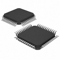
44-pin LQFP
Case:
10 x 10 mm2
64-pin LQFP
Case:
10 x 10 mm2
MC56F825x/MC56F824x
Digital Signal Controller
The MC56F825x/MC56F824x is a member of the 56800E
core-based family of digital signal controllers (DSCs). It
combines, on a single chip, the processing power of a DSP
and the functionality of a microcontroller with a flexible set of
peripherals to create a cost-effective solution. Because of its
low cost, configuration flexibility, and compact program
code, it is well-suited for many applications. The
MC56F825x/MC56F824x includes many peripherals that are
especially useful for cost-sensitive applications, including:
• Industrial control
• Home appliances
• Smart sensors
• Fire and security systems
• Solar inverters
• Battery chargers and management
• Switched-mode power supplies and power management
• Power metering
• Motor control (ACIM, BLDC, PMSM, SR, and stepper)
• Handheld power tools
• Arc detection
• Medical devices/equipment
• Instrumentation
• Lighting ballast
The 56800E core is based on a modified Harvard-style
architecture consisting of three execution units operating in
parallel, allowing as many as six operations per instruction
cycle. The MCU-style programming model and optimized
instruction set allow straightforward generation of efficient,
compact DSP and control code. The instruction set is also
highly efficient for C compilers to enable rapid development
of optimized control applications.
The MC56F825x/MC56F824x supports program execution
from internal memories. Two data operands per instruction
cycle can be accessed from the on-chip data RAM. A full set
of programmable peripherals supports various applications.
Each peripheral can be independently shut down to save
power. Any pin, except Power pins and the Reset pin, can also
be configured as General Purpose Input/Outputs (GPIOs).
48-pin LQFP
Case:
7 x 7 mm2
On-chip features include:
• 60 MHz operation frequency
• DSP and MCU functionality in a unified, C-efficient
architecture
• On-chip memory
– 56F8245/46: 48 KB (24K x 16) flash memory; 6 KB
(3K x 16) unified data/program RAM
– 56F8247: 48 KB (24K x 16) flash memory; 8 KB
(4K x 16) unified data/program RAM
– 56F8255/56/57: 64 KB (32K x 16) flash memory; 8 KB
(4K x 16) unified data/program RAM
• eFlexPWM with up to 9 channels, including 6 channels
with high (520 ps) resolution NanoEdge placement
• Two 8-channel, 12-bit analog-to-digital converters (ADCs)
with dynamic x2 and x4 programmable amplifier,
conversion time as short as 600 ns, and input
current-injection protection
• Three analog comparators with integrated 5-bit DAC
references
• Cyclic Redundancy Check (CRC) Generator
• Two high-speed queued serial communication interface
(QSCI) modules with LIN slave functionality
• Queued serial peripheral interface (QSPI) module
• Two SMBus-compatible inter-integrated circuit (I2C) ports
• Freescale’s scalable controller area network (MSCAN) 2.0
A/B module
• Two 16-bit quad timers (2 x 4 16-bit timers)
• Computer operating properly (COP) watchdog module
• On-chip relaxation oscillator: 8 MHz (400 kHz at standby
mode)
• Crystal/resonator oscillator
• Integrated power-on reset (POR) and low-voltage interrupt
(LVI) and brown-out reset module
• Inter-module crossbar connection
• Up to 54 GPIOs
• 44-pin LQFP, 48-pin LQFP, and 64-pin LQFP packages
• Single supply: 3.0 V to 3.6 V
Freescale reserves the right to change the detail specifications as may be required to permit
improvements in the design of its products.
© Freescale Semiconductor, Inc., 2009-2011, 2014. All rights reserved.
�Table of Contents
1
2
3
4
5
6
7
MC56F825x/MC56F824x Family Configuration . . . . . . . . . . . .3
Overview. . . . . . . . . . . . . . . . . . . . . . . . . . . . . . . . . . . . . . . . . .4
2.1 MC56F825x/MC56F824x Features. . . . . . . . . . . . . . . . .4
2.2 Award-Winning Development Environment . . . . . . . . . .8
2.3 Architecture Block Diagram . . . . . . . . . . . . . . . . . . . . . .8
2.4 Product Documentation . . . . . . . . . . . . . . . . . . . . . . . . 11
Signal/Connection Descriptions . . . . . . . . . . . . . . . . . . . . . . . 11
3.1 Introduction . . . . . . . . . . . . . . . . . . . . . . . . . . . . . . . . . . 11
3.2 Pin Assignment . . . . . . . . . . . . . . . . . . . . . . . . . . . . . . .15
3.3 MC56F825x/MC56F824x Signal Pins . . . . . . . . . . . . . .18
Memory Maps . . . . . . . . . . . . . . . . . . . . . . . . . . . . . . . . . . . . .29
4.1 Introduction . . . . . . . . . . . . . . . . . . . . . . . . . . . . . . . . . .29
4.2 Program Map . . . . . . . . . . . . . . . . . . . . . . . . . . . . . . . .30
4.3 Data Map . . . . . . . . . . . . . . . . . . . . . . . . . . . . . . . . . . .31
4.4 Interrupt Vector Table and Reset Vector . . . . . . . . . . . .33
4.5 Peripheral Memory-Mapped Registers . . . . . . . . . . . . .34
4.6 EOnCE Memory Map . . . . . . . . . . . . . . . . . . . . . . . . . .35
General System Control Information . . . . . . . . . . . . . . . . . . .36
5.1 Overview . . . . . . . . . . . . . . . . . . . . . . . . . . . . . . . . . . . .36
5.2 Power Pins . . . . . . . . . . . . . . . . . . . . . . . . . . . . . . . . . .36
5.3 Reset. . . . . . . . . . . . . . . . . . . . . . . . . . . . . . . . . . . . . . .36
5.4 On-chip Clock Synthesis. . . . . . . . . . . . . . . . . . . . . . . .37
5.5 Interrupt Controller . . . . . . . . . . . . . . . . . . . . . . . . . . . .39
5.6 System Integration Module (SIM) . . . . . . . . . . . . . . . . .39
5.7 Inter-Module Connections. . . . . . . . . . . . . . . . . . . . . . .40
5.8 Joint Test Action Group (JTAG)/Enhanced On-Chip
Emulator (EOnCE) . . . . . . . . . . . . . . . . . . . . . . . . . . . .46
Security Features . . . . . . . . . . . . . . . . . . . . . . . . . . . . . . . . . .46
6.1 Operation with Security Enabled. . . . . . . . . . . . . . . . . .46
6.2 Flash Access Lock and Unlock Mechanisms . . . . . . . .47
6.3 Product Analysis . . . . . . . . . . . . . . . . . . . . . . . . . . . . . .48
Specifications . . . . . . . . . . . . . . . . . . . . . . . . . . . . . . . . . . . . .48
7.1 General Characteristics . . . . . . . . . . . . . . . . . . . . . . . .48
7.2 Absolute Maximum Ratings . . . . . . . . . . . . . . . . . . . . .49
7.3 ESD Protection and Latch-up Immunity . . . . . . . . . . . .50
7.4 Thermal Characteristics . . . . . . . . . . . . . . . . . . . . . . . .50
7.5 Recommended Operating Conditions. . . . . . . . . . . . . .52
7.6 DC Electrical Characteristics . . . . . . . . . . . . . . . . . . . . 53
7.7 Supply Current Characteristics . . . . . . . . . . . . . . . . . . 55
7.8 Power-On Reset, Low Voltage Detection Specification 56
7.9 Voltage Regulator Specifications . . . . . . . . . . . . . . . . . 56
7.10 AC Electrical Characteristics . . . . . . . . . . . . . . . . . . . . 56
7.11 Enhanced Flex PWM Characteristics . . . . . . . . . . . . . 57
7.12 Flash Memory Characteristics . . . . . . . . . . . . . . . . . . . 57
7.13 External Clock Operation Timing . . . . . . . . . . . . . . . . . 57
7.14 Phase Locked Loop Timing . . . . . . . . . . . . . . . . . . . . . 58
7.15 External Crystal or Resonator Requirement . . . . . . . . 59
7.16 Relaxation Oscillator Timing . . . . . . . . . . . . . . . . . . . . 59
7.17 Reset, Stop, Wait, Mode Select, and Interrupt Timing. 60
7.18 Queued Serial Peripheral Interface (SPI) Timing . . . . 60
7.19 Queued Serial Communication Interface (SCI) Timing 64
7.20 Freescale’s Scalable Controller Area Network (MSCAN)65
7.21 Inter-Integrated Circuit Interface (I2C) Timing . . . . . . . 65
7.22 JTAG Timing . . . . . . . . . . . . . . . . . . . . . . . . . . . . . . . . 66
7.23 Quad Timer Timing . . . . . . . . . . . . . . . . . . . . . . . . . . . 67
7.24 COP Specifications . . . . . . . . . . . . . . . . . . . . . . . . . . . 68
7.25 Analog-to-Digital Converter (ADC) Parameters. . . . . . 68
7.26 Digital-to-Analog Converter (DAC) Parameters. . . . . . 70
7.27 5-Bit Digital-to-Analog Converter (DAC) Parameters . 71
7.28 HSCMP Specifications. . . . . . . . . . . . . . . . . . . . . . . . . 71
7.29 Optimize Power Consumption . . . . . . . . . . . . . . . . . . . 71
8 Design Considerations . . . . . . . . . . . . . . . . . . . . . . . . . . . . . 72
8.1 Thermal Design Considerations . . . . . . . . . . . . . . . . . 72
8.2 Electrical Design Considerations. . . . . . . . . . . . . . . . . 73
9 Ordering Information . . . . . . . . . . . . . . . . . . . . . . . . . . . . . . . 74
10 Package Mechanical Outline Drawings. . . . . . . . . . . . . . . . . 76
10.1 44-pin LQFP . . . . . . . . . . . . . . . . . . . . . . . . . . . . . . . . 76
10.2 48-pin LQFP . . . . . . . . . . . . . . . . . . . . . . . . . . . . . . . . 79
10.3 64-pin LQFP . . . . . . . . . . . . . . . . . . . . . . . . . . . . . . . . 81
11 Revision History . . . . . . . . . . . . . . . . . . . . . . . . . . . . . . . . . . 84
Appendix A
Interrupt Vector Table . . . . . . . . . . . . . . . . . . . . . . . . . . . . . . 85
MC56F825x/MC56F824x Digital Signal Controller, Rev. 4
2
Freescale Semiconductor
�MC56F825x/MC56F824x Family Configuration
1
MC56F825x/MC56F824x Family Configuration
Table 1 compares the MC56F825x/MC56F824x devices.
Table 1. MC56F825x/MC56F824x Device Comparison
Feature
56F8245 56F8246 56F8247 56F8255 56F8256 56F8257
Operation Frequency (MHz)
60
High Speed Peripheral Clock (MHz)
120
Flash memory size (KB) with 1024 words per page
48
48
48
64
64
64
RAM size (KB)
6
6
8
8
8
8
Enhanced
High resolution NanoEdge PWM (520 ps res.)
Flex PWM
Enhanced Flex PWM with Input Capture
(eFlexPWM)
PWM Fault Inputs (from Crossbar Input)
6
6
6
6
6
6
0
0
3
0
0
3
4
4
4
4
4
4
12-bit ADC with x1, 2x, 4x Programmable Gain
2 x 4Ch 2 x 5Ch 2 x 8Ch 2 x 4Ch 2 x 5 Ch 2 x 8 Ch
Analog comparators (ACMP) each with integrated 5-bit DAC
3
12-bit DAC
1
Cyclic Redundancy Check (CRC)
2C)
Inter-Integrated Circuit (I
Yes
/ SMBus
2
Queued Serial peripheral Interface (QSPI)
1
High speed Queued Serial Communications Interface (QSCI)1
2
Controller Area Network (MSCAN)
High Speed 16-bit multi-purpose timers (TMR)
0
1
2
8
Computer operating properly (COP) watchdog timer
Yes
Integrated Power-On Reset and low voltage detection
Yes
Phase-locked loop (PLL)
Yes
8 MHz (400 kHz at standby mode) on-chip ROSC
Yes
Crystal/resonator oscillator
Yes
Crossbar
Input pins
Output pins
General purpose I/O (GPIO)
3
6
6
6
6
6
6
2
2
6
2
2
6
35
39
54
35
39
54
IEEE 1149.1 Joint Test Action Group (JTAG) interface
Yes
Enhanced on-chip emulator (EOnCE)
Yes
Operating
temperature
range
V temperature devices
–40 °C to 105 °C
M temperature devices
–40 °C to 125 °C
Package
44LQFP 48LQFP 64LQFP 44LQFP 48LQFP 64LQFP
1
Can be clocked by high speed peripheral clock up to 120 MHz
Can be clocked by high speed peripheral clock up to 120 MHz
3
Shared with other function pins
2
MC56F825x/MC56F824x Digital Signal Controller, Rev. 4
Freescale Semiconductor
3
�Overview
2
Overview
2.1
MC56F825x/MC56F824x Features
2.1.1
•
•
•
•
•
•
•
•
•
•
•
•
•
•
2.1.2
•
•
•
2.1.3
•
•
•
•
•
•
Core
Efficient 56800E digital signal processor (DSP) engine with modified Harvard architecture
— Three internal address buses
— Four internal data buses
As many as 60 million instructions per second (MIPS) at 60 MHz core frequency
155 basic instructions in conjunction with up to 20 address modes
32-bit internal primary data buses supporting 8-bit, 16-bit, and 32-bit data movement, addition, subtraction, and logical
operation
Single-cycle 16 16-bit parallel multiplier-accumulator (MAC)
Four 36-bit accumulators, including extension bits
32-bit arithmetic and logic multi-bit shifter
Parallel instruction set with unique DSP addressing modes
Hardware DO and REP loops
Instruction set supports DSP and controller functions
Controller-style addressing modes and instructions for compact code
Efficient C compiler and local variable support
Software subroutine and interrupt stack with depth limited only by memory
JTAG/enhanced on-chip emulation (EOnCE) for unobtrusive, processor speed–independent, real-time debugging
Operation Range
3.0 V to 3.6 V operation (power supplies and I/O)
From power-on-reset: approximately 2.7 V to 3.6 V
Ambient temperature operating range
— V temperature devices: –40 °C to +105 °C
— M temperature devices: –40 °C to +125 °C
Memory
Dual Harvard architecture that permits as many as three simultaneous accesses to program and data memory
48 KB (24K x 16) to 64 KB (32K x 16) on-chip flash memory with 2048 bytes (1024 x 16) page size
6 KB (3K x 16) to 8 KB (4K x 16) on-chip RAM with byte addressable
EEPROM emulation capability using flash
Support for 60 MHz program execution from both internal flash and RAM memories
Flash security and protection that prevent unauthorized users from gaining access to the internal flash
MC56F825x/MC56F824x Digital Signal Controller, Rev. 4
4
Freescale Semiconductor
�Overview
2.1.4
•
•
•
•
•
Interrupt Controller
Five interrupt priority levels
— Three user programmable priority levels for each interrupt source: Level 0, 1, 2
— Unmaskable level 3 interrupts include: illegal instruction, hardware stack overflow, misaligned data access, and
SWI3 instruction
— Maskable level 3 interrupts include: EOnCE step counter, EOnCE breakpoint unit, and EOnCE trace buffer
— Lowest-priority software interrupt: level LP
Nested interrupts: higher priority level interrupt request can interrupt lower priority interrupt subroutine
Two programmable fast interrupts that can be assigned to any interrupt source
Notification to system integration module (SIM) to restart clock out of wait and stop states
Ability to relocate interrupt vector table
The masking of interrupt priority level is managed by the 56800E core.
2.1.5
•
Peripheral Highlights
One Enhanced Flex Pulse Width Modulator (eFlexPWM) module
— Up to nine output channels
— 16-bit resolution for center aligned, edge aligned, and asymmetrical PWMs
— Each complementary pair can operate with its own PWM frequency based and deadtime values
– 4 Time base
– Independent top and bottom deadtime insertion
— PWM outputs can operate as complimentary pairs or independent channels
— Independent control of both edges of each PWM output
— 6-channel NanoEdge high resolution PWM
– Fractional delay for enhanced resolution of the PWM period and edge placement
– Arbitrary eFlexPWM edge placement - PWM phase shifting
– NanoEdge implementation: 520 ps PWM frequency resolution
— 3 Channel PWM with full Input Capture features
– Three PWM Channels - PWMA, PWMB, and PWMX
– Enhanced input capture functionality
— Support for synchronization to external hardware or other PWM
— Double buffered PWM registers
– Integral reload rates from 1 to 16
– Half cycle reload capability
— Multiple output trigger events can be generated per PWM cycle via hardware
— Support for double switching PWM outputs
— Up to four fault inputs can be assigned to control multiple PWM outputs
– Programmable filters for fault inputs
— Independently programmable PWM output polarity
— Individual software control for each PWM output
— All outputs can be programmed to change simultaneously via a FORCE_OUT event
— PWMX pin can optionally output a third PWM signal from each submodule
— Channels not used for PWM generation can be used for buffered output compare functions
— Channels not used for PWM generation can be used for input capture functions
— Enhanced dual edge capture functionality
MC56F825x/MC56F824x Digital Signal Controller, Rev. 4
Freescale Semiconductor
5
�Overview
•
•
•
•
•
•
— Option to supply the source for each complementary PWM signal pair from any of the following:
– Crossbar module outputs
– External ADC input, taking into account values set in ADC high and low limit registers
Two independent 12-bit analog-to-digital converters (ADCs)
— 2 x 8 channel external inputs
— Built-in x1, x2, x4 programmable gain pre-amplifier
— Maximum ADC clock frequency: up to 10 MHz
– Single conversion time of 8.5 ADC clock cycles (8.5 x 100 ns = 850 ns)
– Additional conversion time of 6-ADC clock cycles (6 x 100 ns = 600 ns)
— Sequential, parallel, and independent scan mode
— First 8 samples have Offset, Limit and Zero-crossing calculation supported
— ADC conversions can be synchronized by eFlexPWM and timer modules via internal crossbar module
— Support for simultaneous and software triggering conversions
— Support for multi-triggering mode with a programmable number of conversions on each trigger
Inter-module Crossbar Switch (XBAR)
— Programmable internal module connections among the eFlexPWM, ADCs, Quad Timers, 12-bit DAC, HSCMPs,
and package pins
— User-defined input/output pins for PWM fault inputs, Timer input/output, ADC triggers, and Comparator outputs
Three analog comparators (CMPs)
— Selectable input source includes external pins, internal DACs
— Programmable output polarity
— Output can drive timer input, eFlexPWM fault input, eFlexPWM source, external pin output, and trigger ADCs
— Output falling and rising edge detection able to generate interrupts
— 32-tap programmable voltage reference per comparator
One 12-bit digital-to-analog converter (12-bit DAC)
— 12-bit resolution
— Power down mode
— Output can be routed to internal comparator, or off chip
Two four-channel 16-bit multi-purpose timer (TMR) modules
— Four independent 16-bit counter/timers with cascading capability per module
— Up to 120 MHz operating clock
— Each timer has capture and compare and quadrature decoder capability
— Up to 12 operating modes
— Four external inputs and two external outputs
Two queued serial communication interface (QSCI) modules with LIN slave functionality
— Up to 120 MHz operating clock
— Four-byte-deep FIFOs available on both transmit and receive buffers
— Full-duplex or single-wire operation
— Programmable 8- or 9-bit data format
— 13-bit integer and 3-bit fractional baud rate selection
— Two receiver wakeup methods:
– Idle line
– Address mark
— 1/16 bit-time noise detection
— Support LIN slave operation
MC56F825x/MC56F824x Digital Signal Controller, Rev. 4
6
Freescale Semiconductor
�Overview
•
•
•
•
•
•
•
•
One queued serial peripheral interface (QSPI) module
— Full-duplex operation
— Four-word deep FIFOs available on both transmit and receive buffers
— Master and slave modes
— Programmable length transactions (2 to 16 bits)
— Programmable transmit and receive shift order (MSB as first or last bit transmitted)
— Maximum slave module frequency = module clock frequency/2
— 13-bit baud rate divider for low speed communication
Two inter-integrated circuit (I2C) ports
— Operation at up to 100 kbps
— Support for master and slave operation
— Support for 10-bit address mode and broadcasting mode
— Support for SMBus, Version 2
One Freescale Scalable Controller Area Network (MSCAN) module
— Fully compliant with CAN protocol Version 2.0 A/B
— Support for standard and extended data frames
— Support for data rate up to 1 Mbit/s
— Five receive buffers and three transmit buffers
Computer operating properly (COP) watchdog timer capable of selecting different clock sources
— Programmable prescaler and timeout period
— Programmable wait, stop, and partial powerdown mode operation
— Causes loss of reference reset 128 cycles after loss of reference clock to the PLL is detected
— Choice of clock sources from four sources in support of EN60730 and IEC61508:
– On-chip relaxation oscillator
– External crystal oscillator/external clock source
– System clock (IP bus to 60 MHz)
Power supervisor (PS)
— On-chip linear regulator for digital and analog circuitry to lower cost and reduce noise
— Integrated low voltage detection to generate warning interrupt if VDD is below low voltage detection (LVI)
threshold
— Integrated power-on reset (POR)
– Reliable reset process during power-on procedure
– POR is released after VDD passes low voltage detection (LVI) threshold
— Integrated brown-out reset
— Run, wait, and stop modes
Phase lock loop (PLL) providing a high-speed clock to the core and peripherals
— 2x system clock provided to Quad Timers and SCIs
— Loss of lock interrupt
— Loss of reference clock interrupt
Clock sources
— On-chip relaxation oscillator with two user selectable frequencies: 400 kHz for low speed mode, 8 MHz for
normal operation
— External clock: crystal oscillator, ceramic resonator, and external clock source
Cyclic Redundancy Check (CRC) Generator
— Hardware CRC generator circuit using 16-bit shift register
MC56F825x/MC56F824x Digital Signal Controller, Rev. 4
Freescale Semiconductor
7
�Overview
—
—
—
—
—
•
•
2.1.6
•
•
•
•
2.2
CRC16-CCITT compliancy with x16 + x12 + x5 + 1 polynomial
Error detection for all single, double, odd, and most multi-bit errors
Programmable initial seed value
High-speed hardware CRC calculation
Optional feature to transpose input data and CRC result via transpose register, required on applications where
bytes are in LSb (Least Significant bit) format.
Up to 54 general-purpose I/O (GPIO) pins
— 5 V tolerant I/O
— Individual control for each pin to be in peripheral or GPIO mode
— Individual input/output direction control for each pin in GPIO mode
— Individual control for each output pin to be in push-pull mode or open-drain mode
— Hysteresis and configurable pullup device on all input pins
— Ability to generate interrupt with programmable rising or falling edge and software interrupt
— Configurable drive strength: 4 mA / 8 mA sink/source current
JTAG/EOnCE debug programming interface for real-time debugging
— IEEE 1149.1 Joint Test Action Group (JTAG) interface
— EOnCE interface for real-time debugging
Power Saving Features
Low-speed run, wait, and stop modes: as low as 781 Hz clock provided by OCCS and internal ROSC
Large regulator standby mode available for reducing power consumption at low-speed mode
Less than 30 µs typical wakeup time from stop modes
Each peripheral can be individually disabled to save power
Award-Winning Development Environment
Processor Expert (PE) provides a Rapid Application Design (RAD) tool that combines easy-to-use component-based software
application creation with an expert knowledge system.
The CodeWarrior Integrated Development Environment (IDE) is a sophisticated tool for code navigation, compiling, and
debugging. A complete set of evaluation modules (EVMs), demonstration board kit, and development system cards supports
concurrent engineering. Together, PE, CodeWarrior, and EVMs create a complete, scalable tools solution for easy, fast, and
efficient development.
2.3
Architecture Block Diagram
The MC56F825x/MC56F824x’s architecture appears in Figure 1 and Figure 2. Figure 1 illustrates how the 56800E system
buses communicate with internal memories and the IP bus interface as well as the internal connections among the units of the
56800E core.
MC56F825x/MC56F824x Digital Signal Controller, Rev. 4
8
Freescale Semiconductor
�Overview
DSP56800E Core
Program Control Unit
PC
LA
LA2
HWS0
HWS1
FIRA
OMR
SR
LC
LC2
FISR
Address
Generation
Unit
(AGU)
Instruction
Decoder
Interrupt
Unit
ALU1
ALU2
R0
R1
R2
R3
R4
R5
N
SP
M01
N3
Looping
Unit
Program
Memory
XAB1
XAB2
PAB
PDB
Data/
Program
RAM
CDBW
CDBR
XDB2
A2
B2
C2
D2
BitManipulation
Unit
Enhanced
OnCE™
JTAG TAP
Y
A1
B1
C1
D1
Y1
Y0
X0
MAC and ALU
A0
B0
C0
D0
IP Bus
Interface
Data
Arithmetic
Logic Unit
(ALU)
Multi-Bit Shifter
Figure 1. 56800E Core Block Diagram
Figure 2 shows the peripherals and control blocks connected to the IP bus bridge. Refer to the system integration module (SIM)
section in the device’s reference manual for information about which signals are multiplexed with those of other peripherals.
MC56F825x/MC56F824x Digital Signal Controller, Rev. 4
Freescale Semiconductor
9
�Overview
3RUW�$
*3,2$��
*3,2$��
*3,2$��
*3,2$��
*3,2$��
*3,2$��
*3,2$��
*3,2$�
3RUW�%
*3,2%��
*3,2%��
*3,2%��
*3,2%��
*3,2%��
*3,2%��
*3,2%��
*3,2%�
3RUW�&
*3,2&��
*3,2&��
*3,2&��
*3,2&��
*3,2&��
*3,2&��
*3,2&��
*3,2&��
*3,2&��
*3,2&��
*3,2&��
*3,2&��
*3,2&��
*3,2&��
*3,2&��
*3,2&�
3RUW�'
*3,2'��
*3,2'��
*3,2'��
*3,2'�
3RUW�(
*3,2(��
*3,2(��
*3,2(��
*3,2(��
*3,2(��
*3,2(��
*3,2(��
*3,2(�
3RUW�)
,3%XV�%ULGJH
*3,2)��
*3,2)��
*3,2)��
*3,2)��
*3,2)��
*3,2)��
*3,2)��
*3,2)�
)ODVK�,QWHUIDFH �� .%�)ODVK�$UUD\
,QWHUUXSW�&RQWUROOHU��,17&�
&\FOLF�5HGXQGDQF\�&KHFN��&5&�� 526&�
&ORFN
&RPSXWHU�2SHUDWLQJ�3URSHUO\��&23�
6\VWHP�
&ORFN
&26&�&ORFN�
2Q�&KLS�&ORFN�
6\QWKHVLV��2&&6�
&26&�
526&
6\VWHP�,QWHJUDWLRQ�0RGXOH��6,0�
&U\VWDO
5(6(7
3RZHU�0DQDJHPHQW�&RQWUROOHU
&RQWUROOHU�$UHD�1HWZRUN�
�06&$1�
4XHXHG�6HULDO�3HULSKHUDO�
,QWHUIDFH��463,��
4XHXHG�6HULDO�&RPPXQLFDWLRQV�
,QWHUIDFH����46&,��
4XHXHG�6HULDO�&RPPXQLFDWLRQV�
,QWHUIDFH����46&,��
,QWHU�,QWHJUDWHG�&LUFXLW���60%XV�
0RGXOH����,,&��
4XDG�7LPHU�0RGXOH�$��705$�
4XDG�7LPHU�0RGXOH�%��705%�
(QKDQFHG�)OH[�3:0��H)OH[3:0�
���ELW�'$&
*3,2�08;
,QWHU�,QWHJUDWHG�&LUFXLW���60%XV�
0RGXOH����,,&��
���ELW�$'&�$
���ELW�$'&�%
6


 工商网监
湘ICP备2023018690号
工商网监
湘ICP备2023018690号
