Freescale Semiconductor, Inc.
TECHNICAL DATA
Freescale Semiconductor, Inc...
MC68HC05X16
Freescale Semiconductor, Inc...
Freescale Semiconductor, Inc.
MC68HC05X16/D
Rev. 1
HC05
MC68HC05X16
MC68HC05X32
MC68HC705X32
TECHNICAL
DATA
For More Information On This Product,
Go to: www.freescale.com
�Freescale Semiconductor, Inc.
Freescale Semiconductor, Inc...
Freescale Semiconductor, Inc...
Freescale Semiconductor, Inc.
For More Information On This Product,
Go to: www.freescale.com
For More Information On This Product,
Go to: www.freescale.com
�Freescale Semiconductor, Inc.
Freescale Semiconductor, Inc...
Freescale Semiconductor, Inc...
Freescale Semiconductor, Inc.
INTRODUCTION
1
MODES OF OPERATION AND PIN DESCRIPTIONS
2
MEMORY AND REGISTERS
3
INPUT/OUTPUT PORTS
4
MOTOROLA CAN MODULE (MCAN)
5
PROGRAMMABLE TIMER
6
SERIAL COMMUNICATIONS INTERFACE
7
PULSE LENGTH D/A CONVERTERS
8
ANALOG TO DIGITAL CONVERTER
9
RESETS AND INTERRUPTS
10
CPU CORE AND INSTRUCTION SET
11
ELECTRICAL SPECIFICATIONS
12
MECHANICAL DATA
13
ORDERING INFORMATION
14
APPENDICES
15
For More Information On This Product,
Go to: www.freescale.com
For More Information On This Product,
Go to: www.freescale.com
1
�Freescale Semiconductor, Inc.
1
INTRODUCTION
2
MODES OF OPERATION AND PIN DESCRIPTIONS
3
MEMORY AND REGISTERS
4
INPUT/OUTPUT PORTS
5
MOTOROLA CAN MODULE (MCAN)
6
PROGRAMMABLE TIMER
7
SERIAL COMMUNICATIONS INTERFACE
8
PULSE LENGTH D/A CONVERTERS
9
ANALOG TO DIGITAL CONVERTER
Freescale Semiconductor, Inc...
Freescale Semiconductor, Inc...
Freescale Semiconductor, Inc.
10
RESETS AND INTERRUPTS
11
CPU CORE AND INSTRUCTION SET
12
ELECTRICAL SPECIFICATIONS
13
MECHANICAL DATA
14
ORDERING INFORMATION
15
APPENDICES
For More Information On This Product,
Go to: www.freescale.com
For More Information On This Product,
Go to: www.freescale.com
2
�Freescale Semiconductor, Inc.
MC68HC05X16
MC68HC05X32
MC68HC705X32
Freescale Semiconductor, Inc...
Freescale Semiconductor, Inc...
Freescale Semiconductor, Inc.
High-density complementary
metal oxide semiconductor
(HCMOS) microcontroller unit
RoHS-compliant and/or Pb- free versions of Freescale products have the functionality
and electrical characteristics of their non-RoHS-compliant and/or non-Pb- free
counterparts. For further information, see http://www.freescale.com or contact your
Freescale sales representative.
For information on Freescale.s Environmental Products program, go to
http://www.freescale.com/epp.
Information in this document is provided solely to enable system and software
implementers to use Freescale Semiconductor products. There are no express or
implied copyright licenses granted hereunder to design or fabricate any integrated
circuits or integrated circuits based on the information in this document.
Freescale Semiconductor reserves the right to make changes without further notice to
any products herein. Freescale Semiconductor makes no warranty, representation or
guarantee regarding the suitability of its products for any particular purpose, nor does
Freescale Semiconductor assume any liability arising out of the application or use of
any product or circuit, and specifically disclaims any and all liability, including without
limitation consequential or incidental damages. “Typical” parameters which may be
provided in Freescale Semiconductor data sheets and/or specifications can and do
vary in different applications and actual performance may vary over time. All operating
parameters, including “Typicals” must be validated for each customer application by
customer’s technical experts. Freescale Semiconductor does not convey any license
under its patent rights nor the rights of others. Freescale Semiconductor products are
not designed, intended, or authorized for use as components in systems intended for
surgical implant into the body, or other applications intended to support or sustain life,
or for any other application in which the failure of the Freescale Semiconductor product
could create a situation where personal injury or death may occur. Should Buyer
purchase or use Freescale Semiconductor products for any such unintended or
unauthorized application, Buyer shall indemnify and hold Freescale Semiconductor
and its officers, employees, subsidiaries, affiliates, and distributors harmless against all
claims, costs, damages, and expenses, and reasonable attorney fees arising out of,
directly or indirectly, any claim of personal injury or death associated with such
unintended or unauthorized use, even if such claim alleges that Freescale
Semiconductor was negligent regarding the design or manufacture of the part.
For More Information On This Product,
Go to: www.freescale.com
For More Information On This Product,
Go to: www.freescale.com
3
�Freescale Semiconductor, Inc.
Freescale Semiconductor, Inc...
Freescale Semiconductor, Inc...
Freescale Semiconductor, Inc.
Conventions
Where abbreviations are used in the text, an explanation can be found in the
glossary, at the back of this manual. Register and bit mnemonics are defined in the
paragraphs describing them.
An overbar is used to designate an active-low signal, eg: RESET.
Unless otherwise stated, a shaded cell in a register diagram indicates that the bit is
either unused or reserved; ‘u’ is used to indicate an undefined state (on reset).
Unless otherwise stated, a pin labelled as ‘NU’ should be tied to VSS in an electrically
noisy environment. Pins labelled ‘NC’ can be left floating, since they are not bonded
to any part of the device.
For More Information On This Product,
Go to: www.freescale.com
For More Information On This Product,
Go to: www.freescale.com
4
�Freescale Semiconductor, Inc.
CUSTOMER FEEDBACK QUESTIONNAIRE (MC68HC05X16/D)
Motorola wishes to continue to improve the quality of its documentation. We would welcome your feedback on the publication you
have just received. Having used the document, please complete this card (or a photocopy of it, if you prefer).
1.
How would you rate the quality of the document? Check one box in each category.
Excellent
Organization
Readability
Understandability
Accuracy
Illustrations
❏
❏
❏
❏
❏
Poor
❏
❏
❏
❏
❏
❏
❏
❏
❏
❏
❏
❏
❏
❏
❏
Excellent
❏
❏
❏
❏
❏
Tables
Table of contents
Index
Page size/binding
Overall impression
Poor
❏
❏
❏
❏
❏
❏
❏
❏
❏
❏
❏
❏
❏
❏
❏
Comments:
2.
What is your intended use for this document? If more than one option applies, please rank them (1, 2, 3).
❏
❏
❏
Selection of device for new application
System design
Training purposes
3.
– Cut along this line to remove –
Other
❏
Please specify:
How well does this manual enable you to perform the task(s) outlined in question 2?
Completely
Not at all
Comments:
❏ ❏ ❏ ❏
4.
How easy is it to find the information you are looking for?
Easy
Difficult
Comments:
❏ ❏ ❏ ❏
5.
Is the level of technical detail in the following sections sufficient to allow you to understand how the device functions?
Too little detail
SECTION 1
INTRODUCTION
SECTION 2
MODES OF OPERATION AND PIN DESCRIPTIONS
SECTION 3
MEMORY AND REGISTERS
SECTION 4
INPUT/OUTPUT PORTS
SECTION 5
MOTOROLA CAN MODULE (MCAN)
SECTION 6
PROGRAMMABLE TIMER
SECTION 7
SERIAL COMMUNICATIONS INTERFACE
SECTION 8
PULSE LENGTH D/A CONVERTERS
SECTION 9
ANALOG TO DIGITAL CONVERTER
SECTION 10
RESETS AND INTERRUPTS
SECTION 11
CPU CORE AND INSTRUCTION SET
SECTION 12
ELECTRICAL SPECIFICATIONS
SECTION 13
MECHANICAL DATA
SECTION 14
ORDERING INFORMATION
SECTION 15
APPENDICES
❏
❏
❏
❏
❏
❏
❏
❏
❏
❏
❏
❏
❏
❏
❏
❏
❏
❏
❏
❏
❏
❏
❏
❏
❏
❏
❏
❏
❏
❏
Too much detail
❏
❏
❏
❏
❏
❏
❏
❏
❏
❏
❏
❏
❏
❏
❏
❏
❏
❏
❏
❏
❏
❏
❏
❏
❏
❏
❏
❏
❏
❏
❏
❏
❏
❏
❏
❏
❏
❏
❏
❏
❏
❏
❏
❏
❏
Comments:
✂
Freescale Semiconductor, Inc...
Freescale Semiconductor, Inc...
Freescale Semiconductor, Inc.
6.
Have you found any errors? If so, please comment:
7.
From your point of view, is anything missing from the document? If so, please say what:
For More Information On This Product,
Go to: www.freescale.com
For More Information On This Product,
Go to: www.freescale.com
5
�8.
How could we improve this document?
9.
How would you rate Motorola’s documentation?
Excellent
– In general
– Against other semiconductor suppliers
✂
Freescale Semiconductor, Inc.
Poor
❏ ❏ ❏ ❏
❏ ❏ ❏ ❏
11. Which company (in any field) provides the best technical documentation?
12. How many years have you worked with microprocessors?
Less than 1 year
❏
1–3 years
❏
3–5 years
❏
More than 5 years
❏
– Second fold back along this line –
NE PAS AFFRANCHIR
By air mail
Par avion
IBRS NUMBER PHQ-B/207/G
CCRI NUMERO PHQ-B/207/G
NO STAMP REQUIRED
REPONSE PAYEE
GRANDE-BRETAGNE
Motorola Ltd.,
Colvilles Road,
Kelvin Industrial Estate,
EAST KILBRIDE,
G75 8BR.
GREAT BRITAIN.
Semiconductor Products Sector
– Cut along this line to remove –
Freescale Semiconductor, Inc...
10. Which semiconductor manufacturer provides the best technical documentation?
– First fold back along this line –
Freescale Semiconductor, Inc...
Freescale Semiconductor, Inc.
F.A.O. Technical Publications Manager
(re: MC68HC05X16/D)
– Third fold back along this line –
13. Currently there is some discussion in the semiconductor industry regarding a move towards providing data sheets in electronic
form. If you have any opinion on this subject, please comment.
14. We would be grateful if you would supply the following information (at your discretion), or attach your card.
Name:
Phone No:
Position:
FAX No:
Department:
Company:
Address:
or helping us improve our documentation,
echnical Publications Manager, Motorola Ltd., Scotland.
For More Information On This Product,
Go
to: tuck
www.freescale.com
– Finally,
this edge into opposite flap –
For More Information On This Product,
Go to: www.freescale.com
6
�Freescale Semiconductor, Inc.
TABLE OF CONTENTS
Freescale Semiconductor, Inc...
Freescale Semiconductor, Inc...
Freescale Semiconductor, Inc.
Paragraph
Number
TITLE
Page
Number
1
INTRODUCTION
1.1
1.2
Features ................................................................................................................ 1-2
Mask options for the MC68HC05X16 .................................................................... 1-3
2
MODES OF OPERATION AND
PIN DESCRIPTIONS
2.1
Modes of operation................................................................................................ 2-1
2.1.1
Single-chip mode ............................................................................................. 2-1
2.1.2
Bootstrap mode ............................................................................................... 2-2
2.1.2.1
Serial RAM loader ...................................................................................... 2-3
2.1.2.2
Jump to RAM + 1 ....................................................................................... 2-3
2.1.2.3
‘Jump to any address’ ................................................................................ 2-3
2.2
Low power modes ................................................................................................. 2-6
2.2.1
STOP mode ..................................................................................................... 2-6
2.2.2
WAIT mode ...................................................................................................... 2-7
2.2.2.1
Power consumption during WAIT mode ..................................................... 2-8
2.2.3
SLOW mode .................................................................................................... 2-8
2.2.3.1
Miscellaneous register .............................................................................. 2-10
2.3
Pin descriptions ..................................................................................................... 2-11
2.3.1
VDD and VSS .................................................................................................. 2-11
2.3.2
IRQ .................................................................................................................. 2-11
2.3.3
RESET............................................................................................................. 2-11
2.3.4
MDS................................................................................................................. 2-12
2.3.5
TCAP1 ............................................................................................................. 2-12
2.3.6
TCAP2 ............................................................................................................. 2-12
2.3.7
TCMP1............................................................................................................. 2-12
2.3.8
TCMP2............................................................................................................. 2-12
2.3.9
RDI (Receive data in)....................................................................................... 2-12
2.3.10
TDO (Transmit data out) .................................................................................. 2-12
2.3.11
SCLK ............................................................................................................... 2-13
MC68HC05X16
TABLE OF CONTENTS
For More Information On This Product,
Go to: www.freescale.com
For More Information On This Product,
Go to: www.freescale.com
i
7
�Freescale Semiconductor, Inc.
Paragraph
Number
Freescale Semiconductor, Inc...
Freescale Semiconductor, Inc...
Freescale Semiconductor, Inc.
2.3.12
2.3.12.1
2.3.12.2
2.3.12.3
2.3.12.4
2.3.13
2.3.14
2.3.15
2.3.16
2.3.17
2.3.18
2.3.19
2.3.20
2.3.21
2.3.22
2.3.23
2.3.24
2.3.25
TITLE
Page
Number
OSC1, OSC2 ................................................................................................... 2-13
Crystal........................................................................................................ 2-13
Ceramic resonator ..................................................................................... 2-13
External clock............................................................................................. 2-13
Oscillator division ....................................................................................... 2-15
PLMA ............................................................................................................... 2-15
PLMB ............................................................................................................... 2-15
VPP1 ............................................................................................................... 2-16
VRH ................................................................................................................. 2-16
VRL.................................................................................................................. 2-16
PA0 – PA7/PB0 – PB7/PC0 – PC7 .................................................................. 2-16
NWOI ............................................................................................................... 2-16
PD0/AN0–PD7/AN7......................................................................................... 2-16
VDD1 ............................................................................................................... 2-17
VSS1 ............................................................................................................... 2-17
VDDH .............................................................................................................. 2-17
RX0/RX1.......................................................................................................... 2-17
TX0/TX1 .......................................................................................................... 2-17
3
MEMORY AND REGISTERS
3.1
3.2
3.3
3.4
3.5
3.5.1
3.5.2
3.5.3
3.5.4
3.5.5
3.6
3.7
3.8
Registers ............................................................................................................... 3-1
RAM ...................................................................................................................... 3-1
ROM ...................................................................................................................... 3-1
Bootstrap ROM...................................................................................................... 3-3
EEPROM............................................................................................................... 3-4
EEPROM control register ................................................................................ 3-4
EEPROM read operation ................................................................................. 3-6
EEPROM erase operation ............................................................................... 3-6
EEPROM programming operation ................................................................... 3-7
Options register (OPTR) .................................................................................. 3-7
EEPROM during STOP mode ............................................................................... 3-8
EEPROM during WAIT mode ................................................................................ 3-8
Miscellaneous register.......................................................................................... 3-11
4
INPUT/OUTPUT PORTS
4.1
4.2
4.3
4.4
4.5
Input/output programming ..................................................................................... 4-1
Ports A and B ........................................................................................................ 4-2
Port C .................................................................................................................... 4-3
Port D .................................................................................................................... 4-4
Port registers ......................................................................................................... 4-4
TABLE OF CONTENTS
For More Information On This Product,
Go to: www.freescale.com
For More Information On This Product,
Go to: www.freescale.com
MC68HC05X16
Rev. 1
8
�Freescale Semiconductor, Inc.
Paragraph
Number
TITLE
Page
Number
4.5.1
Port data registers A and B (PORTA and PORTB) .......................................... 4-4
4.5.2
Port data register C (PORTC).......................................................................... 4-5
4.5.3
Port data register D (PORTD).......................................................................... 4-5
4.5.4
A/D status/control register ............................................................................... 4-5
4.5.5
Data direction registers (DDRA, DDRB and DDRC)........................................ 4-6
4.6
Other port considerations ...................................................................................... 4-6
Freescale Semiconductor, Inc...
Freescale Semiconductor, Inc...
Freescale Semiconductor, Inc.
5
MOTOROLA CAN MODULE (MCAN)
5.1
5.2
5.3
5.3.1
5.3.2
5.3.3
5.3.4
5.3.5
5.3.6
5.3.7
5.3.8
5.3.9
5.3.10
5.3.11
5.3.12
5.3.13
5.3.14
5.3.15
5.4
5.4.1
5.5
5.5.1
TBF – Transmit buffer ............................................................................................ 5-4
RBF – Receive buffer ............................................................................................ 5-4
Interface to the MC68HC05X16 CPU.................................................................... 5-4
MCAN control register (CCNTRL) ................................................................... 5-6
MCAN command register (CCOM) .................................................................. 5-7
MCAN status register (CSTAT) ........................................................................ 5-10
MCAN interrupt register (CINT) ....................................................................... 5-12
MCAN acceptance code register (CACC)........................................................ 5-13
MCAN acceptance mask register (CACM) ...................................................... 5-14
MCAN bus timing register 0 (CBT0) ................................................................ 5-14
MCAN bus timing register 1 (CBT1) ................................................................ 5-16
MCAN output control register (COCNTRL)...................................................... 5-18
Transmit buffer identifier register (TBI)............................................................. 5-20
Remote transmission request and data length code register (TRTDL)............ 5-20
Transmit data segment registers (TDS) 1 – 8 .................................................. 5-21
Receive buffer identifier register (RBI) ............................................................. 5-21
Remote transmission request and data length code register (RRTDL) ........... 5-22
Receive data segment registers (RDS) 1 – 8 .................................................. 5-22
Interface to the MCAN bus .................................................................................... 5-22
Single wire operation ....................................................................................... 5-24
Sleep mode ........................................................................................................... 5-24
Sleep comparator reference ............................................................................ 5-25
6
PROGRAMMABLE TIMER
6.1
Counter.................................................................................................................. 6-1
6.1.1
Counter register and alternate counter register ............................................... 6-3
6.2
Timer control and status ........................................................................................ 6-4
6.2.1
Timer control register (TCR) ............................................................................ 6-4
6.2.2
Timer status register (TSR) ............................................................................. 6-6
6.3
Input capture.......................................................................................................... 6-7
6.3.1
Input capture register 1 (ICR1) ........................................................................ 6-7
6.3.2
Input capture register 2 (ICR2) ........................................................................ 6-8
MC68HC05X16
TABLE OF CONTENTS
For More Information On This Product,
Go to: www.freescale.com
For More Information On This Product,
Go to: www.freescale.com
iii
9
�Freescale Semiconductor, Inc.
Paragraph
Number
Freescale Semiconductor, Inc...
Freescale Semiconductor, Inc...
Freescale Semiconductor, Inc.
6.4
6.4.1
6.4.2
6.4.3
6.5
6.5.1
6.6
6.7
6.8
TITLE
Page
Number
Output compare..................................................................................................... 6-9
Output compare register 1 (OCR1) ................................................................. 6-9
Output compare register 2 (OCR2) ................................................................. 6-10
Software force compare................................................................................... 6-11
Pulse length modulation (PLM) ............................................................................. 6-11
Pulse length modulation registers A and B (PLMA/PLMB).............................. 6-11
Timer during STOP mode ..................................................................................... 6-12
Timer during WAIT mode ...................................................................................... 6-12
Timer state diagrams............................................................................................. 6-12
7
SERIAL COMMUNICATIONS INTERFACE
7.1
7.2
7.3
7.4
7.5
7.6
7.6.1
7.6.2
7.7
7.8
7.9
7.10
7.11
7.11.1
7.11.2
7.11.3
7.11.4
7.11.5
7.12
7.13
7.14
SCI two-wire system features................................................................................ 7-1
SCI receiver features............................................................................................. 7-3
SCI transmitter features......................................................................................... 7-3
Functional description ........................................................................................... 7-3
Data format............................................................................................................ 7-5
Receiver wake-up operation.................................................................................. 7-5
Idle line wake-up.............................................................................................. 7-6
Address mark wake-up .................................................................................... 7-6
Receive data in (RDI) ............................................................................................ 7-6
Start bit detection .................................................................................................. 7-6
Transmit data out (TDO)........................................................................................ 7-8
SCI synchronous transmission.............................................................................. 7-9
SCI registers.......................................................................................................... 7-10
Serial communications data register (SCDR) .................................................. 7-10
Serial communications control register 1 (SCCR1) ......................................... 7-10
Serial communications control register 2 (SCCR2) ......................................... 7-14
Serial communications status register (SCSR) ............................................... 7-16
Baud rate register (BAUD) ............................................................................... 7-18
Baud rate selection................................................................................................ 7-20
SCI during STOP mode......................................................................................... 7-21
SCI during WAIT mode.......................................................................................... 7-21
8
PULSE LENGTH D/A CONVERTERS
8.1
8.2
8.3
8.4
Miscellaneous register........................................................................................... 8-3
PLM clock selection............................................................................................... 8-4
PLM during STOP mode ....................................................................................... 8-4
PLM during WAIT mode ........................................................................................ 8-4
TABLE OF CONTENTS
For More Information On This Product,
Go to: www.freescale.com
For More Information On This Product,
Go to: www.freescale.com
MC68HC05X16
Rev. 1
10
�Freescale Semiconductor, Inc.
Paragraph
Number
TITLE
Page
Number
9
ANALOG TO DIGITAL CONVERTER
Freescale Semiconductor, Inc...
Freescale Semiconductor, Inc...
Freescale Semiconductor, Inc.
9.1
9.2
9.2.1
9.2.2
9.2.3
9.3
9.4
9.5
A/D converter operation......................................................................................... 9-1
A/D registers.......................................................................................................... 9-3
Port D data register (PORTD).......................................................................... 9-3
A/D result data register (ADDATA) ................................................................... 9-3
A/D status/control register (ADSTAT)............................................................... 9-4
A/D converter during STOP mode......................................................................... 9-5
A/D converter during WAIT mode.......................................................................... 9-6
Port D analog input................................................................................................ 9-6
10
RESETS AND INTERRUPTS
10.1 Resets ................................................................................................................. 10-1
10.1.1
Power-on reset............................................................................................... 10-2
10.1.2
Miscellaneous register .................................................................................. 10-2
10.1.3
RESET pin ..................................................................................................... 10-3
10.1.4
Computer operating properly (COP) watchdog reset .................................... 10-3
10.1.4.1
COP watchdog during STOP mode ......................................................... 10-5
10.1.4.2
COP watchdog during WAIT mode .......................................................... 10-5
10.1.5
Functions affected by reset............................................................................ 10-5
10.2 Interrupts ............................................................................................................. 10-7
10.2.1
Interrupt priorities........................................................................................... 10-9
10.2.2
Nonmaskable software interrupt (SWI) .......................................................... 10-9
10.2.3
Maskable hardware interrupts........................................................................ 10-9
10.2.3.1
Miscellaneous register ............................................................................. 10-10
10.2.3.2
External interrupts.................................................................................... 10-11
10.2.3.3
MCAN interrupt (CIRQ) ............................................................................ 10-11
10.2.3.4
Timer interrupts ........................................................................................ 10-12
10.2.3.5
Serial communications interface (SCI) interrupts..................................... 10-12
10.2.4
Hardware controlled interrupt sequence........................................................ 10-13
11
CPU CORE AND INSTRUCTION SET
11.1 Registers ............................................................................................................. 11-1
11.1.1
Accumulator (A) ............................................................................................. 11-1
11.1.2
Index register (X) ........................................................................................... 11-2
11.1.3
Program counter (PC).................................................................................... 11-2
11.1.4
Stack pointer (SP).......................................................................................... 11-2
11.1.5
Condition code register (CCR)....................................................................... 11-2
11.2 Instruction set ...................................................................................................... 11-3
MC68HC05X16
TABLE OF CONTENTS
For More Information On This Product,
Go to: www.freescale.com
For More Information On This Product,
Go to: www.freescale.com
v
11
�Freescale Semiconductor, Inc.
Paragraph
Number
Freescale Semiconductor, Inc...
Freescale Semiconductor, Inc...
Freescale Semiconductor, Inc.
TITLE
Page
Number
11.2.1
Register/memory Instructions........................................................................ 11-4
11.2.2
Branch instructions ........................................................................................ 11-4
11.2.3
Bit manipulation instructions.......................................................................... 11-4
11.2.4
Read/modify/write instructions....................................................................... 11-4
11.2.5
Control instructions........................................................................................ 11-4
11.2.6
Tables ............................................................................................................ 11-4
11.3 Addressing modes............................................................................................... 11-11
11.3.1
Inherent ......................................................................................................... 11-11
11.3.2
Immediate ...................................................................................................... 11-11
11.3.3
Direct ............................................................................................................. 11-11
11.3.4
Extended ....................................................................................................... 11-12
11.3.5
Indexed, no offset .......................................................................................... 11-12
11.3.6
Indexed, 8-bit offset ....................................................................................... 11-12
11.3.7
Indexed, 16-bit offset ..................................................................................... 11-12
11.3.8
Relative.......................................................................................................... 11-13
11.3.9
Bit set/clear .................................................................................................... 11-13
11.3.10 Bit test and branch......................................................................................... 11-13
12
ELECTRICAL SPECIFICATIONS
12.1
12.2
12.3
12.4
12.5
12.6
Absolute maximum ratings .................................................................................. 12-1
DC electrical characteristics ............................................................................... 12-2
A/D converter characteristics .............................................................................. 12-4
Control timing ...................................................................................................... 12-5
MCAN bus interface DC electrical characteristics ............................................... 12-6
MCAN bus interface control timing characteristics .............................................. 12-6
13
MECHANICAL DATA
13.1
13.2
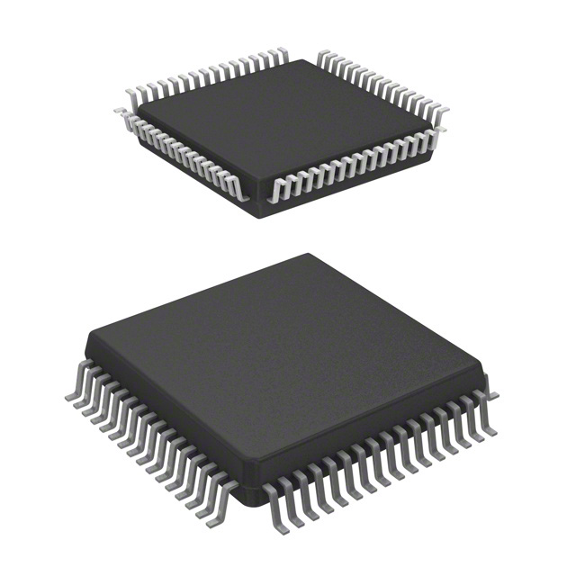
64-pin quad flat pack (QFP) pinout ..................................................................... 13-1
64-pin quad flat pack (QFP) mechanical dimensions.......................................... 13-2
14
ORDERING INFORMATION
14.1
14.2
14.3
EPROMS............................................................................................................. 14-2
Verification media ................................................................................................ 14-2
ROM verification units (RVU) .............................................................................. 14-2
TABLE OF CONTENTS
For More Information On This Product,
Go to: www.freescale.com
For More Information On This Product,
Go to: www.freescale.com
MC68HC05X16
Rev. 1
12
�Freescale Semiconductor, Inc.
Paragraph
Number
TITLE
Page
Number
A
MC68HC05X32
Freescale Semiconductor, Inc...
Freescale Semiconductor, Inc...
Freescale Semiconductor, Inc.
A.1
A.2
A.3
A.3.1
A.3.2
A.3.3
A.3.4
A.3.5
A.3.6
Features ................................................................................................................A-1
Memory map, register outline and block diagram..................................................A-2
Electrical specifications .........................................................................................A-6
Maximum ratings..............................................................................................A-6
DC electrical characteristics ...........................................................................A-7
A/D converter characteristics...........................................................................A-9
Control timing...................................................................................................A-10
MCAN bus interface DC electrical characteristics .................................................A-11
MCAN bus interface control timing characteristics ................................................A-12
B
MC68HC705X32
B.1
Features ................................................................................................................B-2
B.2
VPP6 .....................................................................................................................B-2
B.3
CANE.....................................................................................................................B-2
B.4
Block diagram, memory map and register outline .................................................B-3
B.5
EPROM .................................................................................................................B-7
B.5.1
EPROM read operation....................................................................................B-7
B.5.2
EPROM program operation .............................................................................B-8
B.5.3
EPROM/EEPROM/ECLK control register ........................................................B-8
B.6
EEPROM options register (OPTR) ........................................................................B-11
B.7
Mask option register (MOR) ..................................................................................B-12
B.8
Bootstrap mode .....................................................................................................B-14
B.8.1
Erased EPROM verification and EEPROM erasure ........................................B-17
B.8.2
EPROM/EEPROM parallel bootstrap...............................................................B-17
B.8.3
Serial RAM loader............................................................................................B-20
B.8.3.1
Jump to start of RAM ($0051) ....................................................................B-20
B.9
Electrical specifications .........................................................................................B-23
B.9.1
Maximum ratings..............................................................................................B-23
B.9.2
DC electrical characteristics ............................................................................B-24
B.9.3
EPROM electrical characteristics ....................................................................B-26
B.9.4
Control timing...................................................................................................B-27
B.9.5
A/D converter characteristics...........................................................................B-28
B.9.6
MCAN bus interface DC electrical characteristics ...........................................B-29
B.9.7
MCAN bus interface control timing characteristics ..........................................B-29
MC68HC05X16
TABLE OF CONTENTS
For More Information On This Product,
Go to: www.freescale.com
For More Information On This Product,
Go to: www.freescale.com
vii
13
�Freescale Semiconductor, Inc.
Paragraph
Number
TITLE
Page
Number
C
MC68HC05X32
HIGH SPEED OPERATION
C.1
C.2
DC electrical characteristics ..................................................................................C-1
Control Timing .......................................................................................................C-2
Freescale Semiconductor, Inc...
Freescale Semiconductor, Inc...
Freescale Semiconductor, Inc.
TABLE OF CONTENTS
For More Information On This Product,
Go to: www.freescale.com
For More Information On This Product,
Go to: www.freescale.com
MC68HC05X16
Rev. 1
14
�Freescale Semiconductor, Inc.
LIST OF FIGURES
Freescale Semiconductor, Inc...
Freescale Semiconductor, Inc...
Freescale Semiconductor, Inc.
Figure
Number
1-1
2-1
2-2
2-3
2-4
2-5
2-6
2-7
3-1
3-2
4-1
4-2
4-3
5-1
5-2
5-3
5-4
5-5
5-6
6-1
6-2
6-3
6-4
6-5
7-1
7-2
7-3
7-4
7-5
7-6
7-7
7-8
7-9
TITLE
Page
Number
MC68HC05X16 block diagram ............................................................................... 1-4
Bootstrap mode function selection flow chart......................................................... 2-2
MC68HC05X16 ‘jump to any address’ schematic diagram..................................... 2-4
MC68HC05X16 ‘load program in RAM and execute’ schematic diagram............... 2-5
STOP and WAIT flow charts................................................................................... 2-9
Slow mode divider block diagram ........................................................................... 2-10
Oscillator connections ............................................................................................ 2-14
Oscillator divider block diagram.............................................................................. 2-15
Memory map of the MC68HC05X16 ...................................................................... 3-2
MCAN module memory map .................................................................................. 3-3
Standard I/O port structure..................................................................................... 4-2
ECLK timing diagram ............................................................................................. 4-3
Port logic levels ...................................................................................................... 4-7
MCAN block diagram.............................................................................................. 5-1
MCAN frame formats.............................................................................................. 5-2
MCAN module memory map .................................................................................. 5-5
Oscillator block diagram ......................................................................................... 5-15
Segments within the bit time .................................................................................. 5-16
A typical physical interface between the MCAN and the MCAN bus lines ............. 5-23
16-bit programmable timer block diagram .............................................................. 6-2
Timer state timing diagram for reset....................................................................... 6-13
Timer state timing diagram for input capture .......................................................... 6-13
Timer state timing diagram for output compare...................................................... 6-14
Timer state timing diagram for timer overflow......................................................... 6-14
Serial communications interface block diagram ..................................................... 7-2
SCI rate generator division ..................................................................................... 7-4
Data format............................................................................................................. 7-5
SCI examples of start bit sampling technique ........................................................ 7-7
SCI sampling technique used on all bits ................................................................ 7-7
Artificial start following a framing error ................................................................... 7-8
SCI start bit following a break................................................................................. 7-8
SCI example of synchronous and asynchronous transmission .............................. 7-9
SCI data clock timing diagram (M=0) ..................................................................... 7-12
MC68HC05X16
LIST OF FIGURES
For More Information On This Product,
Go to: www.freescale.com
For More Information On This Product,
Go to: www.freescale.com
ix
15
�Freescale Semiconductor, Inc.
Figure
Number
Freescale Semiconductor, Inc...
Freescale Semiconductor, Inc...
Freescale Semiconductor, Inc.
7-10
8-1
8-2
8-3
9-1
9-2
10-1
10-2
10-3
10-4
11-1
11-2
12-1
13-1
13-2
A-1
A-2
A-3
B-1
B-2
B-3
B-4
B-5
B-6
B-7
B-8
B-9
TITLE
Page
Number
SCI data clock timing diagram (M=1) ......................................................................7-13
PLM system block diagram .....................................................................................8-1
PLM output waveform examples .............................................................................8-2
PLM clock selection ................................................................................................8-4
A/D converter block diagram ...................................................................................9-2
Electrical model of an A/D input pin ........................................................................9-6
Reset timing diagram ............................................................................................10-1
RESET external RC pull-down ..............................................................................10-3
Watchdog system block diagram...........................................................................10-4
Interrupt flow chart ................................................................................................10-8
Programming model ..............................................................................................11-1
Stacking order .......................................................................................................11-2
Timer relationship..................................................................................................12-5
64-pin QFP pinout .................................................................................................13-1
64-pin QFP mechanical dimensions .....................................................................13-2
MC68HC05X32 block diagram............................................................................... A-2
Memory map of the MC68HC05X32 ...................................................................... A-3
Timer relationship................................................................................................... A-11
MC68HC705X32 block diagram............................................................................. B-3
Memory map of the MC68HC705X32 .................................................................... B-5
Modes of operation flow chart ................................................................................ B-15
Timing diagram with handshake............................................................................. B-18
Parallel EPROM loader timing diagram.................................................................. B-18
EPROM parallel bootstrap schematic diagram ...................................................... B-19
RAM load and execute schematic diagram ............................................................ B-21
Parallel RAM loader timing diagram ....................................................................... B-22
Timer relationship................................................................................................... B-27
LIST OF FIGURES
For More Information On This Product,
Go to: www.freescale.com
For More Information On This Product,
Go to: www.freescale.com
MC68HC05X16
Rev. 1
16
�Freescale Semiconductor, Inc.
LIST OF TABLES
Freescale Semiconductor, Inc...
Freescale Semiconductor, Inc...
Freescale Semiconductor, Inc.
Table
Number
1-1
2-1
3-1
3-2
3-3
3-4
4-1
5-1
5-2
5-3
5-4
5-5
5-6
7-1
7-2
7-3
7-4
7-5
7-6
7-7
7-8
7-9
9-1
9-2
10-1
10-2
10-3
11-1
11-2
11-3
11-4
11-5
11-6
TITLE
Page
Number
Data sheet appendices........................................................................................... 1-1
Mode of operation selection ................................................................................... 2-1
EEPROM control bits description ........................................................................... 3-6
MC68HC05X16 register outline.............................................................................. 3-9
MCAN register outline ............................................................................................ 3-10
IRQ and WOI sensitivity ......................................................................................... 3-11
I/O pin states .......................................................................................................... 4-2
Synchronization jump width.................................................................................... 5-15
Baud rate prescaler ................................................................................................ 5-15
Time segment values ............................................................................................. 5-17
Output control modes ............................................................................................. 5-18
MCAN driver output levels...................................................................................... 5-19
Data length codes .................................................................................................. 5-21
Method of receiver wake-up ................................................................................... 7-11
SCI clock on SCLK pin ........................................................................................... 7-13
First prescaler stage............................................................................................... 7-18
Second prescaler stage (transmitter) ..................................................................... 7-18
Second prescaler stage (receiver) ......................................................................... 7-19
SCI baud rate selection with CPU clock frequency = fOSC/2.................................. 7-20
SCI baud rate selection with CPU clock frequency = fOSC/8.................................. 7-20
SCI baud rate selection with CPU clock frequency = fOSC/10................................ 7-20
SCI transmit baud rate output for a given prescaler output .................................... 7-21
A/D clock selection ................................................................................................. 9-4
A/D channel assignment ........................................................................................ 9-5
Effect of RESET, POR, STOP and WAIT.............................................................. 10-6
Interrupt priorities ................................................................................................. 10-9
IRQ and WOI sensitivity ....................................................................................... 10-10
MUL instruction .................................................................................................... 11-5
Register/memory instructions............................................................................... 11-5
Branch instructions............................................................................................... 11-6
Bit manipulation instructions................................................................................. 11-6
Read/modify/write instructions ............................................................................. 11-7
Control instructions............................................................................................... 11-7
MC68HC05X16
LIST OF TABLES
For More Information On This Product,
Go to: www.freescale.com
For More Information On This Product,
Go to: www.freescale.com
xi
17
�Freescale Semiconductor, Inc.
Table
Number
Freescale Semiconductor, Inc...
Freescale Semiconductor, Inc...
Freescale Semiconductor, Inc.
11-7
11-8
12-1
12-2
12-3
12-4
12-5
12-6
14-1
14-2
A-1
A-2
A-3
A-4
A-5
1-6
1-7
B-1
B-2
B-3
B-4
B-5
B-6
B-7
B-8
B-9
B-10
B-11
B-12
B-13
C-1
C-2
TITLE
Page
Number
Instruction set........................................................................................................11-8
M68HC05 opcode map .........................................................................................11-10
Absolute maximum ratings ....................................................................................12-1
DC electrical characteristics..................................................................................12-2
A/D characteristics ................................................................................................12-4
Control timing ........................................................................................................12-5
MCAN bus interface DC electrical characteristics.................................................12-6
MCAN bus interface control timing characteristics................................................12-6
MC order numbers ................................................................................................14-1
EPROMs for pattern generation ............................................................................14-2
Register outline ...................................................................................................... A-5
Maximum ratings .................................................................................................... A-6
DC electrical characteristics................................................................................... A-7
A/D characteristics ................................................................................................. A-9
Control timing ......................................................................................................... A-10
MCAN bus interface DC electrical characteristics.................................................. A-11
MCAN bus interface control timing characteristics................................................. A-12
Register outline ...................................................................................................... B-4
EPROM control bits description ............................................................................. B-9
EEPROM1 control bits description......................................................................... B-10
Clock divide ratio selection..................................................................................... B-12
Mode of operation selection ................................................................................... B-14
Bootstrap vector targets in RAM ............................................................................ B-20
Maximum ratings .................................................................................................... B-23
DC electrical characteristics................................................................................... B-24
EPROM electrical characteristics........................................................................... B-26
Control timing ......................................................................................................... B-27
A/D characteristics ................................................................................................. B-28
MCAN bus interface DC electrical characteristics.................................................. B-29
MCAN bus interface control timing characteristics................................................. B-29
DC electrical characteristics................................................................................... C-1
Control timing ......................................................................................................... C-2
LIST OF TABLES
For More Information On This Product,
Go to: www.freescale.com
For More Information On This Product,
Go to: www.freescale.com
MC68HC05X16
Rev. 1
18
�Freescale Semiconductor, Inc.
1
1
Freescale Semiconductor, Inc...
Freescale Semiconductor, Inc...
Freescale Semiconductor, Inc.
INTRODUCTION
The MC68HC05X16 microcomputer (MCU) is a member of Motorola’s MC68HC05 family of
low-cost single chip microcomputers. This 8-bit MCU contains an on-board controller area network
module (MCAN), complete with interface circuitry, comprising output drivers, input comparators
and a VDD/2 generator. In addition, the device contains an on-chip oscillator, CPU, RAM, ROM,
EEPROM, A/D converter, pulse length modulated outputs, I/O, serial communications interface,
programmable timer system and watchdog. The fully static design allows operation at frequencies
down to dc, reducing power consumption to a few micro-amps.
This data sheet is structured such that devices similar to the MC68HC05X16 are described in a
set of appendices (see Table 1-1).
Table 1-1 Data sheet appendices
Device
MC68HC05X32
MC68HC705X32
MC68HC05X32
Note:
Appendix
Differences from MC68HC05X16
A
32K bytes ROM; increased RAM
32K bytes EPROM; increased RAM; bootstrap firmware
B
replaced
C
32K bytes ROM; increased RAM; high speed operation
Appendix C contains only electrical characteristics exclusive to the high speed
operation of the MC68HC05X32. For all other information concerning this device, refer
to Appendix A.
MC68HC05X16
INTRODUCTION
For More Information On This Product,
Go to: www.freescale.com
For More Information On This Product,
Go to: www.freescale.com
1-1
19
�Freescale Semiconductor, Inc.
1
1.1
Features
Hardware features
Freescale Semiconductor, Inc...
Freescale Semiconductor, Inc...
Freescale Semiconductor, Inc.
•
Fully static design featuring the industry standard M68HC05 family CPU core
•
On chip crystal oscillator with divide-by -2, -4, -8 or -10, or a software selectable divide-by -32,
-64, -128 or -160 option (SLOW mode)
•
352 bytes of RAM
•
15102 bytes of user ROM plus 16 bytes of user vectors
•
256 bytes of byte erasable EEPROM with internal charge pump and security bit
•
Write/erase protect bit for 224 of the 256 bytes EEPROM
•
Bootstrap firmware
•
Power saving STOP, WAIT and SLOW modes
•
Three 8-bit parallel I/O ports and one 8-bit input-only port; wired-OR interrupt capability on all
port B pins
•
Motorola controller area network (MCAN) with line interface circuitry
•
Software option available to output the internal E-clock to port pin PC2
•
16-bit timer with 2 input captures and 2 output compares
•
Computer operating properly (COP) watchdog timer
•
Serial communications interface system (SCI) with independent transmitter/receiver baud rate
selection; receiver wake-up function for use in multi-receiver systems
•
8 channel A/D converter
•
2 pulse length modulation systems which can be used as D/A converters
•
One interrupt request input plus 4 on-board hardware interrupt sources
•
2.2 MHz bus speed
•
–40 to +125°C temperature range
•
Available in 64-pin quad flat pack (QFP) package
•
Complete development system support available using the MMDS05 or M68MMPFB0508
development station with the M68EML05X32 emulation module or the M68HC05XEVS
evaluation system
INTRODUCTION
For More Information On This Product,
Go to: www.freescale.com
For More Information On This Product,
Go to: www.freescale.com
MC68HC05X16
Rev. 1
20
�Freescale Semiconductor, Inc.
1
1.2
Mask options for the MC68HC05X16
The MC68HC05X16 has six mask options that are programmed during manufacture and must be
specified on the order form.
Freescale Semiconductor, Inc...
Freescale Semiconductor, Inc...
Freescale Semiconductor, Inc.
•
Oscillator division ratio selection (divide-by-2, -4, -8 or -10)
•
Oscillator start-up delay following power-on or STOP (tPORL) = 16 or 4064 cycles
•
Automatic watchdog enable/disable following a power-on or external reset
•
Watchdog enable/disable during WAIT mode
•
Wired-OR interrupt enable
•
Resistive pull-downs on ports B and/or C
Note:
It is recommended that an external clock is always used if tPORL is set to 16 cycles. This
will prevent any problems arising from oscillator stability when the device is put into
STOP mode.
MC68HC05X16
INTRODUCTION
For More Information On This Product,
Go to: www.freescale.com
For More Information On This Product,
Go to: www.freescale.com
1-3
21
�Freescale Semiconductor, Inc.
1
Oscillator
÷ 2 / ÷ 4 / ÷ 8 / ÷ 10
Line
interface
576 bytes
bootstrap ROM
PC0
PC1
PC2/ECLK
PC3
PC4
PC5
PC6
PC7
MCAN
352 bytes
RAM
NWOI
MDS
M68HC05
CPU
VDD
VSS
16-bit
programmable
timer
Port D
PD0/AN0
PD1/AN1
PD2/AN2
PD3/AN3
PD4/AN4
PD5/AN5
PD6/AN6
PD7/AN7
VRH
VRL
PB0
PB1
PB2
PB3
PB4
PB5
PB6
PB7
COP watchdog
OSC2
OSC1
VDD1
VSS1
VDDH
TX0
TX1
RX0
RX1
Port A
RESET
IRQ
15118 bytes
user ROM
(including 16 bytes
user vectors)
Port B
Charge pump
VPP1
PA0
PA1
PA2
PA3
PA4
PA5
PA6
PA7
Port C
256 bytes
EEPROM
Freescale Semiconductor, Inc...
Freescale Semiconductor, Inc...
Freescale Semiconductor, Inc.
8-bit
A/D converter
TCMP1
TCMP2
TCAP1
TCAP2
SCI
RDI
SCLK
TDO
PLM
PLMA D/A
PLMB D/A
Figure 1-1 MC68HC05X16 block diagram
INTRODUCTION
For More Information On This Product,
Go to: www.freescale.com
For More Information On This Product,
Go to: www.freescale.com
MC68HC05X16
Rev. 1
22
�Freescale Semiconductor, Inc.
2
2
Freescale Semiconductor, Inc...
Freescale Semiconductor, Inc...
Freescale Semiconductor, Inc.
MODES OF OPERATION AND
PIN DESCRIPTIONS
2.1
Modes of operation
The MC68HC05X16 MCU has two modes of operation, single-chip mode and bootstrap mode. In
the MC68HC05X16 the single-chip mode is the normal user operating frequency Table 2-1 shows
the conditions required to enter each mode on the rising edge of RESET.
Table 2-1 Mode of operation selection
Note:
2.1.1
MDS
VSS
VDD
AND
OR
IRQ
VSS to VDD
2VDD
TCAP1
VSS to VDD
VSS
TCAP2
X
X
PD3
X
0
PD4
X
0
VDD
VDD
VDD
OR
OR
OR
2VDD
2VDD
2VDD
VDD
VDD
VDD
VSS
VSS
VSS
1
1
0
1
0
1
Mode
Single-chip
Reserved for Motorola use
Bootstrap mode:
Serial RAM loader
Jump to RAM + 1
Jump to any address
On the rising edge of RESET, holding the IRQ pin at 2 x VDD is equivalent to holding
the MDS pin at VDD. The device cannot enter single-chip mode unless MDS is tied to
VSS (or left floating) and IRQ is below VDD.
Single-chip mode
This is the normal user operating mode of the MC68HC05X16. In this mode the device functions
as a self-contained microcomputer (MCU) with all on-board peripherals, including the three 8-bit
I/O ports and the 8-bit input-only port, available to the user. All address and data activity occurs
within the MCU.
MC68HC05X16
MODES OF OPERATION AND PIN DESCRIPTIONS
For More Information On This Product,
Go to: www.freescale.com
For More Information On This Product,
Go to: www.freescale.com
2-1
23
�Freescale Semiconductor, Inc.
2.1.2
2
Bootstrap mode
To place the part in bootstrap mode, the following conditions must be met during transition of the
RESET pin from low to high:
1) IRQ pin at 2xVDD OR MDS pin at VDD
2) TCAP1 pin at VDD
3) TCAP2 pin at VSS
Freescale Semiconductor, Inc...
Freescale Semiconductor, Inc...
Freescale Semiconductor, Inc.
PD4 and PD3 are connected according to the values given in Table 2-1 to select the device’s
function from the following three functions:
•
Execute serial RAM loader program
•
Jump to RAM + 1
•
Jump to any address
If the SEC bit in the option register is set, on first entering bootstrap mode the RAM and the EEPROM
are completely erased. The option register which contains the security bit is erased last, before any
program can be executed. The bootstrap software is implemented in the following locations:
•
RAM load and execute from $03B0 to $03FD
•
Vectors and program select from $7F80 to $7FEF
ENTRY
SEC bit active?
YES
Save PD in RAM. Erase
whole EEPROM + RAM
and check EPROM +
SEC bit.
NO
PD3 set
?
NO
NO
Reserved for
Motorola use.
PD4 set
?
YES
Jump to address
defined by ports A, B
and C.
YES
NO
PD4 set
?
Jump to RAM + 1.
YES
Serial RAM bootstrap
loader.
Figure 2-1 Bootstrap mode function selection flow chart
MODES OF OPERATION AND PIN DESCRIPTIONS
For More Information On This Product,
Go to: www.freescale.com
For More Information On This Product,
Go to: www.freescale.com
MC68HC05X16
Rev. 1
24
�Freescale Semiconductor, Inc.
Note:
2.1.2.1
Freescale Semiconductor, Inc...
Freescale Semiconductor, Inc...
Freescale Semiconductor, Inc.
Oscillator divide-by-two is forced in bootstrap mode; all other mask options are selected
by the customer (see Section 1.2).
2
Serial RAM loader
In the ‘load program in RAM and execute’ routine, user programs are loaded into MCU RAM via
the SCI port and then executed. Data is loaded sequentially, starting at RAM location $0050, until
the last byte is loaded. The first byte loaded is the count of the total number of bytes in the program
plus the count byte. After completion of RAM loading, control can be transferred either to the
second byte in RAM, $0051, by executing a jump to RAM + 1 function, or it can be transferred to
any address by executing a jump to any address function. During the firmware initialization stage,
the SCI is configured for the NRZ data format (idle line, start bit, eight data bits and stop bit). The
baud rate is 9600 with a 4 MHz crystal. A program to convert ASCII S-records to the format
required by the RAM loader is available from Motorola.
When the last byte is loaded, the firmware halts operation expecting additional data to arrive. At
this point, the reset switch is placed in the reset position which resets the MCU, but keeps the RAM
program intact. All routines loaded in RAM can now be entered from this state, including the one
which executes the program in RAM (see Section 2.1.2.2 and Section 2.1.2.3).
To load a program in the EEPROM, the ‘load program in RAM and execute’ function is also used.
In this instance the process involves two distinct steps. Firstly, the RAM is loaded with a program
which controls the loading of the EEPROM, and when the RAM contents are executed, the MCU
is instructed to load the EEPROM.
The erased state of the EEPROM is $FF.
Figure 2-3 shows the schematic diagram of the circuit required for the serial RAM loader.
2.1.2.2
Jump to RAM + 1
After the serial RAM loader program is completed this function can be used to execute a program
loaded in RAM starting at the second RAM address, $0051. It must be noted that the lowest RAM
address, $0050, is used by the RAM loader program to store the total number of bytes in the
program.
2.1.2.3
‘Jump to any address’
This function allows execution of programs previously loaded in RAM or EEPROM using the
methods outlined in Section 2.1.2.1.
To execute the ‘jump to any address’ function, data input at port A has to be $CC and data input at
port B and port C should represent the MSB and LSB respectively, of the address to jump to for
execution of the user program. A schematic diagram of the circuit required is shown in Figure 2-2.
MC68HC05X16
MODES OF OPERATION AND PIN DESCRIPTIONS
For More Information On This Product,
Go to: www.freescale.com
For More Information On This Product,
Go to: www.freescale.com
2-3
25
�Freescale Semiconductor, Inc.
P1
2
10 nF
47 mF
GND
+5V
2xVDD
10 kΩ
RESET
VDD
OSC1
RESET
OSC2
0.01 mF
22 pF
4 MHz
22 pF
10 kΩ
IRQ
8 x 10 kΩ
optional (see note)
10 kΩ
PD3
8 x 10 kΩ
10 kΩ
VRH
optional
VRL
VPP1
PLMA
PLMB
SCLK
RDI
Connect as required
for the application
TDO
TCMP2
8 x 10 kΩ
TCAP2
PC7
PC6
PC5
PC4
PC3
PC2
PC1
PC0
TCMP1
VSS
Note:
10 kΩ
TCAP1
PB7
PB6
PB5
PB4
PB3
PB2
PB1
PB0
MSB
Select required address
3 x 10 kΩ
PD4
MC68HC05X16
PA7
PA6
PA5
PA4
PA3
PA2
PA1
PA0
LSB
Freescale Semiconductor, Inc...
Freescale Semiconductor, Inc...
Freescale Semiconductor, Inc.
PD7
PD6
PD5
PD2
PD1
PD0
These eight resistors are optional; direct connection is possible if pins PA0-PA7, PB0-PB7 and PC0-PC7 are
kept in input mode during application.
Figure 2-2 MC68HC05X16 ‘jump to any address’ schematic diagram
MODES OF OPERATION AND PIN DESCRIPTIONS
For More Information On This Product,
Go to: www.freescale.com
For More Information On This Product,
Go to: www.freescale.com
MC68HC05X16
Rev. 1
26
�Freescale Semiconductor, Inc.
P1
10 nF
47 mF
2
GND
+5V
2xVDD
10 kΩ
RESET
VDD
OSC1
RESET
OSC2
0.01 mF
22 pF
4 MHz
22 pF
10 kΩ
9600 Bd
RS232
RS232 level translator
suggested:
MC145406 or MAX232
IRQ
10 kΩ
RDI
PD3
TDO
10 kΩ
3 x 10 kΩ
PD4
10 kΩ
PA7
PA6
PA5
PA4
PA3
PA2
PA1
PA0
Connect as required
for the application
TCAP1
MC68HC05X16
Freescale Semiconductor, Inc...
Freescale Semiconductor, Inc...
Freescale Semiconductor, Inc.
PB7
PB6
PB5
PB4
PB3
PB2
PB1
PB0
VRH
optional
VRL
VPP1
PLMA
PLMB
SCLK
Connect as required
for the application
TCMP2
TCAP2
TCMP1
PC7
PC6
PC5
PC4
PC3
PC2
PC1
PC0
PD7
PD6
PD5
PD2
PD1
PD0
VSS
Figure 2-3 MC68HC05X16 ‘load program in RAM and execute’ schematic diagram
MC68HC05X16
MODES OF OPERATION AND PIN DESCRIPTIONS
For More Information On This Product,
Go to: www.freescale.com
For More Information On This Product,
Go to: www.freescale.com
2-5
27
�Freescale Semiconductor, Inc.
2.2
2
Low power modes
The STOP and WAIT instructions have different effects on the programmable timer, the serial
communications interface, the watchdog system, the EEPROM and the A/D converter. These
different effects are described in the following sections.
2.2.1
Freescale Semiconductor, Inc...
Freescale Semiconductor, Inc...
Freescale Semiconductor, Inc.
STOP mode
The STOP instruction places the MCU in its lowest power consumption mode. In STOP mode, the
internal oscillator is turned off (providing the MCAN is ‘asleep’, see Section 5.5) halting all internal
processing including timer, serial communications interface and the A/D converter (see flow chart
in Figure 2-4). The MCU will wake up from STOP mode only by receipt of an MCAN external
interrupt or by the detection of a reset (logic low on RESET pin or a power-on reset.
The STOP instruction can be executed (i.e. the oscillator can be turned off) only when the MCAN
module is in SLEEP mode. See Section 5.5.
During STOP mode, the I-bit in the CCR is cleared to enable external interrupts (see
Section 11.1.5). The SM bit is cleared to allow nominal speed operation for the 4064 cycles count
while exiting STOP mode (see Section 2.2.3).
All other registers and memory remain unaltered and all input/output lines remain unchanged. This
continues until a MCAN interrupt, wired-OR interrupt, external interrupt (IRQ) or reset is sensed,
at which time the internal oscillator is turned on. The interrupt or reset causes the program counter
to vector to the corresponding locations ($3FFA, B and $3FFE, F respectively).
When leaving STOP mode, a tPORL internal cycles delay is provided to give the oscillator time to
stabilise before releasing CPU operation. This delay is selectable via a mask option to be either 16
or 4064 cycles. The CPU will resume operation by servicing the interrupt that wakes it up, or by
fetching the reset vector, if reset wakes it up.
Note:
If tPORL is selected to be 16 cycles, it is recommended that an external clock signal is
used to avoid problems with oscillator stability while the device is in STOP mode.
The stacking corresponding to an eventual interrupt to go out of STOP mode will only
be executed when going out of STOP mode.
The following list summarizes the effect of STOP mode on the modules of the MC68HC05X16.
–
The watchdog timer is reset; see Section 10.1.4.1
–
The EEPROM acts as read-only memory (ROM); see Section 3.6
–
All SCI activity stops; see Section 7.13
–
The timer stops counting; see Section 6.6
–
The PLM outputs remain at current levels; see Section 8.3
–
The A/D converter is disabled; see Section 9.3
–
The I-bit in the CCR is cleared
MODES OF OPERATION AND PIN DESCRIPTIONS
For More Information On This Product,
Go to: www.freescale.com
For More Information On This Product,
Go to: www.freescale.com
MC68HC05X16
Rev. 1
28
�Freescale Semiconductor, Inc.
2.2.2
WAIT mode
The WAIT instruction places the MCU in a low power consumption mode, but WAIT mode
consumes more power than STOP mode. All CPU action is suspended and the watchdog is
disabled, but the timer, A/D and SCI and MCAN systems remain active and operate as normal (see
flow chart in Figure 2-4). All other memory and registers remain unaltered and all parallel
input/output lines remain unchanged. The programming or erase mechanism of the EEPROM is
also unaffected, as well as the charge pump high voltage generator.
Freescale Semiconductor, Inc...
Freescale Semiconductor, Inc...
Freescale Semiconductor, Inc.
2
During WAIT mode the I-bit in the CCR is cleared to enable all interrupts. The INTE bit in the
miscellaneous register (Section 2.2.3.1) is not affected by WAIT mode. When any interrupt or reset
is sensed, the program counter vectors to the locations containing the start address of the interrupt
or reset service routine.
Any interrupt or reset condition causes the processor to exit WAIT mode.
If an interrupt exit from WAIT mode is performed, the state of the remaining systems will be
unchanged.
If a reset exit from WAIT mode is performed the entire system reverts to the disabled reset state.
Note:
The stacking corresponding to an eventual interrupt to leave WAIT mode will only be
executed when leaving WAIT mode.
MC68HC05X16
MODES OF OPERATION AND PIN DESCRIPTIONS
For More Information On This Product,
Go to: www.freescale.com
For More Information On This Product,
Go to: www.freescale.com
2-7
29
�Freescale Semiconductor, Inc.
The following list summarizes the effect of WAIT mode on the modules of the MC68HC05X16.
2
Freescale Semiconductor, Inc...
Freescale Semiconductor, Inc...
Freescale Semiconductor, Inc.
–
The watchdog timer functions according to the mask option selected; see
Section 10.1.4.2
–
The EEPROM is not affected; see Section 3.7
–
The SCI is not affected; see Section 7.14
–
The timer is not affected; see Section 6.7
–
The PLM is not affected; see Section 8.4
–
The A/D converter is not affected; see Section 9.4
–
The I-bit in the CCR is cleared
–
The MCAN module is unaffected
2.2.2.1
Power consumption during WAIT mode
Power consumption during WAIT mode depends on how many systems are active. The power
consumption will be highest when all the systems (A/D, timer, EEPROM, SCI and MCAN) are
active, and lowest when the EEPROM erase and programming mechanism, SCI and A/D are
disabled and the MCAN is in SLEEP mode. The timer cannot be disabled in WAIT mode. It is
important that before entering WAIT mode, the programmer sets the relevant control bits for the
individual modules to reflect the desired functionality during WAIT mode.
Power consumption may be further reduced by the use of SLOW mode. (See Section 2.2.3).
2.2.3
SLOW mode
The SLOW mode function is controlled by the SM bit in the miscellaneous register at location
$000C. It allows the user to insert, under software control, an extra divide-by-16 between the
oscillator and the internal clock driver (see Figure 2-5). This feature allows all the internal
operations to slow down and thus reduces power consumption.
Warning: The SLOW mode function should not be enabled while using the A/D converter or while
erasing/programming the EEPROM unless the internal A/D RC oscillator is turned on.
MODES OF OPERATION AND PIN DESCRIPTIONS
For More Information On This Product,
Go to: www.freescale.com
For More Information On This Product,
Go to: www.freescale.com
MC68HC05X16
Rev. 1
30
�Freescale Semiconductor, Inc.
STOP
YES
WAIT
2
Watchdog active?
NO
Freescale Semiconductor, Inc...
Freescale Semiconductor, Inc...
Freescale Semiconductor, Inc.
Stop oscillator and all
clocks.
Clear I bit.
Oscillator active. Timer,
SCI, A/D, EEPROM clocks
active. Processor clocks
stopped. Clear I-bit
NO
Reset ?
NO
CIRQ,
wired-OR, external
interrupt?
NO
Reset ?
YES
YES
NO
WOI ?
YES
YES
YES
Turn on oscillator.
Wait for time delay to
stabilise
NO
Timer interrupt ?
NO
SCI ?
YES
NO
CIRQ ?
Restart processor clock
YES
Generate watchdog
interrupt
(1) Fetch reset vector or
(2) Service interrupt:
a. stack
b. set I-bit
c. vector to interrupt
routine
(1) Fetch reset vector or
(2) Service interrupt:
a. stack
b. set I-bit
c. vector to interrupt
routine
Figure 2-4 STOP and WAIT flow charts
MC68HC05X16
MODES OF OPERATION AND PIN DESCRIPTIONS
For More Information On This Product,
Go to: www.freescale.com
For More Information On This Product,
Go to: www.freescale.com
2-9
31
�Freescale Semiconductor, Inc.
OSC2
OSC1
pin
2
pin
fOSC
Oscillator
÷ 2, 4,
8 and 10
÷ 16
÷2
Freescale Semiconductor, Inc...
Freescale Semiconductor, Inc...
Freescale Semiconductor, Inc.
MCAN
SM–bit
(bit 1, $000C)
Control logic
Main internal clock
Note:
The MCAN module clock is unaffected during SLOW mode.
Figure 2-5 Slow mode divider block diagram
2.2.3.1
Miscellaneous register
Miscellaneous
Address
bit 7
bit 6
bit 5
bit 4
bit 3
bit 2
bit 1
$000C
POR
INTP
INTN
INTE
SFA
SFB
SM
bit 0
State
on reset
WDOG u001 000u
SM — Slow mode
1 (set)
–
0 (clear) –
The system runs at a bus speed 16 times lower than normal (fOSC/32,
/64, /128 or /160). SLOW mode affects all sections of the device
(including SCI, A/D and timer) except for the MCAN module.
The system runs at normal bus speed (fOSC/2, /4, /8 or /10).
The SM bit is cleared by external or power-on reset. The SM bit is automatically cleared when
entering STOP mode.
Note:
The bits shown shaded in the above representation are explained individually in the
relevant sections of this manual. The complete register plus an explanation of each bit
can be found in Section 3.8.
MODES OF OPERATION AND PIN DESCRIPTIONS
For More Information On This Product,
Go to: www.freescale.com
For More Information On This Product,
Go to: www.freescale.com
MC68HC05X16
Rev. 1
32
�Freescale Semiconductor, Inc.
2.3
Pin descriptions
2
2.3.1
VDD and VSS
Power is supplied to the microcontroller using these two pins. VDD is the positive supply and VSS
is ground.
Freescale Semiconductor, Inc...
Freescale Semiconductor, Inc...
Freescale Semiconductor, Inc.
It is in the nature of CMOS designs that very fast signal transitions occur on the MCU pins. These
short rise and fall times place very high short-duration current demands on the power supply. To
prevent noise problems, special care must be taken to provide good power supply bypassing at
the MCU. Bypass capacitors should have good high-frequency characteristics and be as close to
the MCU as possible. Bypassing requirements vary, depending on how heavily the MCU pins are
loaded.
2.3.2
IRQ
This is an input-only pin for external interrupt sources. Interrupt triggering is selected using the
INTP and INTN bits in the miscellaneous register, to be one of four options detailed in Table 10-3.
In addition, the external interrupt facility (IRQ) can be disabled using the INTE bit in the
Miscellaneous register (see Section 3.8). It is only possible to change the interrupt option bits in
the miscellaneous register while the I-bit is set. Selecting a different interrupt option will
automatically clear any pending interrupts. Further details of the external interrupt procedure can
be found in Section 10.2.3.2.
The IRQ pin contains an internal Schmitt trigger as part of its input to improve noise immunity. A
high voltage detector is provided on this pin to select modes of operation other than single-chip
mode. See Section 2.1.
2.3.3
RESET
This active low I/O pin is used to reset the MCU. Applying a logic zero to this pin forces the device
to a known start-up state. An external RC-circuit can be connected to this pin to generate a
power-on reset (POR) if required. In this case, the time constant must be great enough (at least
100ms) to allow the oscillator circuit to stabilise. This input has an internal Schmitt trigger to
improve noise immunity. When a reset condition occurs internally, i.e. from the COP watchdog, the
RESET pin provides an active-low open drain output signal that may be used to reset external
hardware.
MC68HC05X16
MODES OF OPERATION AND PIN DESCRIPTIONS
For More Information On This Product,
Go to: www.freescale.com
For More Information On This Product,
Go to: www.freescale.com
2-11
33
�Freescale Semiconductor, Inc.
2.3.4
2
Freescale Semiconductor, Inc...
Freescale Semiconductor, Inc...
Freescale Semiconductor, Inc.
MDS
A pull-down device is activated on this pin each time the RESET pin is pulled low. Even after the
RESET pin is pulled high, the pull-down on the MDS pin will remain active until the pin is pulled
high. In single-chip mode MDS can be connected to VSS or left floating. When MDS is tied to VDD
at the end of reset, it is used to select any mode of operation other than single-chip mode. This
has the same effect as tying IRQ to 2VDD. See Section 2.1.
Note:
2.3.5
Although this pin can be left floating to select single-chip mode, it is advisable to
hard-connect it to VSS, especially in an electrically noisy environment.
TCAP1
The TCAP1 input controls the input capture 1 function of the on-chip programmable timer system.
2.3.6
TCAP2
The TCAP2 input controls the input capture 2 function of the on-chip programmable timer system.
2.3.7
TCMP1
The TCMP1 pin is the output of the output compare 1 function of the timer system.
2.3.8
TCMP2
The TCMP2 pin is the output of the output compare 2 function of the timer system.
2.3.9
RDI (Receive data in)
The RDI pin is the input pin of the SCI receiver.
2.3.10
TDO (Transmit data out)
The TDO pin is the output pin of the SCI transmitter.
MODES OF OPERATION AND PIN DESCRIPTIONS
For More Information On This Product,
Go to: www.freescale.com
For More Information On This Product,
Go to: www.freescale.com
MC68HC05X16
Rev. 1
34
�Freescale Semiconductor, Inc.
2.3.11
SCLK
2
The SCLK pin is the clock output pin of the SCI transmitter.
2.3.12
Freescale Semiconductor, Inc...
Freescale Semiconductor, Inc...
Freescale Semiconductor, Inc.
OSC1, OSC2
These pins provide control input for an on-chip oscillator circuit. A crystal, ceramic resonator or
external clock signal connected to these pins supplies the oscillator clock. The oscillator frequency
(fOSC) is divided by two, four, eight or ten to give the internal bus frequency (fOP). There is also a
software option which introduces an additional divide by 16 into the oscillator clock, giving an
internal bus frequency of fOSC/32, /64, /128 or /160.
2.3.12.1
Crystal
The circuit shown in Figure 2-6(a) is recommended when using either a crystal or a ceramic
resonator. An internal feedback resistor is provided on-chip between OSC1 and OSC2.
Figure 2-6(d) lists the recommended capacitance values. The internal oscillator is designed to
interface with an AT-cut parallel-resonant quartz crystal resonator in the frequency range specified
for fOSC (see Section 12.4). Use of an external CMOS oscillator is recommended when crystals
outside the specified ranges are to be used. The crystal and associated components should be
mounted as close as possible to the input pins to minimise output distortion and start-up
stabilization time. The manufacturer of the particular crystal being considered should be consulted
for specific information.
2.3.12.2
Ceramic resonator
A ceramic resonator may be used instead of a crystal in cost sensitive applications for frequencies up
to 8MHz external. The circuit shown in Figure 2-6(a) is recommended when using either a crystal or a
ceramic resonator. Figure 2-6(d) lists the recommended capacitance and feedback resistance values.
The manufacturer of the particular ceramic resonator being considered should be consulted for specific
information. This option is recommended only for applications that operate at an external clock
frequency of 8MHz or less. Any application requiring an external operating frequency greater that
8MHz should use either a crystal oscillator or an external CMOS compatible clock source.
2.3.12.3
External clock
When using an external clock the OSC1 and OSC2 pins should be driven in antiphase, as shown
in Figure 2-6(c). The tOXOV or tILCH specifications (see Section 12.4) do not apply when using an
external clock input. The equivalent specification of the external clock source should be used in
lieu of tOXOV or tILCH.
MC68HC05X16
MODES OF OPERATION AND PIN DESCRIPTIONS
For More Information On This Product,
Go to: www.freescale.com
For More Information On This Product,
Go to: www.freescale.com
2-13
35
�Freescale Semiconductor, Inc.
L
2
C1
RS
OSC1
OSC2
C0
MCU
OSC1
Freescale Semiconductor, Inc...
Freescale Semiconductor, Inc...
Freescale Semiconductor, Inc.
OSC2
(b) Crystal equivalent circuit
COSC1
COSC2
MCU
(a) Crystal/ceramic resonator
oscillator connections
OSC1
OSC2
External
clock
NC
(c) External clock source connections
RS(max)
C0
C1
COSC1
COSC2
Q
Crystal
2MHz 4MHz
400
75
5
7
8
12
15 – 40 15 – 30
15 – 30 15 – 25
30 000 40 000
Unit
W
pF
ƒF
pF
pF
—
Ceramic resonator
2 – 4MHz
Unit
10
W
RS(typ)
C0
40
pF
C1
4.3
pF
COSC1
30
pF
COSC2
30
pF
Q
1250
—
(d) Typical crystal and ceramic resonator parameters
Figure 2-6 Oscillator connections
MODES OF OPERATION AND PIN DESCRIPTIONS
For More Information On This Product,
Go to: www.freescale.com
For More Information On This Product,
Go to: www.freescale.com
MC68HC05X16
Rev. 1
36
�Freescale Semiconductor, Inc.
2.3.12.4
Freescale Semiconductor, Inc...
Freescale Semiconductor, Inc...
Freescale Semiconductor, Inc.
Oscillator division
The external oscillator can run up to 22MHz. For this reason an additional clock predivider is
provided; its division ratio is selected via a mask option (see Section 1.2). This allows a CPU clock
two, four, eight or ten times slower than the external clock, provided that SLOW mode has not been
entered. If the device is in SLOW mode, a further divide-by-16 oscillator predivider reduces the
CPU clock frequency to a frequency 32, 64, 128 or 160 times slower than the oscillator clock. The
MCAN is directly clocked with the external oscillator frequency divided by two. A block diagram of
the oscillator divider circuit is given in Figure 2-7.
OSC1
OSC2
pin
pin
Mask option
÷2
÷1, ÷2,
÷4, or ÷5
Oscillator
MCAN clock
÷2
fOSC/2, /4, /8 or /10
SM bit
2
MCAN module
÷ 16
fOSC/32, /64,
/128 or /160
Control logic
Main internal clock
Figure 2-7 Oscillator divider block diagram
2.3.13
PLMA
The PLMA pin is the output of pulse length modulation converter A.
2.3.14
PLMB
The PLMB pin is the output of pulse length modulation converter B.
MC68HC05X16
MODES OF OPERATION AND PIN DESCRIPTIONS
For More Information On This Product,
Go to: www.freescale.com
For More Information On This Product,
Go to: www.freescale.com
2-15
37
�Freescale Semiconductor, Inc.
2.3.15
2
VPP1
The VPP1 pin is the output of the charge pump for the EEPROM1 array.
2.3.16
VRH
The VRH pin is the positive reference voltage for the A/D converter.
Freescale Semiconductor, Inc...
Freescale Semiconductor, Inc...
Freescale Semiconductor, Inc.
2.3.17
VRL
The VRL pin is the negative reference voltage for the A/D converter.
2.3.18
PA0 – PA7/PB0 – PB7/PC0 – PC7
These 24 I/O lines comprise ports A, B and C. The state of any pin is software programmable, and
all the pins are configured as inputs during power-on or reset.
Under software control the PC2 pin can output the internal E-clock (see Section 4.2).
Resistive pull downs are provided on port B and/or port C and can be enabled via a mask option
(see Section 1.2). Wired-OR interrupt capability is provided on all pins of port B (see
Section 10.2.3.3).
2.3.19
NWOI
This pin provides another wired-OR interrupt capability in addition to port B. Wired-OR interrupts
are requested when this pin is pulled high (if wired-OR interrupts are enabled), i.e. interrupt
sensitivity on this pin is complementary to sensitivity on the IRQ pin (see Table 10-3 in
Section 10.2.3.1). When this pin is not in use it is recommended that it be tied to VSS in noisy
conditions. It is not necessary to tie NWOI to VSS when there is a negligible amount of noise
present.
2.3.20
PD0/AN0–PD7/AN7
This 8-bit input only port (D) shares its pins with the A/D converter. When enabled, the A/D
converter uses pins PD0/AN0 – PD7/AN7 as its analog inputs. On reset, the A/D converter is
disabled which forces the port D pins to be input only port pins (see Section 9.5).
MODES OF OPERATION AND PIN DESCRIPTIONS
For More Information On This Product,
Go to: www.freescale.com
For More Information On This Product,
Go to: www.freescale.com
MC68HC05X16
Rev. 1
38
�Freescale Semiconductor, Inc.
2.3.21
VDD1
2
This pin is the power input for the input comparator of the MCAN module.
2.3.22
VSS1
This pin is the ground connection for the input comparator of the MCAN bus.
Freescale Semiconductor, Inc...
Freescale Semiconductor, Inc...
Freescale Semiconductor, Inc.
2.3.23
VDDH
This pin provides the high voltage reference output for the MCAN bus. The output voltage is equal
to VDD÷2.
2.3.24
RX0/RX1
These input pins connect the physical bus lines to the input comparator (receive). When the MCAN
is in SLEEP mode, a dominant level on these pins will wake it up.
2.3.25
TX0/TX1
These output pins connect the output drivers of the MCAN bus to the physical bus lines (transmit).
MCAN bus lines. The bus can have one of two complementary values: dominant or recessive.
During simultaneous transmission of dominant and recessive bits the resulting bus value will be
dominant. For example with a positive logic wired-AND implementation of the bus, the dominant
level would correspond to a logic 0 and the recessive level to a logic 1.
MC68HC05X16
MODES OF OPERATION AND PIN DESCRIPTIONS
For More Information On This Product,
Go to: www.freescale.com
For More Information On This Product,
Go to: www.freescale.com
2-17
39
�Freescale Semiconductor, Inc.
2
Freescale Semiconductor, Inc...
Freescale Semiconductor, Inc...
Freescale Semiconductor, Inc.
THIS PAGE LEFT BLANK INTENTIONALLY
MODES OF OPERATION AND PIN DESCRIPTIONS
For More Information On This Product,
Go to: www.freescale.com
For More Information On This Product,
Go to: www.freescale.com
MC68HC05X16
Rev. 1
40
�Freescale Semiconductor, Inc.
3
3
Freescale Semiconductor, Inc...
Freescale Semiconductor, Inc...
Freescale Semiconductor, Inc.
MEMORY AND REGISTERS
The MC68HC05X16 MCU is capable of addressing 16384 bytes of memory and registers with its
program counter. The memory map includes 15118 bytes of user ROM (including user vectors),
576 bytes of bootstrap ROM, 352 bytes of RAM and 256 bytes of EEPROM.
3.1
Registers
All the I/O, control and status registers of the MC68HC05X16 are contained within the first 32-byte
block of the memory map, as shown in Figure 3-1. MCAN registers are contained in the next 30
bytes of memory.
The miscellaneous register is shown in Section 3.8 as this register contains bits which are relevant
to several modules.
3.2
RAM
The user RAM comprises 176 bytes of memory, from $0050 to $00FF. This is shared with a 64 byte
stack area. The stack begins at $00FF and may extend down to $00C0. The user RAM also
comprises 176 bytes from $0250 to $02FF which is completely free for the user.
Note:
3.3
Using the stack area for data storage or temporary work locations requires care to prevent
the data from being overwritten due to stacking from an interrupt or subroutine call.
ROM
The user ROM consists of 15118 bytes of ROM mapped as follows:
•
15102 bytes of user ROM from $0300 to $3DFD
•
16 bytes of user vectors from $3FF0 to $3FFF
MC68HC05X16
MEMORY AND REGISTERS
For More Information On This Product,
Go to: www.freescale.com
For More Information On This Product,
Go to: www.freescale.com
3-1
41
�Freescale Semiconductor, Inc.
Registers
MC68HC05X16
3
$0000
I/O
(32 bytes)
Ports
7 bytes
MCAN
registers
EEPROM/ECLK
control
1 byte
$0020
Freescale Semiconductor, Inc...
Freescale Semiconductor, Inc...
Freescale Semiconductor, Inc.
$003E
$0050
$00C0
$0100
$0101
$0120
A/D
converter
2 bytes
RAM I
Stack (176 bytes)
OPTR (1 byte)
PLM system
2 bytes
Non protected (31 bytes)
EEPROM
(256 bytes)
Miscellaneous
1 byte
Protected (224 bytes)
$0200
Bootstrap ROM I
(80 bytes)
SCI
5 bytes
$0250
RAM II
176 bytes
Timer
14 bytes
$0300
ROM
(15102 bytes)
$3DFE
$3E00
MCAN
control registers
10 bytes
Bootstrap ROM II
(498 bytes)
CIRQ
$3FF0–1
SCI
$3FF2–3
Timer overflow
$3FF4–5
$3FF6–7 Timer output compare 1& 2 User
Vectors
$3FF8–9 Timer input capture 1& 2
WOI, External IRQ
$3FFA–B
SWI
$3FFC–D
$3FFE–F Reset/power-on reset
MCAN
transmit buffer
10 bytes
MCAN
receive buffer
10 bytes
$0000
$0001
$0002
$0003
$0004
$0005
$0006
E/EEPROM/ECLK control register $0007
$0008
A/D data register
$0009
A/D status/control register
$000A
Pulse length modulation A
Pulse length modulation B $000B
$000C
Miscellaneous register
$000D
SCI baud rate register
$000E
SCI control register 1
$000F
SCI control register 2
$0010
SCI status register
$0011
SCI data register
$0012
Timer control register
$0013
Timer status register
$0014
Capture high register 1
$0015
Capture low register 1
$0016
Compare high register 1
$0017
Compare low register 1
$0018
Counter high register
$0019
Counter low register
$001A
Alternate counter high register
$001B
Alternate counter low register
$001C
Capture high register 2
$001D
Capture low register 2
$001E
Compare high register 2
Compare low register 2
$001F
Port A data register
Port B data register
Port C data register
Port D input data register
Port A data direction register
Port B data direction register
Port C data direction register
Options register
$0100
Mask options register
$3DFE
Reserved
Figure 3-1 Memory map of the MC68HC05X16
MEMORY AND REGISTERS
For More Information On This Product,
Go to: www.freescale.com
For More Information On This Product,
Go to: www.freescale.com
MC68HC05X16
Rev. 1
42
�Freescale Semiconductor, Inc.
MCAN register blocks
MCAN registers
$0020
Control register
Command register
Status register
Interrupt register
Acceptance code register
Acceptance mask register
Bus timing register 1
Bus timing register 2
Output control register
Test register
Identifier
RTR-bit, data length code
Data segment byte 1
Data segment byte 2
Data segment byte 3
Data segment byte 4
Data segment byte 5
Data segment byte 6
Data segment byte 7
Data segment byte 8
Identifier
RTR-bit, data length code
Data segment byte 1
Data segment byte 2
Data segment byte 3
Data segment byte 4
Data segment byte 5
Data segment byte 6
Data segment byte 7
Data segment byte 8
MCAN
control registers
10 bytes
$0029
$002A
Freescale Semiconductor, Inc...
Freescale Semiconductor, Inc...
Freescale Semiconductor, Inc.
MCAN
transmit buffer
10 bytes
$0033
$0034
MCAN
receive buffer
10 bytes
$003D
$0020
$0021
$0022
$0023
$0024
$0025
$0026
$0027
$0028
$0029
$002A
$002B
$002C
$002D
$002E
$002F
$0030
$0031
$0032
$0033
$0034
$0035
$0036
$0037
$0038
$0039
$003A
$003B
$003C
$003D
3
Figure 3-2 MCAN module memory map
3.4
Bootstrap ROM
There are two areas of bootstrap ROM (ROMI and ROMII) located from $0200 to $024F (80 bytes)
and $3DFE to $3FEF (498 bytes) respectively.
MC68HC05X16
MEMORY AND REGISTERS
For More Information On This Product,
Go to: www.freescale.com
For More Information On This Product,
Go to: www.freescale.com
3-3
43
�Freescale Semiconductor, Inc.
3.5
3
Freescale Semiconductor, Inc...
Freescale Semiconductor, Inc...
Freescale Semiconductor, Inc.
EEPROM
The user EEPROM consists of 256 bytes of memory located from address $0100 to $01FF. 255
bytes are general purpose and 1 byte is used by the option register. The non-volatile EEPROM is
byte erasable.
An internal charge pump provides the EEPROM voltage (VPP1), which removes the need to supply
a high voltage for erase and programming functions. The charge pump is a capacitor/diode ladder
network which will give a very high impedance output of around 20-30 MΩ. The voltage of the
charge pump is visible at the VPP1 pin. During normal operation of the device, where
programming/erasing of the EEPROM array will occur, VPP1 should never be connected to either
VDD or VSS as this could prevent the charge pump reaching the necessary programming voltage.
Where it is considered dangerous to leave VPP1 unconnected for reasons of excessive noise in a
system, it may be tied to VDD; this will protect the EEPROM data but will also increase power
consumption, and therefore it is recommended that the protect bit function is used for regular
protection of EEPROM data (see Section 3.5.5).
In order to achieve a higher degree of security for stored data, there is no capability for bulk or row
erase operations.
The EEPROM control register ($0007) provides control of the EEPROM programming and erase
operations.
Warning: The VPP1 pin should never be connected to VSS, as this could cause permanent
damage to the device.
3.5.1
EEPROM control register
EEPROM/ECLK control
Address
bit 7
bit 6
bit 5
bit 4
$0007
WOIE
CAF
0
0
bit 3
bit 2
bit 1
bit 0
State
on reset
ECLK E1ERA E1LAT E1PGM 0000 0000
WOIE — Wired-OR interrupt enable
This bit is used to enable wired-OR interrupts on the NWOI pin and on all port B pins which have
been programmed as inputs. Wired-OR interrupts can only be enabled if the WOI mask option is
selected (see Section 1.2). WOIE is forced to zero if this mask option is not selected. Power-on
reset clears the WOIE bit.
1 (set)
–
0 (clear) –
Wired-OR interrupts are enabled (provided that wired-OR interrupts
have been selected as a mask option).
Wired-OR interrupts are disabled.
MEMORY AND REGISTERS
For More Information On This Product,
Go to: www.freescale.com
For More Information On This Product,
Go to: www.freescale.com
MC68HC05X16
Rev. 1
44
�Freescale Semiconductor, Inc.
CAF — MCAN asleep flag
This flag is set by the MCU when the MCAN module enters SLEEP mode. This is the only
indication that the MCAN is asleep (see Section 5.5). The bit is cleared when the MCAN wakes up.
1 (set)
–
0 (clear) –
The MCAN module is in SLEEP mode.
3
The MCAN module is not in SLEEP mode.
ECLK — External clock option bit
Freescale Semiconductor, Inc...
Freescale Semiconductor, Inc...
Freescale Semiconductor, Inc.
See Section 4.3 for a description of this bit.
E1ERA — EEPROM erase/programming bit
Providing the E1LAT and E1PGM bits are at logic one, this bit indicates whether the access to the
EEPROM is for erasing or programming purposes.
1 (set)
–
0 (clear) –
An erase operation will take place.
A programming operation will take place.
Once the program/erase EEPROM address has been selected, E1ERA cannot be changed.
E1LAT — EEPROM programming latch enable bit
1 (set)
–
0 (clear) –
Address and data can be latched into the EEPROM for further
program or erase operations, providing the E1PGM bit is cleared.
Data can be read from the EEPROM. The E1ERA bit and the E1PGM
bit are reset to zero when E1LAT is ‘0’.
STOP, power-on and external reset clear the E1LAT bit.
Note:
After the tERA1 erase time or tPROG1 programming time, the E1LAT bit has to be reset
to zero in order to clear the E1ERA bit and the E1PGM bit.
E1PGM — EEPROM charge pump enable/disable
1 (set)
–
Internal charge pump generator switched on.
0 (clear) –
Internal charge pump generator switched off.
When the charge pump generator is on, the resulting high voltage is applied to the EEPROM array.
This bit cannot be set before the data is selected, and once this bit has been set it can only be
cleared by clearing the E1LAT bit.
A summary of the effects of setting/clearing bits 0, 1 and 2 of the control register are give in Table 3-1.
Note:
Not all combinations are shown in Table 3-1, since the E1PGM and E1ERA bits are
cleared when the E1LAT bit is at zero, resulting in a read condition.
MC68HC05X16
MEMORY AND REGISTERS
For More Information On This Product,
Go to: www.freescale.com
For More Information On This Product,
Go to: www.freescale.com
3-5
45
�Freescale Semiconductor, Inc.
Table 3-1 EEPROM control bits description
E1ERA
0
0
0
1
1
3
Freescale Semiconductor, Inc...
Freescale Semiconductor, Inc...
Freescale Semiconductor, Inc.
3.5.2
E1LAT E1PGM
Description
0
0
Read condition
1
0
Ready to load address/data for program/erase
1
1
Byte programming in progress
1
0
Ready for byte erase (load address)
1
1
Byte erase in progress
EEPROM read operation
To be able to read from EEPROM, the E1LAT bit has to be at logic zero, as shown in Table 3-1.
While this bit is at logic zero, the E1PGM bit and the E1ERA bit are permanently reset to zero and
the 256 bytes of EEPROM may be read as if it were a normal ROM area. The internal charge pump
generator is automatically switched off since the E1PGM bit is reset.
If a read operation is executed while the E1LAT bit is set (erase or programming sequence), data
resulting from the operation will be $FF.
Note:
When not performing any programming or erase operation, it is recommended that
EEPROM should remain in the read mode (E1LAT = 0)
3.5.3
EEPROM erase operation
To erase the contents of a byte of the EEPROM, the following steps should be taken:
1
Set the E1LAT bit.
2
Set the E1ERA bit (1& 2 may be done simultaneously with the same
instruction).
3
Write address/data to the EEPROM address to be erased.
4
Set the E1PGM bit.
5
Wait for a time tERA1.
6
Reset the E1LAT bit (to logic zero).
While an erase operation is being performed, any access of the EEPROM array will not be
successful.
The erased state of the EEPROM is $FF and the programmed state is $00.
Note:
Data written to the address to be erased is not used, therefore its value is not significant.
MEMORY AND REGISTERS
For More Information On This Product,
Go to: www.freescale.com
For More Information On This Product,
Go to: www.freescale.com
MC68HC05X16
Rev. 1
46
�Freescale Semiconductor, Inc.
If a second word is to be erased, it is important that the E1LAT bit be reset before restarting the
erasing sequence, otherwise any write to a new address will have no effect. This condition provides
a higher degree of security for the stored data.
User programs must be running from the RAM or ROM as the EEPROM will have its address and
data buses latched.
Freescale Semiconductor, Inc...
Freescale Semiconductor, Inc...
Freescale Semiconductor, Inc.
3.5.4
3
EEPROM programming operation
To program a byte of EEPROM, the following steps should be taken:
1
Set the E1LAT bit.
2
Write address/data to the EEPROM address to be programmed.
3
Set the E1PGM bit.
4
Wait for time tPROG1.
5
Reset the E1LAT bit (to logic zero).
While a programming operation is being performed, any access of the EEPROM array will not be
successful.
Warning: To program a byte correctly, it has to have been previously erased.
If a second word is to be programmed, it is important that the E1LAT bit be reset before restarting
the programming sequence otherwise any write to a new address will have no effect. This condition
provides a higher degree of security for the stored data.
User programs must be running from the RAM or ROM as the EEPROM will have its address and
data buses latched.
Note:
3.5.5
224 bytes of EEPROM (address $0120 to $01FF) can be program and erase protected
under the control of bit 1 of the OPTR register detailed in Section 3.5.5.
Options register (OPTR)
This register (OPTR), located at $0100, contains the secure and protect functions for the EEPROM
and allows the user to select options in a non-volatile manner. The contents of the OPTR register
are loaded into data latches with each power-on or external reset.
Address
Options (OPTR)(1)
bit 7
bit 6
bit 5
bit 4
bit 3
bit 2
$0100
State
on reset
bit 1
bit 0
EE1P
SEC Not affected
(1) This register is implemented in EEPROM; therefore reset has no effect on the individual bits.
MC68HC05X16
MEMORY AND REGISTERS
For More Information On This Product,
Go to: www.freescale.com
For More Information On This Product,
Go to: www.freescale.com
3-7
47
�Freescale Semiconductor, Inc.
EE1P – EEPROM protect bit
3
Freescale Semiconductor, Inc...
Freescale Semiconductor, Inc...
Freescale Semiconductor, Inc.
In order to achieve a higher degree of protection, the EEPROM is effectively split into two parts,
both working from the VPP1 charge pump. Part 1 of the EEPROM array (32 bytes from $0100 to
$011F) cannot be protected; part 2 (224 bytes from $0120 to $01FF) is protected by the EE1P bit
of the options register.
1 (set)
–
0 (clear) –
Part 2 of the EEPROM array is not protected; all 256 bytes of EEPROM
can be accessed for any read, erase or programming operations
Part 2 of the EEPROM array is protected; any attempt to erase or
program a location will be unsuccessful
When this bit is set (erased), the protection will remain until the next power-on or external reset.
EE1P can only be written to ‘0’ when the ELAT bit in the EEPROM control register is set.
SEC – Security bit
This high security bit allows the user to secure the EEPROM data from external accesses. When
the SEC bit is at ‘0’, the EEPROM contents are secured by preventing any entry to test mode. The
only way to erase the SEC bit to ‘1’ externally is to enter bootstrap mode, at which time the entire
EEPROM contents will be erased. When the SEC bit is changed, its new value will have no effect
until the next external or power-on reset.
3.6
EEPROM during STOP mode
When entering STOP mode, the EEPROM is automatically set to the read mode and the VPP1
high voltage charge pump generator is automatically disabled.
3.7
EEPROM during WAIT mode
The EEPROM is not affected by WAIT mode. Any program/erase operation will continue as in
normal operating mode. The charge pump is not affected by WAIT mode, therefore it is possible to
wait the tERA1 erase time or tPROG1 programming time in WAIT mode.
Under normal operating conditions, the charge pump generator is driven by the internal CPU
clocks. When the operating frequency is low, e.g. during slow mode (see Figure 3.8) or during
WAIT mode, the clocking should be done by the internal A/D RC oscillator. The RC oscillator is
enabled by setting the ADRC bit of the A/D status/control register at $0009.
MEMORY AND REGISTERS
For More Information On This Product,
Go to: www.freescale.com
For More Information On This Product,
Go to: www.freescale.com
MC68HC05X16
Rev. 1
48
�Freescale Semiconductor, Inc.
Table 3-2 MC68HC05X16 register outline
Register name
Freescale Semiconductor, Inc...
Freescale Semiconductor, Inc...
Freescale Semiconductor, Inc.
Address bit 7
Port A data (PORTA)
Port B data (PORTB)
Port C data (PORTC)
$0000
$0001
$0002
Port D data (PORTD)
Port A data direction (DDRA)
Port B data direction (DDRB)
Port C data direction (DDRC)
EEPROM/ECLK control
A/D data (ADDATA)
A/D status/control (ADSTAT)
$0003
$0004
$0005
$0006
$0007
$0008
$0009
Pulse length modulation A (PLMA)
Pulse length modulation B (PLMB)
Miscellaneous
SCI baud rate (BAUD)
SCI control 1 (SCCR1)
SCI control 2 (SCCR2)
SCI status (SCSR)
SCI data (SCDR)
Timer control (TCR)
Timer status (TSR)
Input capture high 1
Input capture low 1
Output compare high 1
Output compare low 1
Timer counter high
Timer counter low
Alternate counter high
Alternate counter low
Input capture high 2
Input capture low 2
Output compare high 2
Output compare low 2
Options (OPTR)(3)
bit 6
bit 5
bit 4
PD7
PD6
PD5
PD4
WOIE
CAF
0
0
COCO ADRC ADON
$000A
$000B
$000C POR(1)
$000D SPC1
$000E
R8
$000F
TIE
$0010 TDRE
$0011
$0012
ICIE
$0013 ICF1
$0014
$0015
$0016
$0017
$0018
$0019
$001A
$001B
$001C
$001D
$001E
INTP INTN
SPC0 SCT1
T8
TCIE
RIE
TC
RDRF
OCIE
OCF1
0
bit 3
PD3
bit 2
PC2/
ECLK
PD2
bit 1
bit 0
State on
reset
Undefined
Undefined
Undefined
PD1
3
Undefined
0000 0000
0000 0000
0000 0000
ECLK E1ERA E1LAT E1PGM 0000 0000
0000 0000
CH3
CH2
CH1
CH0 0000 0000
INTE SFA
SFB
SM
SCT0 SCT0 SCR2 SCR1
M
WAKE CPOL CPHA
ILIE
TE
RE
RWU
IDLE
OR
NF
FE
TOIE FOLV2 FOLV1 OLV2 IEDG1
TOF ICF2 OCF2
$001F
$0100
EE1P
PD0
0000 0000
0000 0000
WDOG(2) u001 000u
SCR0 00uu uuuu
LBCL Undefined
SBK 0000 0000
1100 000u
0000 0000
OLVL1 0000 00u0
Undefined
Undefined
Undefined
Undefined
Undefined
1111 1111
1111 1100
1111 1111
1111 1100
Undefined
Undefined
Undefined
Undefined
SEC Not affected
(1) The POR bit is set each time there is a power-on reset.
(2) The state of the WDOG bit after reset is dependent on the mask option selected; 1=watchdog enabled, 0=watchdog disabled.
(3) This register is implemented in EEPROM; therefore reset has no effect on the individual bits.
MC68HC05X16
MEMORY AND REGISTERS
For More Information On This Product,
Go to: www.freescale.com
For More Information On This Product,
Go to: www.freescale.com
3-9
49
�Freescale Semiconductor, Inc.
Table 3-3 MCAN register outline
Register name
3
Freescale Semiconductor, Inc...
Freescale Semiconductor, Inc...
Freescale Semiconductor, Inc.
Address bit 7
Control (CCNTRL)
Command (CCOM)
Status (CSTAT)
Interrupt (CINT)
Acceptance code (CACC)(1)
Acceptance mask (CACM)(1)
Bus timing 0 (CBT0)(1)
Bus timing 1 (CBT1)(1)
$0020
$0021
$0022
$0023
$0024
$0025
$0026
$0027
Output control (COCNTRL)(1)
(reserved)
Transmit buffer identifier (TBI)
RTR-bit, data length code (TRTDL)
Transmit data segment 1 (TDS1)
Transmit data segment 2 (TDS2)
Transmit data segment 3 (TDS3)
Transmit data segment 4 (TDS4)
Transmit data segment 5 (TDS5)
Transmit data segment 6 (TDS6)
Transmit data segment 7 (TDS7)
Transmit data segment 8 (TDS8)
Receive buffer identifier (RBI)
RTR-bit, data length code (RRTDL)
Receive data segment 1 (RDS1)
Receive data segment 2 (RDS2)
Receive data segment 3 (RDS3)
Receive data segment 4 (RDS4)
Receive data segment 5 (RDS5)
Receive data segment 6 (RDS6)
Receive data segment 7 (RDS7)
Receive data segment 8 (RDS8)
MODE
RX0
BS
AC7
AM7
SJW1
SAMP
bit 6
bit 5
SPD
RX1
ES
COMPSEL
bit 4
bit 3
bit 2
bit 1
bit 0
OIE
EIE
SLEEP COS
TS
RS
TCS
WIF
OIF
AC5
AC4
AC3
AM5
AM4
AM3
BRP5 BRP4 BRP3
TIE
RRB
TBA
EIF
AC2
AM2
BRP2
RIE
AT
DO
TIF
AC1
AM1
BRP1
RR
TR
RBS
RIF
AC0
AM0
BRP0
State on
reset
0u - u uuu1
00u0 0000
uu00 1100
- - - 0 0000
AC6
Undefined
AM6
Undefined
SJW0
Undefined
TSEG22TSEG21TSEG20TSEG13TSEG12TSEG11TSEG10 Undefined
$0028 OCTP1 OCTN1 OCPOL1 OCTP0 OCTN0 OCPOL0
$0029
$002A ID10
ID9
ID8
ID7
ID6
ID5
$002B
ID2
ID1
ID0
RTR DLC3 DLC2
$002C DB7
DB6
DB5
DB4
DB3
DB2
$002D DB7
DB6
DB5
DB4
DB3
DB2
$002E DB7
DB6
DB5
DB4
DB3
DB2
$002F DB7
DB6
DB5
DB4
DB3
DB2
$0030
DB7
DB6
DB5
DB4
DB3
DB2
$0031
DB7
DB6
DB5
DB4
DB3
DB2
$0032
DB7
DB6
DB5
DB4
DB3
DB2
$0033
DB7
DB6
DB5
DB4
DB3
DB2
$0034 ID10
ID9
ID8
ID7
ID6
ID5
$0035
ID2
ID1
ID0
RTR DLC3 DLC2
$0036
DB7
DB6
DB5
DB4
DB3
DB2
$0037
DB7
DB6
DB5
DB4
DB3
DB2
$0038
DB7
DB6
DB5
DB4
DB3
DB2
$0039
DB7
DB6
DB5
DB4
DB3
DB2
$003A DB7
DB6
DB5
DB4
DB3
DB2
$003B DB7
DB6
DB5
DB4
DB3
DB2
$003C DB7
DB6
DB5
DB4
DB3
DB2
$003D DB7
DB6
DB5
DB4
DB3
DB2
OCM1 OCM0 Undefined
ID4
DLC1
DB1
DB1
DB1
DB1
DB1
DB1
DB1
DB1
ID4
DLC1
DB1
DB1
DB1
DB1
DB1
DB1
DB1
DB1
ID3
DLC0
DB0
DB0
DB0
DB0
DB0
DB0
DB0
DB0
ID3
DLC0
DB0
DB0
DB0
DB0
DB0
DB0
DB0
DB0
Undefined
Undefined
Undefined
Undefined
Undefined
Undefined
Undefined
Undefined
Undefined
Undefined
Undefined
Undefined
Undefined
Undefined
Undefined
Undefined
Undefined
Undefined
Undefined
Undefined
(1) These registers can only be accessed when the reset request bit in the control register is set.
MEMORY AND REGISTERS
For More Information On This Product,
Go to: www.freescale.com
For More Information On This Product,
Go to: www.freescale.com
MC68HC05X16
Rev. 1
50
�Freescale Semiconductor, Inc.
3.8
Miscellaneous register
Address
Miscellaneous
bit 7
bit 6
bit 5
bit 4
bit 3
bit 2
bit 1
$000C POR(1) INTP
INTN
INTE
SFA
SFB
SM
bit 0
State
on reset
WDOG(2) u001 000u
(1) The POR bit is set each time there is a power-on reset.
3
(2) The state of the WDOG bit after reset is dependent on the mask option selected; 1=watchdog enabled, 0=watchdog disabled.
Freescale Semiconductor, Inc...
Freescale Semiconductor, Inc...
Freescale Semiconductor, Inc.
POR — Power-on reset bit (see Section 10.1)
This bit is set each time the device is powered on. Therefore, the state of the POR bit allows the
user to make a software distinction between a power-on and an external reset. This bit cannot be
set by software and is cleared by writing it to zero.
1 (set)
–
0 (clear) –
A power-on reset has occurred.
No power-on reset has occurred.
INTP, INTN — External interrupt sensitivity options (see Section 10.2)
These two bits allow the user to select which edge the IRQ pin and WOI will be sensitive to (see
Table 3-4). Both bits can be written to only while the I-bit is set, and are cleared by power-on or
external reset, thus the device is initialised with negative edge and low level sensitivity.
Table 3-4 IRQ and WOI sensitivity
INTP
0
0
1
1
INTN
0
1
0
1
IRQ sensitivity
Negative edge and low level sensitive
Negative edge only
Positive edge only
Positive and negative edge sensitive
WOI interrupt options
Positive edge and high level sensitive
Positive edge only
Negative edge only
Positive and negative edge sensitive
INTE — External interrupt enable (see Section 10.2)
1 (set)
–
External interrupt function (IRQ) enabled.
0 (clear) –
External interrupt function (IRQ) disabled.
The INTE bit can be written to only while the I-bit is set, and is set by power-on or external reset,
thus enabling the external interrupt function.
SFA — Slow or fast mode selection for PLMA (see Section 8.1)
1 (set)
–
0 (clear) –
MC68HC05X16
Slow mode PLMA (4096 x timer clock period).
Fast mode PLMA (256 x timer clock period).
MEMORY AND REGISTERS
For More Information On This Product,
Go to: www.freescale.com
For More Information On This Product,
Go to: www.freescale.com
3-11
51
�Freescale Semiconductor, Inc.
SFB — Slow or fast mode selection for PLMB (see Section 8.1)
1 (set)
–
0 (clear) –
3
Freescale Semiconductor, Inc...
Freescale Semiconductor, Inc...
Freescale Semiconductor, Inc.
Note:
Slow mode PLMB (4096 x timer clock period).
Fast mode PLMB (256 x timer clock period).
The highest speed of the PLM system corresponds to the frequency of the TOF bit
being set, multiplied by 256. The lowest speed of the PLM system corresponds to the
frequency of the TOF bit being set, multiplied by 16.
Warning: Because the SFA bit and SFB bit are not double buffered, it is mandatory to set the SFA
bit and the SFB bit to the desired values before writing to the PLM registers; not doing
so could temporarily give incorrect values at the PLM outputs.
SM — Slow mode (see Section 2.2.3)
1 (set)
–
0 (clear) –
The system runs at a bus speed 16 times lower than normal
(fOSC/32). SLOW mode affects all sections of the device, including
SCI, A/D and timer.
The system runs at normal bus speed (fOSC/2).
The SM bit is cleared by external or power-on reset. The SM bit is automatically cleared when
entering STOP mode.
WDOG — Watchdog enable/disable (see Section 10.1.4)
The WDOG bit can be used to enable the watchdog timer previously disabled by a mask option.
Following a watchdog reset the state of the WDOG bit is as defined by the mask option specified.
1 (set)
–
0 (clear) –
Watchdog counter cleared and enabled.
The watchdog cannot be disabled by software; writing a zero to this
bit has no effect.
MEMORY AND REGISTERS
For More Information On This Product,
Go to: www.freescale.com
For More Information On This Product,
Go to: www.freescale.com
MC68HC05X16
Rev. 1
52
�Freescale Semiconductor, Inc.
4
Freescale Semiconductor, Inc...
Freescale Semiconductor, Inc...
Freescale Semiconductor, Inc.
INPUT/OUTPUT PORTS
4
In single-chip mode, the MC68HC05X16 has a total of 24 I/O lines, arranged as three 8-bit ports
(A, B and C), and eight input-only lines, arranged as one 8-bit port (D). Each I/O line is individually
programmable as either input or output, under the software control of the data direction registers.
The 8-bit input-only port (D) shares its pins with the A/D converter, when the A/D converter is
enabled. To avoid glitches on the output pins, data should be written to the I/O port data register
before writing ones to the corresponding data direction register bits to set the pins to output mode.
4.1
Input/output programming
The bidirectional port lines may be programmed as inputs or outputs under software control. The
direction of each pin is determined by the state of the corresponding bit in the port data direction
register (DDR). Each port has an associated DDR. Any I/O port pin is configured as an output if
its corresponding DDR bit is set to a logic one. A pin is configured as an input if its corresponding
DDR bit is cleared to a logic zero.
At power-on or reset, all DDRs are cleared, thus configuring all port pins as inputs. The data
direction registers can be written to or read by the MCU. During the programmed output state, a
read of the data register actually reads the value of the output data latch and not the I/O pin. The
operation of the standard port hardware is shown schematically in Figure 4-1.
MC68HC05X16
INPUT/OUTPUT PORTS
For More Information On This Product,
Go to: www.freescale.com
For More Information On This Product,
Go to: www.freescale.com
4-1
53
�4
M68HC05 internal connections
Freescale Semiconductor, Inc.
Freescale Semiconductor, Inc...
Freescale Semiconductor, Inc...
Freescale Semiconductor, Inc.
Data direction
register bit
DDRn
Latched data
register bit
DATA
Output
buffer
I/O
Pin
O/P
data
buffer
Input
buffer
DDRn
DATA
I/O Pin
Output
1
0
0
1
1
1
Input
0
0
tristate
0
1
tristate
Figure 4-1 Standard I/O port structure
Table 4-1 shows the effect of reading from or writing to an I/O pin in various circumstances. Note
that the read/write signal shown is internal and not available to the user.
Table 4-1 I/O pin states
R/W
0
0
1
1
4.2
DDRn
0
1
0
1
Action of MCU write to/read of data bit
The I/O pin is in input mode. Data is written into the output data latch.
Data is written into the output data latch, and output to the I/O pin.
The state of the I/O pin is read.
The I/O pin is in output mode. The output data latch is read.
Ports A and B
These ports are standard M68HC05 bidirectional I/O ports, each comprising a data register and a
data direction register.
Reset does not affect the state of the data register, but clears the data direction register, thereby
returning all port pins to input mode. Writing a ‘1’ to any DDR bit sets the corresponding port pin
to output mode.
Wired-OR interrupts are provided on all pins of port B. If WOIE is enabled, any combination of high
logic levels on port B pins which are programmed as inputs will trigger an external interrupt. See
Section 10.2.3.2.
INPUT/OUTPUT PORTS
For More Information On This Product,
Go to: www.freescale.com
For More Information On This Product,
Go to: www.freescale.com
MC68HC05X16
Rev. 1
54
�Freescale Semiconductor, Inc.
A mask option is provided to enable resistive pull downs on all port B pins that are programmed
as inputs.
4.3
Freescale Semiconductor, Inc...
Freescale Semiconductor, Inc...
Freescale Semiconductor, Inc.
Port C
In addition to the standard port functions described for ports A and B, port C pin 2 can be
configured, using the ECLK bit of the EEPROM/ECLK control register, to output the CPU clock. If
this is selected the corresponding DDR bit is automatically set and bit 2 of port C will always read
the output data latch. The other port C pins are not affected by this feature.
4
A mask option is provided to enable resistive pull downs on all port C pins that are programmed
as inputs.
EEPROM/ECLK control
Address
bit 7
bit 6
bit 5
bit 4
$0007
0
0
0
0
bit 3
bit 2
bit 1
bit 0
State
on reset
ECLK E1ERA E1LAT E1PGM 0000 0000
ECLK — External clock option bit
1 (set)
–
0 (clear) –
ECLK CPU clock is output on PC2.
ECLK CPU clock is not output on PC2; port C acts as a normal I/O port.
The ECLK bit is cleared by power-on or external reset. It is not affected by the execution of a STOP
or WAIT instruction.
The timing diagram of the clock output is shown in Figure 4-2.
Internal clock (PHI2)
External clock (ECLK/PC2)
Output port (if write to output port)
Figure 4-2 ECLK timing diagram
MC68HC05X16
INPUT/OUTPUT PORTS
For More Information On This Product,
Go to: www.freescale.com
For More Information On This Product,
Go to: www.freescale.com
4-3
55
�Freescale Semiconductor, Inc.
4.4
Port D
This 8-bit input-only port shares its pins with the A/D converter subsystem. When the A/D
converter is enabled, pins PD0-PD7 read the eight analog inputs to the A/D converter. Port D can
be read at any time, however, if it is read during an A/D conversion sequence noise, may be
injected on the analog inputs, resulting in reduced accuracy of the A/D. Furthermore, performing
a digital read of port D with levels other than VDD or VSS on the port D pins will result in greater
power dissipation during the read cycle.
4
Freescale Semiconductor, Inc...
Freescale Semiconductor, Inc...
Freescale Semiconductor, Inc.
As port D is an input-only port there is no DDR associated with it. Also, at power up or external
reset, the A/D converter is disabled, thus the port is configured as a standard input-only port.
Note:
It is recommended that all unused input ports and I/O ports be tied to an appropriate
logic level (i.e. either VDD or VSS).
4.5
Port registers
The following sections explain in detail the individual bits in the data and control registers
associated with the ports.
4.5.1
Port data registers A and B (PORTA and PORTB)
Address
bit 7
bit 6
bit 5
bit 4
bit 3
bit 2
bit 1
bit 0
State
on reset
Port A data (PORTA)
$0000
Undefined
Port B data (PORTB)
$0001
Undefined
Each bit can be configured as input or output via the corresponding data direction bit in the port
data direction register (DDRx).
The state of the port data registers following reset is not defined.
INPUT/OUTPUT PORTS
For More Information On This Product,
Go to: www.freescale.com
For More Information On This Product,
Go to: www.freescale.com
MC68HC05X16
Rev. 1
56
�Freescale Semiconductor, Inc.
4.5.2
Port data register C (PORTC)
Address
Port C data (PORTC)
Freescale Semiconductor, Inc...
Freescale Semiconductor, Inc...
Freescale Semiconductor, Inc.
bit 7
bit 6
bit 5
bit 4
bit 3
bit 2
bit 1
bit 0
PC2/
ECLK
$0002
State
on reset
Undefined
Each bit can be configured as input or output via the corresponding data direction bit in the port
data direction register (DDRx).
In addition, bit 2 of port C is used to output the CPU clock if the ECLK bit in the EEPROM
CTL/ECLK register is set (see Section 4.3).
4
The state of the port data registers following reset is not defined.
4.5.3
Port data register D (PORTD)
Port D data (PORTD)
Address
bit 7
bit 6
bit 5
bit 4
bit 3
bit 2
bit 1
bit 0
State
on reset
$0003
PD7
PD6
PD5
PD4
PD3
PD2
PD1
PD0
Undefined
All the port D bits are input-only and are shared with the A/D converter. The function of each bit is
determined by the ADON bit in the A/D status/control register.
The state of the port data registers following reset is not defined.
4.5.4
A/D status/control register
Address
A/D status/control
$0009
bit 7
bit 6
bit 5
COCO ADRC ADON
bit 4
bit 3
bit 2
bit 1
bit 0
State
on reset
0
CH3
CH2
CH1
CH0
0000 0000
ADON — A/D converter on
1 (set)
–
0 (clear) –
A/D converter is switched on; all port D pins act as analog inputs for
the A/D converter.
A/D converter is switched off; all port D pins act as input only pins.
Reset clears the ADON bit, thus configuring port D as an input only port.
MC68HC05X16
INPUT/OUTPUT PORTS
For More Information On This Product,
Go to: www.freescale.com
For More Information On This Product,
Go to: www.freescale.com
4-5
57
�Freescale Semiconductor, Inc.
4.5.5
Data direction registers (DDRA, DDRB and DDRC)
Address
Port A data direction (DDRA)
4
Freescale Semiconductor, Inc...
Freescale Semiconductor, Inc...
Freescale Semiconductor, Inc.
bit 7
bit 6
bit 5
bit 4
bit 3
bit 2
bit 1
bit 0
State
on reset
$0004
0000 0000
Port B data direction (DDRB)
$0005
0000 0000
Port C data direction (DDRC)
$0006
0000 0000
Writing a ‘1’ to any bit configures the corresponding port pin as an output; conversely, writing any
bit to ‘0’ configures the corresponding port pin as an input.
Reset clears these registers, thus configuring all ports as inputs.
4.6
Other port considerations
All output ports can emulate ‘open-drain’ outputs. This is achieved by writing a zero to the relevant
output port latch. By toggling the corresponding data direction bit, the port pin will either be an
output zero or tri-state (an input). This is shown diagrammatically in Figure 4-3.
When using a port pin as an ‘open-drain’ output, certain precautions must be taken in the user
software. If a read-modify-write instruction is used on a port where the ‘open-drain’ is assigned and
the pin at this time is programmed as an input, it will read it as a ‘one’. The read-modify-write
instruction will then write this ‘one’ into the output data latch on the next cycle. This would cause
the ‘open-drain’ pin not to output a ‘zero’ when desired.
Note:
‘Open-drain’ outputs should not be pulled above VDD.
INPUT/OUTPUT PORTS
For More Information On This Product,
Go to: www.freescale.com
For More Information On This Product,
Go to: www.freescale.com
MC68HC05X16
Rev. 1
58
�Freescale Semiconductor, Inc.
Read buffer output
(a)
A
Y
Data direction register bit DDRn
Freescale Semiconductor, Inc...
Freescale Semiconductor, Inc...
Freescale Semiconductor, Inc.
4
DDRn
1
1
0
0
A
0
1
0
1
Y
0
1
tri state
tri state
Normal operation – tri state
1
1
0
0
0
1
0
1
low
—
high
high
‘Open-drain’
(b)
VDD
VDD
Px0
‘Open-drain’ output
(c)
DDRx, bit 0 = 0
Portx, bit 0 = 0
DDRx, bit 0 = 0
Portx, bit 0 = 0
Figure 4-3 Port logic levels
MC68HC05X16
INPUT/OUTPUT PORTS
For More Information On This Product,
Go to: www.freescale.com
For More Information On This Product,
Go to: www.freescale.com
4-7
59
�Freescale Semiconductor, Inc.
4
Freescale Semiconductor, Inc...
Freescale Semiconductor, Inc...
Freescale Semiconductor, Inc.
THIS PAGE LEFT BLANK INTENTIONALLY
INPUT/OUTPUT PORTS
For More Information On This Product,
Go to: www.freescale.com
For More Information On This Product,
Go to: www.freescale.com
MC68HC05X16
Rev. 1
60
�Freescale Semiconductor, Inc.
5
Freescale Semiconductor, Inc...
Freescale Semiconductor, Inc...
Freescale Semiconductor, Inc.
MOTOROLA CAN MODULE (MCAN)
The MCAN includes all hardware modules necessary to implement the CAN transfer layer, which
represents the kernel of the CAN bus protocol as defined by BOSCH GmbH, the originators of the
CAN specification. For full details of the CAN protocol please refer to the published specifications.
5
Up to the message level, the MCAN is totally compatible with the full CAN implementation.
Functional differences are related to the object layer only. Whereas a full CAN controller provides
dedicated hardware for handling a set of messages, the MCAN is restricted to receiving and/or
transmitting messages on a message by message basis.
The MCAN will never initiate an overload frame. If the MCAN starts to receive a valid message
(one that passes the acceptance filter) and there is no receive buffer available for it then the
overrun flag in the CPU status register will be set. The MCAN will respond to overload frames
generated by other CAN nodes, as required by the CAN protocol. A summary of all the MCAN
frame formats is given in Figure 5-2 for reference. A diagram of the major blocks of the MCAN is
shown in Figure 5-1.
Bit timing
logic
Interface
management
logic
Line
interface
logic
Transceive
logic
Transmit
buffer
Error
management
logic
Receive
buffer 0
Receive
buffer 1
Bit stream
processor
Microprocessor related logic
Bus line related logic
MCAN
bus
line
Figure 5-1 MCAN block diagram
MC68HC05X16
MOTOROLA CAN MODULE (MCAN)
For More Information On This Product,
Go to: www.freescale.com
For More Information On This Product,
Go to: www.freescale.com
5-1
61
�d
d
11
12
Arbitration field
Stored in buffers
Acceptance
filtering
Identifier
11
d d d
r d d
4
6
Control field
Data
length
code
4
6
Control field
ID0
RTR
RB1
RB0
DLC3
12
Arbitration field
ID0
RTR
RB1
RB0
DLC3
Reserved bits
8N (0 ≤ N ≤ 8)
Data field
Data frame
16
CRC field
15
CRC
8
(number of bits = 44)
Bit stuffing
Stored in transmit/receive buffers
8
Remote frame
DLC0
DLC0
Start of frame
ID10
Freescale Semiconductor, Inc...
r
7
End of frame
Note:
15
CRC
16
CRC field
(number of bits = 44 + 8N)
r r r r r r r r
CRC Del
Acknowledge
Ack Del
r r r r r r r r
7
End of frame
A remote frame is identical to a
data frame, except that the RTR
bit is recessive, and there is no
data field.
r
CRC Del
Acknowledge
Ack Del
5
Start of frame
ID10
Freescale Semiconductor, Inc...
Freescale Semiconductor, Inc.
Freescale Semiconductor, Inc.
Figure 5-2 MCAN frame formats
For More Information On This Product,
Go to: www.freescale.com
MOTOROLA CAN MODULE (MCAN)
For More Information On This Product,
Go to: www.freescale.com
MC68HC05X16
Rev. 1
62
�MC68HC05X16
INT
8
Suspend
transmit
End of frame
or
error delimiter
or
overload delimiter
For More Information On This Product,
Go to: www.freescale.com
For More Information On This Product,
Go to: www.freescale.com
Overload delimiter
Overload flag
d d d d d d d r r r r r r r r
8
Data frame
or
remote frame
Inter-frame space
or
overload frame
Inter-frame space
or
error frame
r r r d
Bus idle
6
Overload frame
r r r r r r r r r r r r r r r r r r r r
Any frame
3
Error delimiter
8
d d r r r r r r r r
≤6
Echo
error flag
Inter-frame space
d d d d d d d
Error flag
6
Start of frame
Data frame
or
remote frame
Error frame
Note:
Note:
Note:
An overload frame can only start
at the end of a frame.
Maximum echo of overload flag
is one bit.
INT = Intermission
Suspend transmission is only for
error passive nodes.
An error frame can start
anywhere in the middle of a
frame.
Freescale Semiconductor, Inc...
Freescale Semiconductor, Inc...
Freescale Semiconductor, Inc.
Freescale Semiconductor, Inc.
5
Figure 5-2 MCAN frame formats (Continued)
MOTOROLA CAN MODULE (MCAN)
5-3
63
�Freescale Semiconductor, Inc.
5.1
TBF – Transmit buffer
The transmit buffer is an interface between the CPU and the bit stream processor (BSP) and is
able to store a complete message. The buffer is written by the CPU and read by the BSP. The CPU
may access this buffer whenever transmit buffer access is set to released. On requesting a
transmission (by setting transmission request in the MCAN command register to present) transmit
buffer access is set to locked, giving the BSP exclusive access to this buffer. The transmit buffer is
released after the message transfer has been completed or aborted.
Freescale Semiconductor, Inc...
Freescale Semiconductor, Inc...
Freescale Semiconductor, Inc.
The TBF is 10 bytes long and holds the identifier (1 byte), the control field (1 byte) and the data
field (maximum length 8 bytes). The buffer is implemented as a single-ported RAM, with mutually
exclusive access by the CPU and the BSP.
5
5.2
RBF – Receive buffer
The receive buffer is an interface between the BSP and the CPU and stores a message received
from the bus line. Once filled by the BSP and allocated to the CPU (by the IML), the receive buffer
cannot be used to store subsequent received messages until the CPU has acknowledged the
reading of the buffer’s contents. Thus, unless the CPU releases a receive buffer within a protocol
defined time frame, future messages to be received may be lost.
To reduce the requirements on the CPU, two receive buffers (RBF0 and RBF1) are implemented.
While one receive buffer is allocated to the CPU, the BSP may write to the other buffer. RBF0 and
RBF1 are each 10 bytes long and hold the identifier (1 byte), the control field (1 byte) and the data
field (maximum length 8 bytes). The buffers are implemented as single-ported RAMs with mutually
exclusive access from the CPU and the BSP. The BSP signals the MCU to read the receive buffer
only when the message being received has an identifier that passes the acceptance filter. Note
that a message being transmitted will be automatically written to the receive buffer if the identifier
passes the acceptance filter. This is because it cannot be known, until after the first byte has been
stored, whether or not the transmitting node will lose arbitration to another node.
5.3
Interface to the MC68HC05X16 CPU
The MCAN handles all the communication transactions flowing across the serial bus. For example,
the CPU merely places a message to be transmitted into the transmit buffer and sets the TR bit.
The MCAN will begin transmitting the message when it has determined that the bus is idle. In the
event of a transmission error, the MCAN will initiate a repeated transmission automatically.
MOTOROLA CAN MODULE (MCAN)
For More Information On This Product,
Go to: www.freescale.com
For More Information On This Product,
Go to: www.freescale.com
MC68HC05X16
Rev. 1
64
�Freescale Semiconductor, Inc.
In a similar manner, the CPU module is notified that a message has been received only if it was
error free. If any error occurs, the MCAN signals the error within the CAN protocol without CPU
intervention.
The MCAN within the MC68HC05X16 is controlled using a block of 30 registers. This comprises
10 control registers, 10 Transmit buffer registers and 10 receive buffer registers. These registers
are memory mapped between $20 and $3D (see Figure 5-3).
Freescale Semiconductor, Inc...
Freescale Semiconductor, Inc...
Freescale Semiconductor, Inc.
Note:
There is an offset of $20 between the MC68HC05X16 addresses and the MCAN
internal addresses, i.e. MCAN addresses $00 to $1D, as defined in the BOSCH CAN
specification, are mapped to MC68HC05X16 addresses $20 to $3D.
MCAN register blocks
$0020
MCAN
control registers
10 bytes
$0029
$002A
Control register
$0020
Command register
$0021
Status register
$0022
Interrupt register
$0023
Acceptance code register
$0024
Acceptance mask register
$0025
Bus timing register 1
$0026
Bus timing register 2
$0027
Output control register
$0028
Test register
$0029
Identifier
$002A
RTR-bit, data length code
$002B
Data segment byte 1
$002C
Data segment byte 2
$002D
Data segment byte 3
$002E
Data segment byte 4
$002F
Data segment byte 5
$0030
Data segment byte 6
$0031
Data segment byte 7
$0032
Data segment byte 8
$0033
MCAN
transmit buffer
10 bytes
$0033
$0034
5
MCAN registers
MCAN
receive buffer
10 bytes
$003D
Identifier
$0034
RTR-bit, data length code
$0035
Data segment byte 1
$0036
Data segment byte 2
$0037
Data segment byte 3
$0038
Data segment byte 4
$0039
Data segment byte 5
$003A
Data segment byte 6
$003B
Data segment byte 7
$003C
Data segment byte 8
$003D
Figure 5-3 MCAN module memory map
MC68HC05X16
MOTOROLA CAN MODULE (MCAN)
For More Information On This Product,
Go to: www.freescale.com
For More Information On This Product,
Go to: www.freescale.com
5-5
65
�Freescale Semiconductor, Inc.
5.3.1
MCAN control register (CCNTRL)
This register may be read or written to by the MCU; only the RR bit is affected by the MCAN.
Address
5
bit 7
bit 6
bit 5
bit 4
bit 3
bit 2
bit 1
bit 0
OIE
EIE
TIE
RIE
RR
Reset
condition
State
on reset
External reset 0u - u uuu1
MCAN control (CCNTRL)
Freescale Semiconductor, Inc...
Freescale Semiconductor, Inc...
Freescale Semiconductor, Inc.
$0020 MODE SPD
RR bit set
0u - u uuu1
MODE — Undefined mode
This bit must never be set by the CPU as this would result in the transmit and receive buffers being
mapped out of memory. The bit is cleared on reset, and should be left in this state for normal
operation.
SPD — Speed mode
1 (set)
–
0 (clear) –
Slow – Bus line transitions from both ‘recessive’ to ‘dominant’ and
from ‘dominant’ to ‘recessive’ will be used for resynchronization.
Fast – Only transitions from ‘recessive’ to ‘dominant’ will be used for
resynchronization.
OIE — Overrun interrupt enable
1 (set)
–
0 (clear) –
Enabled – The CPU will get an interrupt request whenever the
Overrun Status bit gets set.
Disabled – The CPU will get no overrun interrupt request.
EIE — Error interrupt enable
1 (set)
–
0 (clear) –
Enabled – The CPU will get an interrupt request whenever the error
status or bus status bits in the CSTAT register change.
Disabled – The CPU will get no error interrupt request.
TIE — Transmit interrupt enable
1 (set)
–
0 (clear) –
Enabled – The CPU will get an interrupt request whenever a
message has been successfully transmitted, or when the transmit
buffer is accessible again following an ABORT command.
Disabled – The CPU will get no transmit interrupt request.
MOTOROLA CAN MODULE (MCAN)
For More Information On This Product,
Go to: www.freescale.com
For More Information On This Product,
Go to: www.freescale.com
MC68HC05X16
Rev. 1
66
�Freescale Semiconductor, Inc.
RIE — Receive interrupt enable
1 (set)
–
0 (clear) –
Enabled – The CPU will get an interrupt request whenever a
message has been received free of errors.
Disabled – The CPU will get no receive interrupt request.
RR — Reset request
Freescale Semiconductor, Inc...
Freescale Semiconductor, Inc...
Freescale Semiconductor, Inc.
When the MCAN detects that RR has been set it aborts the current transmission or reception of a
message and enters the reset state. A reset request may be generated by either an external reset
or by the CPU or by the MCAN. The RR bit can be cleared only by the CPU. After the RR bit has
been cleared, the MCAN will start normal operation in one of two ways. If RR was generated by
an external reset or by the CPU, then the MCAN starts normal operation after the first occurrence
of 11 recessive bits. If, however, the RR was generated by the MCAN due to the BS bit being set
(see Section 5.3.3) the MCAN waits for 128 occurrences of 11 recessive bits before starting
normal operation.
5
A reset request should not be generated by the CPU during a message transmission. Ensure that
a message is not being transmitted as follows:
if TCS in CSTAT is clear – set AT in CCOM (use STA or STX), read CSTAT.
if TS in CSTAT is set – wait until TS is clear.
Note that a CPU-generated reset request does not change the values in the transmit and receive
error counters.
1 (set)
–
0 (clear) –
Note:
5.3.2
Present – MCAN will be reset.
Absent – MCAN will operate normally.
The following registers may only be accessed when reset request = present: CACC,
CACM, CBT0, CBT1, and COCNTRL.
MCAN command register (CCOM)
This is a write only register; a read of this location will always return the value $FF.
This register may be written only when the RR bit in CCNTRL is clear.
Do not use read-modify-write instructions on this register (e.g. BSET, BCLR).
Address
MCAN command (CCOM) $0020
MC68HC05X16
bit 7
bit 6
bit 5
bit 4
bit 3
bit 2
bit 1
bit 0
RX0
RX1 COMPSEL SLEEP COS
RRB
AT
TR
Reset
condition
State
on reset
External reset 00u0 0000
RR bit set
00u0 0000
MOTOROLA CAN MODULE (MCAN)
For More Information On This Product,
Go to: www.freescale.com
For More Information On This Product,
Go to: www.freescale.com
5-7
67
�Freescale Semiconductor, Inc.
RX0 — Receive pin 0 (passive) (Refer to Figure 5-6)
1 (set)
–
VDD/2 will be connected to the input comparator. The RX0 pin is
disconnected.
0 (clear) –
The RX0 pin will be connected to the input comparator. VDD/2 is
disconnected.
RX1 — Receive pin 1 (passive) (Refer to Figure 5-6)
Freescale Semiconductor, Inc...
Freescale Semiconductor, Inc...
Freescale Semiconductor, Inc.
1 (set)
5
Note:
–
VDD/2 will be connected to the input comparator. The RX1 pin is
disconnected.
0 (clear) –
The RX1 pin will be connected to the input comparator. VDD/2 is
disconnected.
If both RX0 and RX1 are set, or both are clear, then neither of the RX pins will be
disconnected.
COMPSEL — Comparator selector
1 (set)
–
0 (clear) –
RX0 and RX1 will be compared with VDD/2 during sleep mode (see
Figure 5-6).
RX0 will be compared with RX1 during sleep mode.
SLEEP — Go to sleep
1 (set)
Note:
–
Sleep – The MCAN will go into sleep mode, as long as there are no
interrupts pending and there is no activity on the bus. Otherwise the
MCAN will issue a wake-up interrupt.
0 (clear) –
Wake-up – The MCAN will function normally. If SLEEP is cleared by
the CPU then the MCAN will waken up, but will not issue a wake-up
interrupt.
If SLEEP is set during the reception or transmission of a message, the MCAN will
generate an immediate wake-up interrupt. (This allows for a more orthogonal software
implementation on the CPU.) This will have no effect on the transfer layer, i.e. no
message will be lost or corrupted.
The CAF flag in the EEPROM control register indicates whether or not sleep mode was
entered successfully.
A node that was sleeping and has been awakened by bus activity will not be able to
receive any messages until its oscillator has started and it has found a valid end of
MOTOROLA CAN MODULE (MCAN)
For More Information On This Product,
Go to: www.freescale.com
For More Information On This Product,
Go to: www.freescale.com
MC68HC05X16
Rev. 1
68
�Freescale Semiconductor, Inc.
frame sequence (11 recessive bits). The designer must take this into consideration
when planning to use the sleep command.
COS — Clear overrun status
1 (set)
–
0 (clear) –
Freescale Semiconductor, Inc...
Freescale Semiconductor, Inc...
Freescale Semiconductor, Inc.
This clears the read-only data overrun status bit in the CSTAT register
(see Section 5.3.3). It may be written at the same time as RRB.
No action.
RRB — Release receive buffer
When set this releases the receive buffer currently attached to the CPU, allowing the buffer to be
reused by the MCAN. This may result in another message being received, which could cause
another receive interrupt request (if RIE is set). This bit is cleared automatically when a message
is received, i.e. when the RS bit (see Section 5.3.3) becomes set.
1 (set)
–
0 (clear) –
5
Released – receive buffer is available to the MCAN.
No action.
AT — Abort transmission
When this bit is set a pending transmission will be cancelled if it is not already in progress, allowing
the transmit buffer to be loaded with a new (higher priority) message when the buffer is released.
If the CPU tries to write to the buffer when it is locked, the information will be lost without being
signalled. The status register can be checked to see if transmission was aborted or is still in
progress.
1 (set)
–
0 (clear) –
Present – Abort transmission of any pending messages.
No action.
TR — Transmission request
1 (set)
–
0 (clear) –
MC68HC05X16
Present – Depending on the transmission buffer’s content, a data
frame or a remote frame will be transmitted.
No action. This will not cancel a previously requested transmission;
the abort transmission command must be used to do this.
MOTOROLA CAN MODULE (MCAN)
For More Information On This Product,
Go to: www.freescale.com
For More Information On This Product,
Go to: www.freescale.com
5-9
69
�Freescale Semiconductor, Inc.
5.3.3
MCAN status register (CSTAT)
This is a read only register; only the MCAN can change its contents.
MCAN status
(CSTAT)
Freescale Semiconductor, Inc...
Freescale Semiconductor, Inc...
Freescale Semiconductor, Inc.
5
Address
bit 7
bit 6
bit 5
bit 4
bit 3
bit 2
bit 1
bit 0
$0022
BS
ES
TS
RS
TCS
TBA
DO
RBS
Reset condition
State
on reset
External reset 0000 1100
RR bit set
uu00 1100
BS — Bus status
This bit is set (off-bus) by the MCAN when the transmit error counter reaches 256. The MCAN will
then set RR and will remain off-bus until the CPU clears RR again. At this point the MCAN will wait
for 128 successive occurrences of a sequence of 11 recessive bits before clearing BS and
resetting the read and write error counters. While off-bus the MCAN does not take part in bus
activities.
1 (set)
–
0 (clear) –
Off-bus – The MCAN is not participating in bus activities.
On-bus – The MCAN is operating normally.
ES — Error status
1 (set)
–
0 (clear) –
Error – Either the read or the write error counter has reached the
CPU warning limit of 96.
Neither of the error counters has reached 96.
TS — Transmit status
1 (set)
–
0 (clear) –
Transmit – The MCAN has started to transmit a message.
Idle – If the receive status bit is also clear then the MCAN is idle;
otherwise it is in receive mode.
RS — Receive status
1 (set)
–
0 (clear) –
Receive – The MCAN entered receive mode from idle, or by losing
arbitration during transmission.
Idle – If the transmit status bit is also clear then the MCAN is idle;
otherwise it is in transmit mode.
MOTOROLA CAN MODULE (MCAN)
For More Information On This Product,
Go to: www.freescale.com
For More Information On This Product,
Go to: www.freescale.com
MC68HC05X16
Rev. 1
70
�Freescale Semiconductor, Inc.
TCS — Transmission complete status
This bit is cleared by the MCAN when TR becomes set. When TCS is set it indicates that the last
requested transmission was successfully completed. If, after TCS is cleared, but before
transmission begins, an abort transmission command is issued then the transmit buffer will be
released and TCS will remain clear. TCS will then only be set after a further transmission is both
requested and successfully completed.
1 (set)
Freescale Semiconductor, Inc...
Freescale Semiconductor, Inc...
Freescale Semiconductor, Inc.
–
Complete – Last requested transmission successfully completed.
0 (clear) –
Incomplete – Last requested transmission not complete.
TBA — Transmit buffer access
When clear, the transmit buffer is locked and cannot be accessed by the CPU. This indicates that
either a message is being transmitted, or is awaiting transmission. If the CPU writes to the transmit
buffer while it is locked, then the bytes will be lost without this being signalled.
1 (set)
–
5
Released – The transmit buffer may be written to by the CPU.
0 (clear) –
Locked – The CPU cannot access the transmit buffer.
DO — Data overrun
This bit is set when both receive buffers are full and there is a further message to be stored. In this
case the new message is dropped, but the internal logic maintains the correct protocol. The MCAN
does not receive the message, but no warning is sent to the transmitting node. The MCAN clears
DO when the CPU sets the COS bit in the CCOM register.
Note that data overrun can also be caused by a transmission, since the MCAN will temporarily
store an outgoing frame in a receive buffer in case arbitration is lost during transmission.
1 (set)
–
0 (clear) –
Overrun – Both receive buffers were full and there was another
message to be stored.
Normal operation.
RBS — Receive buffer status
This bit is set by the MCAN when a new message is available. When clear this indicates that no
message has become available since the last RRB command. The bit is cleared when RRB is set.
However, if the second receive buffer already contains a message, then control of that buffer is
given to the CPU and RBS is immediately set again. The first receive buffer is then available for
the next incoming message from the MCAN.
1 (set)
–
0 (clear) –
MC68HC05X16
Full – A new message is available for the CPU to read.
Empty – No new message is available.
MOTOROLA CAN MODULE (MCAN)
For More Information On This Product,
Go to: www.freescale.com
For More Information On This Product,
Go to: www.freescale.com
5-11
71
�Freescale Semiconductor, Inc.
5.3.4
MCAN interrupt register (CINT)
All bits of this register are read only; all are cleared by a read of the register.
This register must be read in the interrupt handling routine in order to enable further interrupts.
Address
Freescale Semiconductor, Inc...
Freescale Semiconductor, Inc...
Freescale Semiconductor, Inc.
5
MCAN interrupt
(CINT)
bit 7
bit 6
bit 5
bit 4
bit 3
bit 2
bit 1
bit 0
WIF
OIF
EIF
TIF
RIF
Reset condition
State
on reset
External reset - - - 0 0000
$0023
RR bit set
- - - u 0u00
WIF — Wake-up interrupt flag
If the MCAN detects bus activity whilst it is asleep, it clears the SLEEP bit in the CCOM register;
the WIF bit will then be set. WIF is cleared by reading the MCAN interrupt register (CINT), or by
an external reset.
1 (set)
–
0 (clear) –
MCAN has detected activity on the bus and requested wake-up.
No wake-up interrupt has occurred.
OIF — Overrun interrupt flag
When OIE is set then this bit will be set when a data overrun condition is detected. Like all the bits
in this register, OIF is cleared by reading the register, or when reset request is set.
1 (set)
–
0 (clear) –
A data overrun has been detected.
No data overrun has occurred.
EIF — Error interrupt flag
When EIE is set then this bit will be set by a change in the error or bus status bits in the MCAN
status register. Like all the bits in this register, EIF is cleared by reading the register, or by an
external reset.
1 (set)
–
0 (clear) –
There has been a change in the error or bus status bits in CSTAT.
No error interrupt has occurred.
TIF — Transmit interrupt flag
The TIF bit is set at the end of a transmission whenever both the TBA and TIE bits are set. Like all
the bits in this register, TIF is cleared by reading the register, or when reset request is set.
1 (set)
–
0 (clear) –
Transmission complete, the transmit buffer is accessible.
No transmit interrupt has occurred.
MOTOROLA CAN MODULE (MCAN)
For More Information On This Product,
Go to: www.freescale.com
For More Information On This Product,
Go to: www.freescale.com
MC68HC05X16
Rev. 1
72
�Freescale Semiconductor, Inc.
RIF — Receive interrupt flag
The RIF bit is set by the MCAN when a new message is available in the receive buffer, and the RIE
bit in CCNTRL is set. At the same time RBS is set. Like all the bits in this register, RIF is cleared
by reading the register, or when reset request is set.
1 (set)
–
0 (clear) –
Freescale Semiconductor, Inc...
Freescale Semiconductor, Inc...
Freescale Semiconductor, Inc.
5.3.5
A new message is available in the receive buffer.
No receive interrupt has occurred.
MCAN acceptance code register (CACC)
On reception each message is written into the current receive buffer. The MCU is only signalled to
read the message however, if it passes the criteria in the acceptance code and acceptance mask
registers (accepted); otherwise, the message will be overwritten by the next message (dropped).
Note:
5
This register can only be accessed when the reset request bit in the CCNTRL register
is set.
MCAN acceptance code (CACC)
Address
bit 7
bit 6
bit 5
bit 4
bit 3
bit 2
bit 1
bit 0
State
on reset
$0024
AC7
AC6
AC5
AC4
AC3
AC2
AC1
AC0
Undefined
AC7 – AC0 — Acceptance code bits
AC7 – AC0 comprise a user defined sequence of bits with which the 8 most significant bits of the
data identifier (ID10 – ID3) are compared. The result of this comparison is then masked with the
acceptance mask register. Once a message has passed the acceptance criterion the respective
identifier, data length code and data are sequentially stored in a receive buffer, providing there is
one free. If there is no free buffer, the data overrun condition will be signalled.
On acceptance the receive buffer status bit is set to full and the receive interrupt bit is set (provided
RIE = enabled).
MC68HC05X16
MOTOROLA CAN MODULE (MCAN)
For More Information On This Product,
Go to: www.freescale.com
For More Information On This Product,
Go to: www.freescale.com
5-13
73
�Freescale Semiconductor, Inc.
5.3.6
MCAN acceptance mask register (CACM)
The acceptance mask register specifies which of the corresponding bits in the acceptance code
register are relevant for acceptance filtering.
Note:
Freescale Semiconductor, Inc...
Freescale Semiconductor, Inc...
Freescale Semiconductor, Inc.
5
This register can only be accessed when the reset request bit in the CCNTRL register
is set.
MCAN acceptance mask (CACM)
Address
bit 7
bit 6
bit 5
bit 4
bit 3
bit 2
bit 1
bit 0
State
on reset
$0025
AM7
AM6
AM5
AM4
AM3
AM2
AM1
AM0
Undefined
AM0 – AM7 — Acceptance mask bits
When a particular bit in this register is clear this indicates that the corresponding bit in the
acceptance code register must be the same as its identifier bit, before a match will be detected.
The message will be accepted if all such bits match. When a bit is set, it indicates that the state of
the corresponding bit in the acceptance code register will not affect whether or not the message
is accepted.
1 (set)
–
0 (clear) –
5.3.7
Note:
Ignore corresponding acceptance code register bit.
Match corresponding acceptance code register and identifier bits.
MCAN bus timing register 0 (CBT0)
This register can only be accessed when the reset request bit in the CCNTRL register
is set.
MCAN bus timing 0 (CBT0)
Address
bit 7
bit 6
bit 5
bit 4
bit 3
bit 2
bit 1
$0026
SJW1
SJW0
BRP5
BRP4
BRP3
BRP2
BRP1
bit 0
State
on reset
BRP0 Undefined
SJW1, SJW0 — Synchronization jump width bits
The synchronization jump width defines the maximum number of system clock (tSCL) cycles by
which a bit may be shortened, or lengthened, to achieve resynchronization on data transitions on
the bus (see Table 5-1).
MOTOROLA CAN MODULE (MCAN)
For More Information On This Product,
Go to: www.freescale.com
For More Information On This Product,
Go to: www.freescale.com
MC68HC05X16
Rev. 1
74
�Freescale Semiconductor, Inc.
Table 5-1 Synchronization jump width
SJW1
0
0
1
1
Freescale Semiconductor, Inc...
Freescale Semiconductor, Inc...
Freescale Semiconductor, Inc.
SJW0
0
1
0
1
Synchronization jump width
1 tSCL cycle
2 tSCL cycles
3 tSCL cycles
4 tSCL cycles
BRP5 – BRP0 — Baud rate prescaler bits
These bits determine the MCAN system clock cycle time (tSCL), which is used to build up the
individual bit timing, according to Table 5-2 and the formula in Figure 5-4.
5
Table 5-2 Baud rate prescaler
BRP5
0
0
0
0
:
:
1
fosc
OSC1
BRP4
0
0
0
0
:
:
1
BRP3
0
0
0
0
:
:
1
Divide by
2
BRP2
0
0
0
0
:
:
1
BRP1
0
0
1
1
:
:
1
BRP0
0
1
0
1
:
:
1
Prescaler value (P)
1
2
3
4
:
:
64
fosc/2
Prescaler (P)
tSCL =
2P
fosc
MCAN module system clock
Divide by
10, 8, 4 or 2
fOP
MCU bus clock
Figure 5-4 Oscillator block diagram
MC68HC05X16
MOTOROLA CAN MODULE (MCAN)
For More Information On This Product,
Go to: www.freescale.com
For More Information On This Product,
Go to: www.freescale.com
5-15
75
�Freescale Semiconductor, Inc.
5.3.8
MCAN bus timing register 1 (CBT1)
This register can only be accessed when the reset request bit in the CCNTRL register is set.
Address
MCAN bus timing 1 (CBT1)
Freescale Semiconductor, Inc...
Freescale Semiconductor, Inc...
Freescale Semiconductor, Inc.
5
$0027
bit 7
bit 6
bit 5
bit 4
bit 3
bit 2
bit 1
bit 0
State
on reset
SAMP TSEG22TSEG21TSEG20TSEG13TSEG12TSEG11TSEG10 Undefined
SAMP — Sampling
This bit determines the number of samples of the serial bus to be taken per bit time. When set three
samples per bit are taken. This sample rate gives better rejection of noise on the bus, but
introduces a one bit delay to the bus sampling. For higher bit rates SAMP should be cleared, which
means that only one sample will be taken per bit.
1 (set)
–
0 (clear) –
Three samples per bit.
One sample per bit.
TSEG22 – TSEG10 — Time segment bits
Time segments within the bit time fix the number of clock cycles per bit time, and the location of
the sample point.
BIT_TIME
SYNC_SEG
Transmit point
TSEG 1
1 clock cycle
tSCL
TSEG 2
Sample point
SYNC_SEG
Transmit point
Figure 5-5 Segments within the bit time
SYNC_SEG
System expects transitions to occur on the bus during this period.
Transmit point
A node in transmit mode will transfer a new value to the MCAN bus at this point.
Sample point
A node in receive mode will sample the bus at this point. If the three samples per
bit option is selected then this point marks the position of the third sample.
Time segment 1 (TSEG1) and time segment 2 (TSEG2) are programmable as shown in Table 5-3.
The bit time is determined by the oscillator frequency, the baud rate prescaler, and the number of
bus clock cycles (tSCL) per bit (as shown above).
MOTOROLA CAN MODULE (MCAN)
For More Information On This Product,
Go to: www.freescale.com
For More Information On This Product,
Go to: www.freescale.com
MC68HC05X16
Rev. 1
76
�Freescale Semiconductor, Inc.
Table 5-3 Time segment values
Freescale Semiconductor, Inc...
Freescale Semiconductor, Inc...
Freescale Semiconductor, Inc.
TSEG13
0
0
0
.
.
1
TSEG12 TSEG11 TSEG10
0
0
1
0
1
0
0
1
1
.
.
.
.
.
.
1
1
1
Time segment 1
2 tSCL cycles
3 tSCL cycles
4 tSCL cycles
.
.
16 tSCL cycles
TSEG22 TSEG21 TSEG20
0
0
1
.
.
.
.
.
.
1
1
1
Time segment 2
2 tSCL cycles
.
.
8 tSCL cycles
Calculation of the bit time
5
BIT_TIME = SYNC_SEG + TSEG1 + TSEG2
Note:
TSEG2 must be at least 2 tSCL, i.e. the configuration bits must not be 000. (If three
samples per bit mode is selected then TSEG2 must be at least 3 tSCL.)
TSEG1 must be at least as long as TSEG2.
The synchronization jump width (SJW) may not exceed TSEG2, and must be at least
tSCL shorter than TSEG1 to allow for physical propagation delays.
i.e. in terms of tSCL:
SYNC_SEG = 1
TSEG1 ≥ SJW + 1
TSEG1 ≥ TSEG2
TSEG2 ≥ SJW
and
TSEG2 ≥ 2
(SAMP = 0)
or
TSEG2 ≥ 3
(SAMP = 1)
These boundary conditions result in minimum bit times of 5 tSCL, for one sample, and 7 tSCL, for
three samples per bit.
MC68HC05X16
MOTOROLA CAN MODULE (MCAN)
For More Information On This Product,
Go to: www.freescale.com
For More Information On This Product,
Go to: www.freescale.com
5-17
77
�Freescale Semiconductor, Inc.
5.3.9
MCAN output control register (COCNTRL)
This register allows the setup of different output driver configurations under software control. The
user may select active pull-up, pull-down, float or push-pull output.
Note:
Freescale Semiconductor, Inc...
Freescale Semiconductor, Inc...
Freescale Semiconductor, Inc.
5
This register can only be accessed when the reset request bit in the CCNTRL register
is set.
Address
MCAN output control (COCNTRL)
bit 7
bit 6
bit 5
bit 4
bit 3
bit 2
bit 1
bit 0
State
on reset
$0028 OCTP1 OCTN1 OCPOL1 OCTP0 OCTN0 OCPOL0 OCM1 OCM0 Undefined
OCM1 and OCM0 — Output control mode bits
The values of these two bits determine the output mode, as shown in Table 5-4.
Table 5-4 Output control modes
Note:
OCM1
0
0
OCM0
0
1
1
0
1
1
Function
Biphase mode
Not used
Normal mode 1
Bit stream transmitted on both TX0 and TX1
Normal mode 2
TX0 - bit sequence
TX1 - bus clock (txclk)
The transmit clock (txclk) is used to indicate the end of the bit time and will be high during
the SYNC_SEG.
For all the following modes of operation, a dominant bit is internally coded as a zero, a
recessive as a one. The other output control bits are used to determine the actual
voltage levels transmitted to the MCAN bus for dominant and recessive bits.
Biphase mode
If the CAN modules are isolated from the bus lines by a transformer then the bit stream has to be
coded so that there is no resulting dc component. There is a flip-flop within the MCAN that keeps
the last dominant configuration; its direct output goes to TX0 and its complement to TX1. The
flip-flop is toggled for each dominant bit; dominant bits are thus sent alternately on TX0 and TX1;
i.e. the first dominant bit is sent on TX0, the second on TX1, the third on TX0 and so on. During
recessive bits, all output drivers are deactivated (i.e. high impedance).
MOTOROLA CAN MODULE (MCAN)
For More Information On This Product,
Go to: www.freescale.com
For More Information On This Product,
Go to: www.freescale.com
MC68HC05X16
Rev. 1
78
�Freescale Semiconductor, Inc.
Normal mode 1
In contrast to biphase mode the bit representation is time invariant and not toggled.
Normal mode 2
For the TX0 pin this is the same as normal mode 1, however the data stream to TX1 is replaced
by the transmit clock. The rising edge of the transmit clock marks the beginning of a bit time. The
clock pulse will be tSCL long.
Freescale Semiconductor, Inc...
Freescale Semiconductor, Inc...
Freescale Semiconductor, Inc.
Other output control bits
The other six bits in this register control the output driver configurations, to determine the format
of the output signal for a given data value (see Figure 5-6).
OCTP0/1 – These two bits control whether the P-type output control transistors are enabled.
5
OCTN0/1 – These two bits control whether the N-type output control transistors are enabled.
OCPOL0/1 – These two bits determine the driver output polarity for each of the MCAN bus lines
(TX0, TX1).
TP0/1 and TN0/1 – These are the resulting states of the output transistors.
TD – This is the internal value of the data bit to be transferred across the MCAN bus. (A zero
corresponds to a dominant bit, a one to a recessive.)
The actions of these bits in the output control register are as shown in Table 5-5.
Table 5-5 MCAN driver output levels
Mode
Float
Pull-down
Pull-up
Push-pull
MC68HC05X16
TD
0
1
0
1
0
1
0
1
0
1
0
1
0
1
0
1
OCPOLi
0
0
1
1
0
0
1
1
0
0
1
1
0
0
1
1
OCTPi
0
0
0
0
0
0
0
0
1
1
1
1
1
1
1
1
OCTNi
0
0
0
0
1
1
1
1
0
0
0
0
1
1
1
1
TPi
Off
Off
Off
Off
Off
Off
Off
Off
Off
On
On
Off
Off
On
On
Off
TNi
Off
Off
Off
Off
On
Off
Off
On
Off
Off
Off
Off
On
Off
Off
On
TXi output level
Float
Float
Float
Float
Low
Float
Float
Low
Float
High
High
Float
Low
High
High
Low
MOTOROLA CAN MODULE (MCAN)
For More Information On This Product,
Go to: www.freescale.com
For More Information On This Product,
Go to: www.freescale.com
5-19
79
�Freescale Semiconductor, Inc.
5.3.10
Transmit buffer identifier register (TBI)
Transmit buffer identifier (TBI)
Address
bit 7
bit 6
bit 5
bit 4
bit 3
bit 2
bit 1
bit 0
State
on reset
$002A
ID10
ID9
ID8
ID7
ID6
ID5
ID4
ID3
Undefined
ID10 – ID3 — Identifier bits
Freescale Semiconductor, Inc...
Freescale Semiconductor, Inc...
Freescale Semiconductor, Inc.
5
The identifier consists of 11 bits (ID10 – ID0). ID10 is the most significant bit and is transmitted first
on the bus during the arbitration procedure. The priority of an identifier is defined to be highest for
the smallest binary number. The three least significant bits are contained in the TRTDL register.
The seven most significant bits must not all be recessive.
5.3.11
Remote transmission request and data length code
register (TRTDL)
RTR and data length code (TRTDL)
State
on reset
Address
bit 7
bit 6
bit 5
bit 4
bit 3
bit 2
bit 1
bit 0
$002B
ID2
ID1
ID0
RTR
DLC3
DLC2
DLC1
DLC0 Undefined
ID2 – ID0 — Identifier bits
These bits contain the least significant bits of the transmit buffer identifier.
RTR — Remote transmission request
1 (set)
–
0 (clear) –
A remote frame will be transmitted.
A data frame will be transmitted.
DLC3 – DLC0 — Data length code bits.
The data length code contains the number of bytes (data byte count) of the respective message.
At transmission of a remote frame, the data length code is ignored, forcing the number of bytes to
be 0. The data byte count ranges from 0 to 8 for a data frame. Table 5-6 shows the effect of setting
the DLC bits.
MOTOROLA CAN MODULE (MCAN)
For More Information On This Product,
Go to: www.freescale.com
For More Information On This Product,
Go to: www.freescale.com
MC68HC05X16
Rev. 1
80
�Freescale Semiconductor, Inc.
Table 5-6 Data length codes
Freescale Semiconductor, Inc...
Freescale Semiconductor, Inc...
Freescale Semiconductor, Inc.
Data length code
DLC2
DLC1
0
0
0
0
0
1
0
1
1
0
1
0
1
1
1
1
0
0
DLC3
0
0
0
0
0
0
0
0
1
5.3.12
Data byte
count
DLC0
0
1
0
1
0
1
0
1
0
0
1
2
3
4
5
6
7
8
5
Transmit data segment registers (TDS) 1 – 8
Transmit data segment (TDS)
Address
bit 7
bit 6
bit 5
bit 4
bit 3
bit 2
bit 1
bit 0
State
on reset
$002C –
$0033
DB7
DB6
DB5
DB4
DB3
DB2
DB1
DB0
Undefined
DB7 – DB0 — data bits
These data bits in the eight data segment registers make up the bytes of data to be transmitted.
The number of bytes to be transmitted is determined by the data length code.
5.3.13
Receive buffer identifier register (RBI)
The layout of this register is identical to the TBI register (see Section 5.3.10).
Receive buffer identifier (RBI)
Address
bit 7
bit 6
bit 5
bit 4
bit 3
bit 2
bit 1
bit 0
State
on reset
$0034
ID10
ID9
ID8
ID7
ID6
ID5
ID4
ID3
Undefined
(Note that there are actually two receive buffer register sets, but switching between them is
handled internally by the MCAN.)
MC68HC05X16
MOTOROLA CAN MODULE (MCAN)
For More Information On This Product,
Go to: www.freescale.com
For More Information On This Product,
Go to: www.freescale.com
5-21
81
�Freescale Semiconductor, Inc.
5.3.14
Remote transmission request and data length code
register (RRTDL)
The layout of this register is identical to the TRTDL register (see Section 5.3.11).
RTR and data length code (RRTDL)
Freescale Semiconductor, Inc...
Freescale Semiconductor, Inc...
Freescale Semiconductor, Inc.
5
5.3.15
State
on reset
Address
bit 7
bit 6
bit 5
bit 4
bit 3
bit 2
bit 1
bit 0
$0035
ID2
ID1
ID0
RTR
DLC3
DLC2
DLC1
DLC0 Undefined
Receive data segment registers (RDS) 1 – 8
The layout of these registers is identical to the TDSx registers (see Section 5.3.12).
Receive data segment (RDS)
Address
bit 7
bit 6
bit 5
bit 4
bit 3
bit 2
bit 1
bit 0
State
on reset
$0036 –
$003D
DB7
DB6
DB5
DB4
DB3
DB2
DB1
DB0
Undefined
(Note that there are actually two receive buffer register sets, but switching between them is
handled internally by the MCAN.)
5.4
Interface to the MCAN bus
Physically, the MCAN bus may be composed of two wires. The bus can take on one of two values:
dominant or recessive. During simultaneous transmission of dominant and recessive bits by two
or more CAN modules the resulting bus value will be dominant. (For example, with a wired-AND
implementation of the bus, the dominant level would correspond to a logic 0, and the recessive
level to a logic 1.)
The two wires of the MCAN bus are designated CANH and CANL. The voltage levels appearing
on these lines are designated VCANH and VCANL. A simple termination network is required for each
wire. Figure 5-6 shows the physical interface circuitry within the MCAN module, and its connection
to the MCAN bus with a typical low speed (