MC9S12KT256
Data Sheet
HCS12
Microcontrollers
MC9S12KT256
Rev. 1.16
06/2010
freescale.com
�To provide the most up-to-date information, the revision of our documents on the World Wide Web will be
the most current. Your printed copy may be an earlier revision. To verify you have the latest information
available, refer to:
http://freescale.com/
A full list of family members and options is included in the appendices.
The following revision history table summarizes changes contained in this document.
This document contains information for all constituent modules, with the exception of the CPU. For CPU
information please refer to CPU12-1 in the CPU12 & CPU12X Reference Manual.
Revision History
Date
June, 2010
Revision
Level
1.16
Description
Change SCI from V1 to V2, Chagne ATD from V2 to V3.
Update TIM block guide.
Update mask set Table 1-7
Add S12FTS256K2ECC_V1 for the xL33V mask set
�Chapter 1
MC9S12KT256 Device Overview (MC9S12KT256V1). . . . . . . . 17
Chapter 2
256 Kbyte ECC Flash Module (S12FTS256K2ECCV1). . . . . . . 73
Chapter 3
256 Kbyte ECC Flash Module (S12FTS256K2ECCV2). . . . . . 117
Chapter 4
4 Kbyte EEPROM Module (S12EETS4KV2) . . . . . . . . . . . . . . 161
Chapter 5
Port Integration Module (PIM9KT256V1) . . . . . . . . . . . . . . . . 181
Chapter 6
Clocks and Reset Generator (CRGV4) . . . . . . . . . . . . . . . . . . 221
Chapter 7
Pierce Oscillator (S12OSCLCPV1) . . . . . . . . . . . . . . . . . . . . . 257
Chapter 8
Analog-to-Digital Converter (S12ATD10B8CV3) . . . . . . . . . . 263
Chapter 9
Inter-Integrated Circuit (IICV2) . . . . . . . . . . . . . . . . . . . . . . . . 291
Chapter 10
315
Freescale’s Scalable Controller Area Network (S12MSCANV2).
Chapter 11
Serial Communications Interface (S12SCIV2) . . . . . . . . . . . 371
Chapter 12
Serial Peripheral Interface (SPIV3) . . . . . . . . . . . . . . . . . . . . . 401
Chapter 13
Pulse-Width Modulator (S12PWM8B8CV1) . . . . . . . . . . . . . . 423
Chapter 14
Timer Module (TIM16B8CV1) . . . . . . . . . . . . . . . . . . . . . . . . . 455
Chapter 15
Dual Output Voltage Regulator (VREG3V3V2) . . . . . . . . . . . 487
Chapter 16
Background Debug Module (BDMV4) . . . . . . . . . . . . . . . . . . 495
Chapter 17
Debug Module (DBGV1) . . . . . . . . . . . . . . . . . . . . . . . . . . . . . 521
Chapter 18
Interrupt (INTV1) . . . . . . . . . . . . . . . . . . . . . . . . . . . . . . . . . . . 555
Chapter 19
Multiplexed External Bus Interface (MEBIV3) . . . . . . . . . . . . 563
Chapter 20
Module Mapping Control (MMCV4) . . . . . . . . . . . . . . . . . . . . 593
Appendix A Electrical Characteristics. . . . . . . . . . . . . . . . . . . . . . . . . . . . . 613
Appendix B Recommended PCB Layout . . . . . . . . . . . . . . . . . . . . . . . . . . 647
Appendix C Package Information . . . . . . . . . . . . . . . . . . . . . . . . . . . . . . . . 650
MC9S12KT256 Data Sheet, Rev. 1.16
Freescale Semiconductor
3
�MC9S12KT256 Data Sheet, Rev. 1.16
4
Freescale Semiconductor
�Chapter 1
MC9S12KT256 Device Overview (MC9S12KT256V1)
1.1
1.2
1.3
1.4
1.5
1.6
Introduction . . . . . . . . . . . . . . . . . . . . . . . . . . . . . . . . . . . . . . . . . . . . . . . . . . . . . . . . . . . . . . . . . . 17
1.1.1 Features . . . . . . . . . . . . . . . . . . . . . . . . . . . . . . . . . . . . . . . . . . . . . . . . . . . . . . . . . . . . . . 17
1.1.2 Modes of Operation . . . . . . . . . . . . . . . . . . . . . . . . . . . . . . . . . . . . . . . . . . . . . . . . . . . . . 19
1.1.3 MC9S12KT256 Block Diagram . . . . . . . . . . . . . . . . . . . . . . . . . . . . . . . . . . . . . . . . . . . 21
Signal Description . . . . . . . . . . . . . . . . . . . . . . . . . . . . . . . . . . . . . . . . . . . . . . . . . . . . . . . . . . . . . 22
1.2.1 Signal Properties Summary . . . . . . . . . . . . . . . . . . . . . . . . . . . . . . . . . . . . . . . . . . . . . . . 24
1.2.2 Detailed Signal Descriptions . . . . . . . . . . . . . . . . . . . . . . . . . . . . . . . . . . . . . . . . . . . . . . 27
1.2.3 Power Supply Pins . . . . . . . . . . . . . . . . . . . . . . . . . . . . . . . . . . . . . . . . . . . . . . . . . . . . . . 36
Memory Map and Register Definition . . . . . . . . . . . . . . . . . . . . . . . . . . . . . . . . . . . . . . . . . . . . . . 38
1.3.1 Device Memory Map . . . . . . . . . . . . . . . . . . . . . . . . . . . . . . . . . . . . . . . . . . . . . . . . . . . . 38
1.3.2 Detailed Register Map . . . . . . . . . . . . . . . . . . . . . . . . . . . . . . . . . . . . . . . . . . . . . . . . . . . 40
1.3.3 Part ID Assignments . . . . . . . . . . . . . . . . . . . . . . . . . . . . . . . . . . . . . . . . . . . . . . . . . . . . 64
System Clock Description . . . . . . . . . . . . . . . . . . . . . . . . . . . . . . . . . . . . . . . . . . . . . . . . . . . . . . . 65
Modes of Operation . . . . . . . . . . . . . . . . . . . . . . . . . . . . . . . . . . . . . . . . . . . . . . . . . . . . . . . . . . . . 65
1.5.1 Chip Configuration Summary . . . . . . . . . . . . . . . . . . . . . . . . . . . . . . . . . . . . . . . . . . . . . 65
1.5.2 Security . . . . . . . . . . . . . . . . . . . . . . . . . . . . . . . . . . . . . . . . . . . . . . . . . . . . . . . . . . . . . . 67
1.5.3 Low Power Modes . . . . . . . . . . . . . . . . . . . . . . . . . . . . . . . . . . . . . . . . . . . . . . . . . . . . . . 68
Resets and Interrupts . . . . . . . . . . . . . . . . . . . . . . . . . . . . . . . . . . . . . . . . . . . . . . . . . . . . . . . . . . . 68
1.6.1 Vectors . . . . . . . . . . . . . . . . . . . . . . . . . . . . . . . . . . . . . . . . . . . . . . . . . . . . . . . . . . . . . . . 68
1.6.2 Resets . . . . . . . . . . . . . . . . . . . . . . . . . . . . . . . . . . . . . . . . . . . . . . . . . . . . . . . . . . . . . . . . 71
Chapter 2
256 Kbyte ECC Flash Module (S12FTS256K2ECCV1)
2.1
2.2
2.3
2.4
2.5
2.6
2.7
Introduction . . . . . . . . . . . . . . . . . . . . . . . . . . . . . . . . . . . . . . . . . . . . . . . . . . . . . . . . . . . . . . . . . . 73
2.1.1 Glossary . . . . . . . . . . . . . . . . . . . . . . . . . . . . . . . . . . . . . . . . . . . . . . . . . . . . . . . . . . . . . . 74
2.1.2 Features . . . . . . . . . . . . . . . . . . . . . . . . . . . . . . . . . . . . . . . . . . . . . . . . . . . . . . . . . . . . . . 74
2.1.3 Modes of Operation . . . . . . . . . . . . . . . . . . . . . . . . . . . . . . . . . . . . . . . . . . . . . . . . . . . . . 74
2.1.4 Block Diagram . . . . . . . . . . . . . . . . . . . . . . . . . . . . . . . . . . . . . . . . . . . . . . . . . . . . . . . . . 74
External Signal Description . . . . . . . . . . . . . . . . . . . . . . . . . . . . . . . . . . . . . . . . . . . . . . . . . . . . . . 75
Memory Map and Register Definition . . . . . . . . . . . . . . . . . . . . . . . . . . . . . . . . . . . . . . . . . . . . . . 76
2.3.1 Module Memory Map . . . . . . . . . . . . . . . . . . . . . . . . . . . . . . . . . . . . . . . . . . . . . . . . . . . 76
2.3.2 Register Descriptions . . . . . . . . . . . . . . . . . . . . . . . . . . . . . . . . . . . . . . . . . . . . . . . . . . . . 80
Functional Description . . . . . . . . . . . . . . . . . . . . . . . . . . . . . . . . . . . . . . . . . . . . . . . . . . . . . . . . . . 95
2.4.1 Flash Command Operations . . . . . . . . . . . . . . . . . . . . . . . . . . . . . . . . . . . . . . . . . . . . . . . 95
Operating Modes . . . . . . . . . . . . . . . . . . . . . . . . . . . . . . . . . . . . . . . . . . . . . . . . . . . . . . . . . . . . . 111
2.5.1 Wait Mode . . . . . . . . . . . . . . . . . . . . . . . . . . . . . . . . . . . . . . . . . . . . . . . . . . . . . . . . . . . 111
2.5.2 Stop Mode . . . . . . . . . . . . . . . . . . . . . . . . . . . . . . . . . . . . . . . . . . . . . . . . . . . . . . . . . . . 111
2.5.3 Background Debug Mode . . . . . . . . . . . . . . . . . . . . . . . . . . . . . . . . . . . . . . . . . . . . . . . 111
Flash Module Security . . . . . . . . . . . . . . . . . . . . . . . . . . . . . . . . . . . . . . . . . . . . . . . . . . . . . . . . . 112
2.6.1 Unsecuring the MCU using Backdoor Key Access . . . . . . . . . . . . . . . . . . . . . . . . . . . . 112
2.6.2 Unsecuring the Flash Module in Special Single-Chip Mode using BDM . . . . . . . . . . . 113
Resets . . . . . . . . . . . . . . . . . . . . . . . . . . . . . . . . . . . . . . . . . . . . . . . . . . . . . . . . . . . . . . . . . . . . . . 113
MC9S12KT256 Data Sheet, Rev. 1.16
Freescale Semiconductor
5
�2.8
2.7.1 Flash Reset Sequence . . . . . . . . . . . . . . . . . . . . . . . . . . . . . . . . . . . . . . . . . . . . . . . . . . . 113
2.7.2 Reset While Flash Command Active . . . . . . . . . . . . . . . . . . . . . . . . . . . . . . . . . . . . . . . 114
Interrupts . . . . . . . . . . . . . . . . . . . . . . . . . . . . . . . . . . . . . . . . . . . . . . . . . . . . . . . . . . . . . . . . . . . 114
2.8.1 Description of Flash Interrupt Operation . . . . . . . . . . . . . . . . . . . . . . . . . . . . . . . . . . . . 114
Chapter 3
256 Kbyte ECC Flash Module (S12FTS256K2ECCV2)
3.1
3.2
3.3
3.4
3.5
3.6
3.7
3.8
Introduction . . . . . . . . . . . . . . . . . . . . . . . . . . . . . . . . . . . . . . . . . . . . . . . . . . . . . . . . . . . . . . . . . 117
3.1.1 Glossary . . . . . . . . . . . . . . . . . . . . . . . . . . . . . . . . . . . . . . . . . . . . . . . . . . . . . . . . . . . . . 118
3.1.2 Features . . . . . . . . . . . . . . . . . . . . . . . . . . . . . . . . . . . . . . . . . . . . . . . . . . . . . . . . . . . . . 118
3.1.3 Modes of Operation . . . . . . . . . . . . . . . . . . . . . . . . . . . . . . . . . . . . . . . . . . . . . . . . . . . . 118
3.1.4 Block Diagram . . . . . . . . . . . . . . . . . . . . . . . . . . . . . . . . . . . . . . . . . . . . . . . . . . . . . . . . 118
External Signal Description . . . . . . . . . . . . . . . . . . . . . . . . . . . . . . . . . . . . . . . . . . . . . . . . . . . . . 119
Memory Map and Register Definition . . . . . . . . . . . . . . . . . . . . . . . . . . . . . . . . . . . . . . . . . . . . . 120
3.3.1 Module Memory Map . . . . . . . . . . . . . . . . . . . . . . . . . . . . . . . . . . . . . . . . . . . . . . . . . . 120
3.3.2 Register Descriptions . . . . . . . . . . . . . . . . . . . . . . . . . . . . . . . . . . . . . . . . . . . . . . . . . . . 124
Functional Description . . . . . . . . . . . . . . . . . . . . . . . . . . . . . . . . . . . . . . . . . . . . . . . . . . . . . . . . . 139
3.4.1 Flash Command Operations (NVM User Mode) . . . . . . . . . . . . . . . . . . . . . . . . . . . . . . 139
Operating Modes . . . . . . . . . . . . . . . . . . . . . . . . . . . . . . . . . . . . . . . . . . . . . . . . . . . . . . . . . . . . . 155
3.5.1 Wait Mode . . . . . . . . . . . . . . . . . . . . . . . . . . . . . . . . . . . . . . . . . . . . . . . . . . . . . . . . . . . 155
3.5.2 Stop Mode . . . . . . . . . . . . . . . . . . . . . . . . . . . . . . . . . . . . . . . . . . . . . . . . . . . . . . . . . . . 155
3.5.3 Background Debug Mode . . . . . . . . . . . . . . . . . . . . . . . . . . . . . . . . . . . . . . . . . . . . . . . 155
Flash Module Security . . . . . . . . . . . . . . . . . . . . . . . . . . . . . . . . . . . . . . . . . . . . . . . . . . . . . . . . . 156
3.6.1 Unsecuring the MCU using Backdoor Key Access . . . . . . . . . . . . . . . . . . . . . . . . . . . . 156
3.6.2 Unsecuring the Flash Module in Special Single-Chip Mode using BDM . . . . . . . . . . . 157
Resets . . . . . . . . . . . . . . . . . . . . . . . . . . . . . . . . . . . . . . . . . . . . . . . . . . . . . . . . . . . . . . . . . . . . . . 157
3.7.1 Flash Reset Sequence . . . . . . . . . . . . . . . . . . . . . . . . . . . . . . . . . . . . . . . . . . . . . . . . . . . 157
3.7.2 Reset While Flash Command Active . . . . . . . . . . . . . . . . . . . . . . . . . . . . . . . . . . . . . . . 158
Interrupts . . . . . . . . . . . . . . . . . . . . . . . . . . . . . . . . . . . . . . . . . . . . . . . . . . . . . . . . . . . . . . . . . . . 158
3.8.1 Description of Flash Interrupt Operation . . . . . . . . . . . . . . . . . . . . . . . . . . . . . . . . . . . . 158
Chapter 4
4 Kbyte EEPROM Module (S12EETS4KV2)
4.1
4.2
4.3
4.4
Introduction . . . . . . . . . . . . . . . . . . . . . . . . . . . . . . . . . . . . . . . . . . . . . . . . . . . . . . . . . . . . . . . . . 161
4.1.1 Glossary . . . . . . . . . . . . . . . . . . . . . . . . . . . . . . . . . . . . . . . . . . . . . . . . . . . . . . . . . . . . . 161
4.1.2 Features . . . . . . . . . . . . . . . . . . . . . . . . . . . . . . . . . . . . . . . . . . . . . . . . . . . . . . . . . . . . . 161
4.1.3 Modes of Operation . . . . . . . . . . . . . . . . . . . . . . . . . . . . . . . . . . . . . . . . . . . . . . . . . . . . 162
4.1.4 Block Diagram . . . . . . . . . . . . . . . . . . . . . . . . . . . . . . . . . . . . . . . . . . . . . . . . . . . . . . . . 162
External Signal Description . . . . . . . . . . . . . . . . . . . . . . . . . . . . . . . . . . . . . . . . . . . . . . . . . . . . . 162
Memory Map and Register Definition . . . . . . . . . . . . . . . . . . . . . . . . . . . . . . . . . . . . . . . . . . . . . 162
4.3.1 Module Memory Map . . . . . . . . . . . . . . . . . . . . . . . . . . . . . . . . . . . . . . . . . . . . . . . . . . 162
4.3.2 Register Descriptions . . . . . . . . . . . . . . . . . . . . . . . . . . . . . . . . . . . . . . . . . . . . . . . . . . . 165
Functional Description . . . . . . . . . . . . . . . . . . . . . . . . . . . . . . . . . . . . . . . . . . . . . . . . . . . . . . . . . 173
4.4.1 Program and Erase Operation . . . . . . . . . . . . . . . . . . . . . . . . . . . . . . . . . . . . . . . . . . . . 173
MC9S12KT256 Data Sheet, Rev. 1.16
6
Freescale Semiconductor
�4.5
4.6
4.7
Operating Modes . . . . . . . . . . . . . . . . . . . . . . . . . . . . . . . . . . . . . . . . . . . . . . . . . . . . . . . . . . . . . 179
4.5.1 Wait Mode . . . . . . . . . . . . . . . . . . . . . . . . . . . . . . . . . . . . . . . . . . . . . . . . . . . . . . . . . . . 179
4.5.2 Stop Mode . . . . . . . . . . . . . . . . . . . . . . . . . . . . . . . . . . . . . . . . . . . . . . . . . . . . . . . . . . . 179
4.5.3 Background Debug Mode . . . . . . . . . . . . . . . . . . . . . . . . . . . . . . . . . . . . . . . . . . . . . . . 180
Resets . . . . . . . . . . . . . . . . . . . . . . . . . . . . . . . . . . . . . . . . . . . . . . . . . . . . . . . . . . . . . . . . . . . . . . 180
Interrupts . . . . . . . . . . . . . . . . . . . . . . . . . . . . . . . . . . . . . . . . . . . . . . . . . . . . . . . . . . . . . . . . . . . 180
Chapter 5
Port Integration Module (PIM9KT256V1)
5.1
5.2
5.3
5.4
5.5
5.6
Introduction . . . . . . . . . . . . . . . . . . . . . . . . . . . . . . . . . . . . . . . . . . . . . . . . . . . . . . . . . . . . . . . . . 181
5.1.1 Features . . . . . . . . . . . . . . . . . . . . . . . . . . . . . . . . . . . . . . . . . . . . . . . . . . . . . . . . . . . . . 181
5.1.2 Block Diagram . . . . . . . . . . . . . . . . . . . . . . . . . . . . . . . . . . . . . . . . . . . . . . . . . . . . . . . . 182
External Signal Description . . . . . . . . . . . . . . . . . . . . . . . . . . . . . . . . . . . . . . . . . . . . . . . . . . . . . 183
5.2.1 Signal Properties . . . . . . . . . . . . . . . . . . . . . . . . . . . . . . . . . . . . . . . . . . . . . . . . . . . . . . 183
Memory Map and Register Definition . . . . . . . . . . . . . . . . . . . . . . . . . . . . . . . . . . . . . . . . . . . . . 187
5.3.1 Port T Registers . . . . . . . . . . . . . . . . . . . . . . . . . . . . . . . . . . . . . . . . . . . . . . . . . . . . . . . 189
5.3.2 Port S Registers . . . . . . . . . . . . . . . . . . . . . . . . . . . . . . . . . . . . . . . . . . . . . . . . . . . . . . . 192
5.3.3 Port M Registers . . . . . . . . . . . . . . . . . . . . . . . . . . . . . . . . . . . . . . . . . . . . . . . . . . . . . . 196
5.3.4 Port P Registers . . . . . . . . . . . . . . . . . . . . . . . . . . . . . . . . . . . . . . . . . . . . . . . . . . . . . . . 202
5.3.5 Port H Registers . . . . . . . . . . . . . . . . . . . . . . . . . . . . . . . . . . . . . . . . . . . . . . . . . . . . . . . 207
5.3.6 Port J Registers . . . . . . . . . . . . . . . . . . . . . . . . . . . . . . . . . . . . . . . . . . . . . . . . . . . . . . . 211
Functional Description . . . . . . . . . . . . . . . . . . . . . . . . . . . . . . . . . . . . . . . . . . . . . . . . . . . . . . . . . 215
5.4.1 I/O Register . . . . . . . . . . . . . . . . . . . . . . . . . . . . . . . . . . . . . . . . . . . . . . . . . . . . . . . . . . 215
5.4.2 Input Register . . . . . . . . . . . . . . . . . . . . . . . . . . . . . . . . . . . . . . . . . . . . . . . . . . . . . . . . . 215
5.4.3 Data Direction Register . . . . . . . . . . . . . . . . . . . . . . . . . . . . . . . . . . . . . . . . . . . . . . . . . 216
5.4.4 Reduced Drive Register . . . . . . . . . . . . . . . . . . . . . . . . . . . . . . . . . . . . . . . . . . . . . . . . . 216
5.4.5 Pull Device Enable Register . . . . . . . . . . . . . . . . . . . . . . . . . . . . . . . . . . . . . . . . . . . . . 217
5.4.6 Polarity Select Register . . . . . . . . . . . . . . . . . . . . . . . . . . . . . . . . . . . . . . . . . . . . . . . . . 217
5.4.7 Pin Configuration Summary . . . . . . . . . . . . . . . . . . . . . . . . . . . . . . . . . . . . . . . . . . . . . 217
Resets . . . . . . . . . . . . . . . . . . . . . . . . . . . . . . . . . . . . . . . . . . . . . . . . . . . . . . . . . . . . . . . . . . . . . . 218
5.5.1 Reset Initialization . . . . . . . . . . . . . . . . . . . . . . . . . . . . . . . . . . . . . . . . . . . . . . . . . . . . . 218
Interrupts . . . . . . . . . . . . . . . . . . . . . . . . . . . . . . . . . . . . . . . . . . . . . . . . . . . . . . . . . . . . . . . . . . . 218
5.6.1 General . . . . . . . . . . . . . . . . . . . . . . . . . . . . . . . . . . . . . . . . . . . . . . . . . . . . . . . . . . . . . . 218
5.6.2 Interrupt Sources . . . . . . . . . . . . . . . . . . . . . . . . . . . . . . . . . . . . . . . . . . . . . . . . . . . . . . 220
5.6.3 Operation in Stop Mode . . . . . . . . . . . . . . . . . . . . . . . . . . . . . . . . . . . . . . . . . . . . . . . . . 220
Chapter 6
Clocks and Reset Generator (CRGV4) Block Description
6.1
6.2
Introduction . . . . . . . . . . . . . . . . . . . . . . . . . . . . . . . . . . . . . . . . . . . . . . . . . . . . . . . . . . . . . . . . . 221
6.1.1 Features . . . . . . . . . . . . . . . . . . . . . . . . . . . . . . . . . . . . . . . . . . . . . . . . . . . . . . . . . . . . . 221
6.1.2 Modes of Operation . . . . . . . . . . . . . . . . . . . . . . . . . . . . . . . . . . . . . . . . . . . . . . . . . . . . 222
6.1.3 Block Diagram . . . . . . . . . . . . . . . . . . . . . . . . . . . . . . . . . . . . . . . . . . . . . . . . . . . . . . . . 222
External Signal Description . . . . . . . . . . . . . . . . . . . . . . . . . . . . . . . . . . . . . . . . . . . . . . . . . . . . . 223
6.2.1 VDDPLL, VSSPLL — PLL Operating Voltage, PLL Ground . . . . . . . . . . . . . . . . . . . . . . 223
MC9S12KT256 Data Sheet, Rev. 1.16
Freescale Semiconductor
7
�6.3
6.4
6.5
6.6
6.2.2 XFC — PLL Loop Filter Pin . . . . . . . . . . . . . . . . . . . . . . . . . . . . . . . . . . . . . . . . . . . . . 223
6.2.3 RESET — Reset Pin . . . . . . . . . . . . . . . . . . . . . . . . . . . . . . . . . . . . . . . . . . . . . . . . . . . 224
Memory Map and Register Definition . . . . . . . . . . . . . . . . . . . . . . . . . . . . . . . . . . . . . . . . . . . . . 224
6.3.1 Module Memory Map . . . . . . . . . . . . . . . . . . . . . . . . . . . . . . . . . . . . . . . . . . . . . . . . . . 224
6.3.2 Register Descriptions . . . . . . . . . . . . . . . . . . . . . . . . . . . . . . . . . . . . . . . . . . . . . . . . . . . 225
Functional Description . . . . . . . . . . . . . . . . . . . . . . . . . . . . . . . . . . . . . . . . . . . . . . . . . . . . . . . . . 236
6.4.1 Phase Locked Loop (PLL) . . . . . . . . . . . . . . . . . . . . . . . . . . . . . . . . . . . . . . . . . . . . . . . 236
6.4.2 System Clocks Generator . . . . . . . . . . . . . . . . . . . . . . . . . . . . . . . . . . . . . . . . . . . . . . . . 239
6.4.3 Clock Monitor (CM) . . . . . . . . . . . . . . . . . . . . . . . . . . . . . . . . . . . . . . . . . . . . . . . . . . . 240
6.4.4 Clock Quality Checker . . . . . . . . . . . . . . . . . . . . . . . . . . . . . . . . . . . . . . . . . . . . . . . . . . 240
6.4.5 Computer Operating Properly Watchdog (COP) . . . . . . . . . . . . . . . . . . . . . . . . . . . . . . 242
6.4.6 Real-Time Interrupt (RTI) . . . . . . . . . . . . . . . . . . . . . . . . . . . . . . . . . . . . . . . . . . . . . . . 243
6.4.7 Modes of Operation . . . . . . . . . . . . . . . . . . . . . . . . . . . . . . . . . . . . . . . . . . . . . . . . . . . . 243
6.4.8 Low-Power Operation in Run Mode . . . . . . . . . . . . . . . . . . . . . . . . . . . . . . . . . . . . . . . 244
6.4.9 Low-Power Operation in Wait Mode . . . . . . . . . . . . . . . . . . . . . . . . . . . . . . . . . . . . . . . 244
6.4.10 Low-Power Operation in Stop Mode . . . . . . . . . . . . . . . . . . . . . . . . . . . . . . . . . . . . . . . 248
Resets . . . . . . . . . . . . . . . . . . . . . . . . . . . . . . . . . . . . . . . . . . . . . . . . . . . . . . . . . . . . . . . . . . . . . . 252
6.5.1 Clock Monitor Reset . . . . . . . . . . . . . . . . . . . . . . . . . . . . . . . . . . . . . . . . . . . . . . . . . . . 254
6.5.2 Computer Operating Properly Watchdog (COP) Reset . . . . . . . . . . . . . . . . . . . . . . . . . 254
6.5.3 Power-On Reset, Low Voltage Reset . . . . . . . . . . . . . . . . . . . . . . . . . . . . . . . . . . . . . . . 255
Interrupts . . . . . . . . . . . . . . . . . . . . . . . . . . . . . . . . . . . . . . . . . . . . . . . . . . . . . . . . . . . . . . . . . . . 256
6.6.1 Real-Time Interrupt . . . . . . . . . . . . . . . . . . . . . . . . . . . . . . . . . . . . . . . . . . . . . . . . . . . . 256
6.6.2 PLL Lock Interrupt . . . . . . . . . . . . . . . . . . . . . . . . . . . . . . . . . . . . . . . . . . . . . . . . . . . . 256
6.6.3 Self-Clock Mode Interrupt . . . . . . . . . . . . . . . . . . . . . . . . . . . . . . . . . . . . . . . . . . . . . . . 256
Chapter 7
Pierce Oscillator (S12OSCLCPV1)
7.1
7.2
7.3
7.4
Introduction . . . . . . . . . . . . . . . . . . . . . . . . . . . . . . . . . . . . . . . . . . . . . . . . . . . . . . . . . . . . . . . . . 257
7.1.1 Features . . . . . . . . . . . . . . . . . . . . . . . . . . . . . . . . . . . . . . . . . . . . . . . . . . . . . . . . . . . . . 257
7.1.2 Modes of Operation . . . . . . . . . . . . . . . . . . . . . . . . . . . . . . . . . . . . . . . . . . . . . . . . . . . . 257
7.1.3 Block Diagram . . . . . . . . . . . . . . . . . . . . . . . . . . . . . . . . . . . . . . . . . . . . . . . . . . . . . . . . 258
External Signal Description . . . . . . . . . . . . . . . . . . . . . . . . . . . . . . . . . . . . . . . . . . . . . . . . . . . . . 258
7.2.1 VDDPLL and VSSPLL — Operating and Ground Voltage Pins . . . . . . . . . . . . . . . . . . . . 258
7.2.2 EXTAL and XTAL — Input and Output Pins . . . . . . . . . . . . . . . . . . . . . . . . . . . . . . . . 258
7.2.3 XCLKS — Input Signal . . . . . . . . . . . . . . . . . . . . . . . . . . . . . . . . . . . . . . . . . . . . . . . . . 260
Memory Map and Register Definition . . . . . . . . . . . . . . . . . . . . . . . . . . . . . . . . . . . . . . . . . . . . . 260
Functional Description . . . . . . . . . . . . . . . . . . . . . . . . . . . . . . . . . . . . . . . . . . . . . . . . . . . . . . . . . 260
7.4.1 Gain Control . . . . . . . . . . . . . . . . . . . . . . . . . . . . . . . . . . . . . . . . . . . . . . . . . . . . . . . . . . 260
7.4.2 Clock Monitor . . . . . . . . . . . . . . . . . . . . . . . . . . . . . . . . . . . . . . . . . . . . . . . . . . . . . . . . 260
7.4.3 Wait Mode Operation . . . . . . . . . . . . . . . . . . . . . . . . . . . . . . . . . . . . . . . . . . . . . . . . . . . 261
7.4.4 Stop Mode Operation . . . . . . . . . . . . . . . . . . . . . . . . . . . . . . . . . . . . . . . . . . . . . . . . . . . 261
MC9S12KT256 Data Sheet, Rev. 1.16
8
Freescale Semiconductor
�Chapter 8
Analog-to-Digital Converter (S12ATD10B8CV3)
8.1
8.2
8.3
8.4
8.5
8.6
8.7
Introduction . . . . . . . . . . . . . . . . . . . . . . . . . . . . . . . . . . . . . . . . . . . . . . . . . . . . . . . . . . . . . . . . . 263
8.1.1 Features . . . . . . . . . . . . . . . . . . . . . . . . . . . . . . . . . . . . . . . . . . . . . . . . . . . . . . . . . . . . . 263
8.1.2 Modes of Operation . . . . . . . . . . . . . . . . . . . . . . . . . . . . . . . . . . . . . . . . . . . . . . . . . . . . 263
8.1.3 Block Diagram . . . . . . . . . . . . . . . . . . . . . . . . . . . . . . . . . . . . . . . . . . . . . . . . . . . . . . . . 264
External Signal Description . . . . . . . . . . . . . . . . . . . . . . . . . . . . . . . . . . . . . . . . . . . . . . . . . . . . . 264
8.2.1 ANx (x = 7, 6, 5, 4, 3, 2, 1, 0) — Analog Input Pin . . . . . . . . . . . . . . . . . . . . . . . . . . . 264
8.2.2 ETRIG3, ETRIG2, ETRIG1, and ETRIG0 — External Trigger Pins . . . . . . . . . . . . . . 264
8.2.3 VRH and VRL — High and Low Reference Voltage Pins . . . . . . . . . . . . . . . . . . . . . . . . 264
8.2.4 VDDA and VSSA — Power Supply Pins . . . . . . . . . . . . . . . . . . . . . . . . . . . . . . . . . . . . . 264
Memory Map and Register Definition . . . . . . . . . . . . . . . . . . . . . . . . . . . . . . . . . . . . . . . . . . . . . 266
8.3.1 Module Memory Map . . . . . . . . . . . . . . . . . . . . . . . . . . . . . . . . . . . . . . . . . . . . . . . . . . 266
8.3.2 Register Descriptions . . . . . . . . . . . . . . . . . . . . . . . . . . . . . . . . . . . . . . . . . . . . . . . . . . . 266
Functional Description . . . . . . . . . . . . . . . . . . . . . . . . . . . . . . . . . . . . . . . . . . . . . . . . . . . . . . . . . 285
8.4.1 Analog Sub-Block . . . . . . . . . . . . . . . . . . . . . . . . . . . . . . . . . . . . . . . . . . . . . . . . . . . . . 285
8.4.2 Digital Sub-Block . . . . . . . . . . . . . . . . . . . . . . . . . . . . . . . . . . . . . . . . . . . . . . . . . . . . . 286
Initialization/Application Information . . . . . . . . . . . . . . . . . . . . . . . . . . . . . . . . . . . . . . . . . . . . . 288
8.5.1 Setting up and starting an A/D conversion . . . . . . . . . . . . . . . . . . . . . . . . . . . . . . . . . . 288
8.5.2 Aborting an A/D conversion . . . . . . . . . . . . . . . . . . . . . . . . . . . . . . . . . . . . . . . . . . . . . 289
Resets . . . . . . . . . . . . . . . . . . . . . . . . . . . . . . . . . . . . . . . . . . . . . . . . . . . . . . . . . . . . . . . . . . . . . . 289
Interrupts . . . . . . . . . . . . . . . . . . . . . . . . . . . . . . . . . . . . . . . . . . . . . . . . . . . . . . . . . . . . . . . . . . . 289
Chapter 9
Inter-Integrated Circuit (IICV2) Block Description
9.1
9.2
9.3
9.4
9.5
9.6
9.7
Introduction . . . . . . . . . . . . . . . . . . . . . . . . . . . . . . . . . . . . . . . . . . . . . . . . . . . . . . . . . . . . . . . . . 291
9.1.1 Features . . . . . . . . . . . . . . . . . . . . . . . . . . . . . . . . . . . . . . . . . . . . . . . . . . . . . . . . . . . . . 291
9.1.2 Modes of Operation . . . . . . . . . . . . . . . . . . . . . . . . . . . . . . . . . . . . . . . . . . . . . . . . . . . . 293
9.1.3 Block Diagram . . . . . . . . . . . . . . . . . . . . . . . . . . . . . . . . . . . . . . . . . . . . . . . . . . . . . . . . 293
External Signal Description . . . . . . . . . . . . . . . . . . . . . . . . . . . . . . . . . . . . . . . . . . . . . . . . . . . . . 294
9.2.1 IIC_SCL — Serial Clock Line Pin . . . . . . . . . . . . . . . . . . . . . . . . . . . . . . . . . . . . . . . . 294
9.2.2 IIC_SDA — Serial Data Line Pin . . . . . . . . . . . . . . . . . . . . . . . . . . . . . . . . . . . . . . . . . 294
Memory Map and Register Definition . . . . . . . . . . . . . . . . . . . . . . . . . . . . . . . . . . . . . . . . . . . . . 294
9.3.1 Module Memory Map . . . . . . . . . . . . . . . . . . . . . . . . . . . . . . . . . . . . . . . . . . . . . . . . . . 294
9.3.2 Register Descriptions . . . . . . . . . . . . . . . . . . . . . . . . . . . . . . . . . . . . . . . . . . . . . . . . . . . 295
Functional Description . . . . . . . . . . . . . . . . . . . . . . . . . . . . . . . . . . . . . . . . . . . . . . . . . . . . . . . . . 306
9.4.1 I-Bus Protocol . . . . . . . . . . . . . . . . . . . . . . . . . . . . . . . . . . . . . . . . . . . . . . . . . . . . . . . . 306
9.4.2 Operation in Run Mode . . . . . . . . . . . . . . . . . . . . . . . . . . . . . . . . . . . . . . . . . . . . . . . . . 310
9.4.3 Operation in Wait Mode . . . . . . . . . . . . . . . . . . . . . . . . . . . . . . . . . . . . . . . . . . . . . . . . . 310
9.4.4 Operation in Stop Mode . . . . . . . . . . . . . . . . . . . . . . . . . . . . . . . . . . . . . . . . . . . . . . . . . 310
Resets . . . . . . . . . . . . . . . . . . . . . . . . . . . . . . . . . . . . . . . . . . . . . . . . . . . . . . . . . . . . . . . . . . . . . . 310
Interrupts . . . . . . . . . . . . . . . . . . . . . . . . . . . . . . . . . . . . . . . . . . . . . . . . . . . . . . . . . . . . . . . . . . . 310
Initialization/Application Information . . . . . . . . . . . . . . . . . . . . . . . . . . . . . . . . . . . . . . . . . . . . . 311
9.7.1 IIC Programming Examples . . . . . . . . . . . . . . . . . . . . . . . . . . . . . . . . . . . . . . . . . . . . . 311
MC9S12KT256 Data Sheet, Rev. 1.16
Freescale Semiconductor
9
�Chapter 10
Freescale’s Scalable Controller Area Network (S12MSCANV2)
10.1 Introduction . . . . . . . . . . . . . . . . . . . . . . . . . . . . . . . . . . . . . . . . . . . . . . . . . . . . . . . . . . . . . . . . . 315
10.1.1 Glossary . . . . . . . . . . . . . . . . . . . . . . . . . . . . . . . . . . . . . . . . . . . . . . . . . . . . . . . . . . . . . 315
10.1.2 Block Diagram . . . . . . . . . . . . . . . . . . . . . . . . . . . . . . . . . . . . . . . . . . . . . . . . . . . . . . . . 316
10.1.3 Features . . . . . . . . . . . . . . . . . . . . . . . . . . . . . . . . . . . . . . . . . . . . . . . . . . . . . . . . . . . . . 316
10.1.4 Modes of Operation . . . . . . . . . . . . . . . . . . . . . . . . . . . . . . . . . . . . . . . . . . . . . . . . . . . . 317
10.2 External Signal Description . . . . . . . . . . . . . . . . . . . . . . . . . . . . . . . . . . . . . . . . . . . . . . . . . . . . . 317
10.2.1 RXCAN — CAN Receiver Input Pin . . . . . . . . . . . . . . . . . . . . . . . . . . . . . . . . . . . . . . 317
10.2.2 TXCAN — CAN Transmitter Output Pin . . . . . . . . . . . . . . . . . . . . . . . . . . . . . . . . . . 317
10.2.3 CAN System . . . . . . . . . . . . . . . . . . . . . . . . . . . . . . . . . . . . . . . . . . . . . . . . . . . . . . . . . 317
10.3 Memory Map and Register Definition . . . . . . . . . . . . . . . . . . . . . . . . . . . . . . . . . . . . . . . . . . . . . 318
10.3.1 Module Memory Map . . . . . . . . . . . . . . . . . . . . . . . . . . . . . . . . . . . . . . . . . . . . . . . . . . 318
10.3.2 Register Descriptions . . . . . . . . . . . . . . . . . . . . . . . . . . . . . . . . . . . . . . . . . . . . . . . . . . . 320
10.3.3 Programmer’s Model of Message Storage . . . . . . . . . . . . . . . . . . . . . . . . . . . . . . . . . . . 342
10.4 Functional Description . . . . . . . . . . . . . . . . . . . . . . . . . . . . . . . . . . . . . . . . . . . . . . . . . . . . . . . . . 351
10.4.1 General . . . . . . . . . . . . . . . . . . . . . . . . . . . . . . . . . . . . . . . . . . . . . . . . . . . . . . . . . . . . . . 351
10.4.2 Message Storage . . . . . . . . . . . . . . . . . . . . . . . . . . . . . . . . . . . . . . . . . . . . . . . . . . . . . . 352
10.4.3 Identifier Acceptance Filter . . . . . . . . . . . . . . . . . . . . . . . . . . . . . . . . . . . . . . . . . . . . . . 355
10.4.4 Modes of Operation . . . . . . . . . . . . . . . . . . . . . . . . . . . . . . . . . . . . . . . . . . . . . . . . . . . . 361
10.4.5 Low-Power Options . . . . . . . . . . . . . . . . . . . . . . . . . . . . . . . . . . . . . . . . . . . . . . . . . . . . 362
10.4.6 Reset Initialization . . . . . . . . . . . . . . . . . . . . . . . . . . . . . . . . . . . . . . . . . . . . . . . . . . . . . 367
10.4.7 Interrupts . . . . . . . . . . . . . . . . . . . . . . . . . . . . . . . . . . . . . . . . . . . . . . . . . . . . . . . . . . . . 367
10.5 Initialization/Application Information . . . . . . . . . . . . . . . . . . . . . . . . . . . . . . . . . . . . . . . . . . . . . 369
10.5.1 MSCAN initialization . . . . . . . . . . . . . . . . . . . . . . . . . . . . . . . . . . . . . . . . . . . . . . . . . . 369
Chapter 11
Serial Communications Interface (S12SCIV2)
Block Description
11.1 Introduction . . . . . . . . . . . . . . . . . . . . . . . . . . . . . . . . . . . . . . . . . . . . . . . . . . . . . . . . . . . . . . . . . 371
11.1.1 Glossary . . . . . . . . . . . . . . . . . . . . . . . . . . . . . . . . . . . . . . . . . . . . . . . . . . . . . . . . . . . . . 371
11.1.2 Features . . . . . . . . . . . . . . . . . . . . . . . . . . . . . . . . . . . . . . . . . . . . . . . . . . . . . . . . . . . . . 372
11.1.3 Modes of Operation . . . . . . . . . . . . . . . . . . . . . . . . . . . . . . . . . . . . . . . . . . . . . . . . . . . . 372
11.1.4 Block Diagram . . . . . . . . . . . . . . . . . . . . . . . . . . . . . . . . . . . . . . . . . . . . . . . . . . . . . . . . 373
11.2 External Signal Description . . . . . . . . . . . . . . . . . . . . . . . . . . . . . . . . . . . . . . . . . . . . . . . . . . . . . 374
11.2.1 TXD-SCI Transmit Pin . . . . . . . . . . . . . . . . . . . . . . . . . . . . . . . . . . . . . . . . . . . . . . . . . 374
11.2.2 RXD-SCI Receive Pin . . . . . . . . . . . . . . . . . . . . . . . . . . . . . . . . . . . . . . . . . . . . . . . . . . 374
11.3 Memory Map and Registers . . . . . . . . . . . . . . . . . . . . . . . . . . . . . . . . . . . . . . . . . . . . . . . . . . . . . 375
11.3.1 Module Memory Map . . . . . . . . . . . . . . . . . . . . . . . . . . . . . . . . . . . . . . . . . . . . . . . . . . 375
11.3.2 Register Descriptions . . . . . . . . . . . . . . . . . . . . . . . . . . . . . . . . . . . . . . . . . . . . . . . . . . . 375
11.4 Functional Description . . . . . . . . . . . . . . . . . . . . . . . . . . . . . . . . . . . . . . . . . . . . . . . . . . . . . . . . . 383
11.4.1 Data Format . . . . . . . . . . . . . . . . . . . . . . . . . . . . . . . . . . . . . . . . . . . . . . . . . . . . . . . . . . 384
11.4.2 Baud Rate Generation . . . . . . . . . . . . . . . . . . . . . . . . . . . . . . . . . . . . . . . . . . . . . . . . . . 385
11.4.3 Transmitter . . . . . . . . . . . . . . . . . . . . . . . . . . . . . . . . . . . . . . . . . . . . . . . . . . . . . . . . . . . 386
MC9S12KT256 Data Sheet, Rev. 1.16
10
Freescale Semiconductor
�11.4.4 Receiver . . . . . . . . . . . . . . . . . . . . . . . . . . . . . . . . . . . . . . . . . . . . . . . . . . . . . . . . . . . . . 389
11.4.5 Single-Wire Operation . . . . . . . . . . . . . . . . . . . . . . . . . . . . . . . . . . . . . . . . . . . . . . . . . . 398
11.4.6 Loop Operation . . . . . . . . . . . . . . . . . . . . . . . . . . . . . . . . . . . . . . . . . . . . . . . . . . . . . . . 398
11.5 Initialization Information . . . . . . . . . . . . . . . . . . . . . . . . . . . . . . . . . . . . . . . . . . . . . . . . . . . . . . . 398
11.5.1 Reset Initialization . . . . . . . . . . . . . . . . . . . . . . . . . . . . . . . . . . . . . . . . . . . . . . . . . . . . . 398
11.5.2 Interrupt Operation . . . . . . . . . . . . . . . . . . . . . . . . . . . . . . . . . . . . . . . . . . . . . . . . . . . . . 399
11.5.3 Recovery from Wait Mode . . . . . . . . . . . . . . . . . . . . . . . . . . . . . . . . . . . . . . . . . . . . . . . 400
Chapter 12
Serial Peripheral Interface (SPIV3) Block Description
12.1 Introduction . . . . . . . . . . . . . . . . . . . . . . . . . . . . . . . . . . . . . . . . . . . . . . . . . . . . . . . . . . . . . . . . . 401
12.1.1 Features . . . . . . . . . . . . . . . . . . . . . . . . . . . . . . . . . . . . . . . . . . . . . . . . . . . . . . . . . . . . . 401
12.1.2 Modes of Operation . . . . . . . . . . . . . . . . . . . . . . . . . . . . . . . . . . . . . . . . . . . . . . . . . . . . 401
12.1.3 Block Diagram . . . . . . . . . . . . . . . . . . . . . . . . . . . . . . . . . . . . . . . . . . . . . . . . . . . . . . . . 402
12.2 External Signal Description . . . . . . . . . . . . . . . . . . . . . . . . . . . . . . . . . . . . . . . . . . . . . . . . . . . . . 402
12.2.1 MOSI — Master Out/Slave In Pin . . . . . . . . . . . . . . . . . . . . . . . . . . . . . . . . . . . . . . . . . 402
12.2.2 MISO — Master In/Slave Out Pin . . . . . . . . . . . . . . . . . . . . . . . . . . . . . . . . . . . . . . . . . 403
12.2.3 SS — Slave Select Pin . . . . . . . . . . . . . . . . . . . . . . . . . . . . . . . . . . . . . . . . . . . . . . . . . 403
12.2.4 SCK — Serial Clock Pin . . . . . . . . . . . . . . . . . . . . . . . . . . . . . . . . . . . . . . . . . . . . . . . . 403
12.3 Memory Map and Register Definition . . . . . . . . . . . . . . . . . . . . . . . . . . . . . . . . . . . . . . . . . . . . . 403
12.3.1 Module Memory Map . . . . . . . . . . . . . . . . . . . . . . . . . . . . . . . . . . . . . . . . . . . . . . . . . . 403
12.3.2 Register Descriptions . . . . . . . . . . . . . . . . . . . . . . . . . . . . . . . . . . . . . . . . . . . . . . . . . . . 404
12.4 Functional Description . . . . . . . . . . . . . . . . . . . . . . . . . . . . . . . . . . . . . . . . . . . . . . . . . . . . . . . . . 411
12.4.1 Master Mode . . . . . . . . . . . . . . . . . . . . . . . . . . . . . . . . . . . . . . . . . . . . . . . . . . . . . . . . . 412
12.4.2 Slave Mode . . . . . . . . . . . . . . . . . . . . . . . . . . . . . . . . . . . . . . . . . . . . . . . . . . . . . . . . . . 413
12.4.3 Transmission Formats . . . . . . . . . . . . . . . . . . . . . . . . . . . . . . . . . . . . . . . . . . . . . . . . . . 414
12.4.4 SPI Baud Rate Generation . . . . . . . . . . . . . . . . . . . . . . . . . . . . . . . . . . . . . . . . . . . . . . . 417
12.4.5 Special Features . . . . . . . . . . . . . . . . . . . . . . . . . . . . . . . . . . . . . . . . . . . . . . . . . . . . . . . 418
12.4.6 Error Conditions . . . . . . . . . . . . . . . . . . . . . . . . . . . . . . . . . . . . . . . . . . . . . . . . . . . . . . . 419
12.4.7 Operation in Run Mode . . . . . . . . . . . . . . . . . . . . . . . . . . . . . . . . . . . . . . . . . . . . . . . . . 420
12.4.8 Operation in Wait Mode . . . . . . . . . . . . . . . . . . . . . . . . . . . . . . . . . . . . . . . . . . . . . . . . . 420
12.4.9 Operation in Stop Mode . . . . . . . . . . . . . . . . . . . . . . . . . . . . . . . . . . . . . . . . . . . . . . . . . 420
12.5 Reset . . . . . . . . . . . . . . . . . . . . . . . . . . . . . . . . . . . . . . . . . . . . . . . . . . . . . . . . . . . . . . . . . . . . . . . 421
12.6 Interrupts . . . . . . . . . . . . . . . . . . . . . . . . . . . . . . . . . . . . . . . . . . . . . . . . . . . . . . . . . . . . . . . . . . . 421
12.6.1 MODF . . . . . . . . . . . . . . . . . . . . . . . . . . . . . . . . . . . . . . . . . . . . . . . . . . . . . . . . . . . . . . 421
12.6.2 SPIF . . . . . . . . . . . . . . . . . . . . . . . . . . . . . . . . . . . . . . . . . . . . . . . . . . . . . . . . . . . . . . . . 421
12.6.3 SPTEF . . . . . . . . . . . . . . . . . . . . . . . . . . . . . . . . . . . . . . . . . . . . . . . . . . . . . . . . . . . . . . 421
Chapter 13
Pulse-Width Modulator (S12PWM8B8CV1)
13.1 Introduction . . . . . . . . . . . . . . . . . . . . . . . . . . . . . . . . . . . . . . . . . . . . . . . . . . . . . . . . . . . . . . . . . 423
13.1.1 Features . . . . . . . . . . . . . . . . . . . . . . . . . . . . . . . . . . . . . . . . . . . . . . . . . . . . . . . . . . . . . 423
13.1.2 Modes of Operation . . . . . . . . . . . . . . . . . . . . . . . . . . . . . . . . . . . . . . . . . . . . . . . . . . . . 423
13.1.3 Block Diagram . . . . . . . . . . . . . . . . . . . . . . . . . . . . . . . . . . . . . . . . . . . . . . . . . . . . . . . . 424
MC9S12KT256 Data Sheet, Rev. 1.16
Freescale Semiconductor
11
�13.2 External Signal Description . . . . . . . . . . . . . . . . . . . . . . . . . . . . . . . . . . . . . . . . . . . . . . . . . . . . . 424
13.2.1 PWM7 — PWM Channel 7 . . . . . . . . . . . . . . . . . . . . . . . . . . . . . . . . . . . . . . . . . . . . . . 424
13.2.2 PWM6 — PWM Channel 6 . . . . . . . . . . . . . . . . . . . . . . . . . . . . . . . . . . . . . . . . . . . . . . 424
13.2.3 PWM5 — PWM Channel 5 . . . . . . . . . . . . . . . . . . . . . . . . . . . . . . . . . . . . . . . . . . . . . . 425
13.2.4 PWM4 — PWM Channel 4 . . . . . . . . . . . . . . . . . . . . . . . . . . . . . . . . . . . . . . . . . . . . . . 425
13.2.5 PWM3 — PWM Channel 3 . . . . . . . . . . . . . . . . . . . . . . . . . . . . . . . . . . . . . . . . . . . . . . 425
13.2.6 PWM3 — PWM Channel 2 . . . . . . . . . . . . . . . . . . . . . . . . . . . . . . . . . . . . . . . . . . . . . . 425
13.2.7 PWM3 — PWM Channel 1 . . . . . . . . . . . . . . . . . . . . . . . . . . . . . . . . . . . . . . . . . . . . . . 425
13.2.8 PWM3 — PWM Channel 0 . . . . . . . . . . . . . . . . . . . . . . . . . . . . . . . . . . . . . . . . . . . . . . 425
13.3 Memory Map and Register Definition . . . . . . . . . . . . . . . . . . . . . . . . . . . . . . . . . . . . . . . . . . . . . 425
13.3.1 Module Memory Map . . . . . . . . . . . . . . . . . . . . . . . . . . . . . . . . . . . . . . . . . . . . . . . . . . 425
13.3.2 Register Descriptions . . . . . . . . . . . . . . . . . . . . . . . . . . . . . . . . . . . . . . . . . . . . . . . . . . . 426
13.4 Functional Description . . . . . . . . . . . . . . . . . . . . . . . . . . . . . . . . . . . . . . . . . . . . . . . . . . . . . . . . . 441
13.4.1 PWM Clock Select . . . . . . . . . . . . . . . . . . . . . . . . . . . . . . . . . . . . . . . . . . . . . . . . . . . . . 441
13.4.2 PWM Channel Timers . . . . . . . . . . . . . . . . . . . . . . . . . . . . . . . . . . . . . . . . . . . . . . . . . . 444
13.5 Resets . . . . . . . . . . . . . . . . . . . . . . . . . . . . . . . . . . . . . . . . . . . . . . . . . . . . . . . . . . . . . . . . . . . . . . 452
13.6 Interrupts . . . . . . . . . . . . . . . . . . . . . . . . . . . . . . . . . . . . . . . . . . . . . . . . . . . . . . . . . . . . . . . . . . . 453
Chapter 14
Timer Module (TIM16B8CV1) Block Description
14.1 Introduction . . . . . . . . . . . . . . . . . . . . . . . . . . . . . . . . . . . . . . . . . . . . . . . . . . . . . . . . . . . . . . . . . 455
14.1.1 Features . . . . . . . . . . . . . . . . . . . . . . . . . . . . . . . . . . . . . . . . . . . . . . . . . . . . . . . . . . . . . 455
14.1.2 Modes of Operation . . . . . . . . . . . . . . . . . . . . . . . . . . . . . . . . . . . . . . . . . . . . . . . . . . . . 455
14.1.3 Block Diagrams . . . . . . . . . . . . . . . . . . . . . . . . . . . . . . . . . . . . . . . . . . . . . . . . . . . . . . . 456
14.2 External Signal Description . . . . . . . . . . . . . . . . . . . . . . . . . . . . . . . . . . . . . . . . . . . . . . . . . . . . . 458
14.2.1 IOC7 — Input Capture and Output Compare Channel 7 Pin . . . . . . . . . . . . . . . . . . . . 458
14.2.2 IOC6 — Input Capture and Output Compare Channel 6 Pin . . . . . . . . . . . . . . . . . . . . 458
14.2.3 IOC5 — Input Capture and Output Compare Channel 5 Pin . . . . . . . . . . . . . . . . . . . . 458
14.2.4 IOC4 — Input Capture and Output Compare Channel 4 Pin . . . . . . . . . . . . . . . . . . . . 458
14.2.5 IOC3 — Input Capture and Output Compare Channel 3 Pin . . . . . . . . . . . . . . . . . . . . 458
14.2.6 IOC2 — Input Capture and Output Compare Channel 2 Pin . . . . . . . . . . . . . . . . . . . . 459
14.2.7 IOC1 — Input Capture and Output Compare Channel 1 Pin . . . . . . . . . . . . . . . . . . . . 459
14.2.8 IOC0 — Input Capture and Output Compare Channel 0 Pin . . . . . . . . . . . . . . . . . . . . 459
14.3 Memory Map and Register Definition . . . . . . . . . . . . . . . . . . . . . . . . . . . . . . . . . . . . . . . . . . . . . 459
14.3.1 Module Memory Map . . . . . . . . . . . . . . . . . . . . . . . . . . . . . . . . . . . . . . . . . . . . . . . . . . 459
14.3.2 Register Descriptions . . . . . . . . . . . . . . . . . . . . . . . . . . . . . . . . . . . . . . . . . . . . . . . . . . . 461
14.4 Functional Description . . . . . . . . . . . . . . . . . . . . . . . . . . . . . . . . . . . . . . . . . . . . . . . . . . . . . . . . . 477
14.4.1 Prescaler . . . . . . . . . . . . . . . . . . . . . . . . . . . . . . . . . . . . . . . . . . . . . . . . . . . . . . . . . . . . . 478
14.4.2 Input Capture . . . . . . . . . . . . . . . . . . . . . . . . . . . . . . . . . . . . . . . . . . . . . . . . . . . . . . . . . 479
14.4.3 Output Compare . . . . . . . . . . . . . . . . . . . . . . . . . . . . . . . . . . . . . . . . . . . . . . . . . . . . . . . 479
14.4.4 Pulse Accumulator . . . . . . . . . . . . . . . . . . . . . . . . . . . . . . . . . . . . . . . . . . . . . . . . . . . . . 480
14.4.5 Event Counter Mode . . . . . . . . . . . . . . . . . . . . . . . . . . . . . . . . . . . . . . . . . . . . . . . . . . . 480
14.4.6 Gated Time Accumulation Mode . . . . . . . . . . . . . . . . . . . . . . . . . . . . . . . . . . . . . . . . . . 481
14.5 Resets . . . . . . . . . . . . . . . . . . . . . . . . . . . . . . . . . . . . . . . . . . . . . . . . . . . . . . . . . . . . . . . . . . . . . . 481
14.6 Interrupts . . . . . . . . . . . . . . . . . . . . . . . . . . . . . . . . . . . . . . . . . . . . . . . . . . . . . . . . . . . . . . . . . . . 481
MC9S12KT256 Data Sheet, Rev. 1.16
12
Freescale Semiconductor
�14.6.1
14.6.2
14.6.3
14.6.4
Channel [7:0] Interrupt (C[7:0]F) . . . . . . . . . . . . . . . . . . . . . . . . . . . . . . . . . . . . . . . . . 481
Pulse Accumulator Input Interrupt (PAOVI) . . . . . . . . . . . . . . . . . . . . . . . . . . . . . . . . . 482
Pulse Accumulator Overflow Interrupt (PAOVF) . . . . . . . . . . . . . . . . . . . . . . . . . . . . . 482
Timer Overflow Interrupt (TOF) . . . . . . . . . . . . . . . . . . . . . . . . . . . . . . . . . . . . . . . . . . 482
Chapter 15
Dual Output Voltage Regulator (VREG3V3V2)
Block Description
15.1 Introduction . . . . . . . . . . . . . . . . . . . . . . . . . . . . . . . . . . . . . . . . . . . . . . . . . . . . . . . . . . . . . . . . . 487
15.1.1 Features . . . . . . . . . . . . . . . . . . . . . . . . . . . . . . . . . . . . . . . . . . . . . . . . . . . . . . . . . . . . . 487
15.1.2 Modes of Operation . . . . . . . . . . . . . . . . . . . . . . . . . . . . . . . . . . . . . . . . . . . . . . . . . . . . 487
15.1.3 Block Diagram . . . . . . . . . . . . . . . . . . . . . . . . . . . . . . . . . . . . . . . . . . . . . . . . . . . . . . . . 488
15.2 External Signal Description . . . . . . . . . . . . . . . . . . . . . . . . . . . . . . . . . . . . . . . . . . . . . . . . . . . . . 489
15.2.1 VDDR — Regulator Power Input . . . . . . . . . . . . . . . . . . . . . . . . . . . . . . . . . . . . . . . . . . 489
15.2.2 VDDA, VSSA — Regulator Reference Supply . . . . . . . . . . . . . . . . . . . . . . . . . . . . . . . . 489
15.2.3 VDD, VSS — Regulator Output1 (Core Logic) . . . . . . . . . . . . . . . . . . . . . . . . . . . . . . . 490
15.2.4 VDDPLL, VSSPLL — Regulator Output2 (PLL) . . . . . . . . . . . . . . . . . . . . . . . . . . . . . . . 490
15.2.5 VREGEN — Optional Regulator Enable . . . . . . . . . . . . . . . . . . . . . . . . . . . . . . . . . . . . . 490
15.3 Memory Map and Register Definition . . . . . . . . . . . . . . . . . . . . . . . . . . . . . . . . . . . . . . . . . . . . . 490
15.3.1 Module Memory Map . . . . . . . . . . . . . . . . . . . . . . . . . . . . . . . . . . . . . . . . . . . . . . . . . . 490
15.3.2 Register Descriptions . . . . . . . . . . . . . . . . . . . . . . . . . . . . . . . . . . . . . . . . . . . . . . . . . . . 491
15.4 Functional Description . . . . . . . . . . . . . . . . . . . . . . . . . . . . . . . . . . . . . . . . . . . . . . . . . . . . . . . . . 491
15.4.1 REG — Regulator Core . . . . . . . . . . . . . . . . . . . . . . . . . . . . . . . . . . . . . . . . . . . . . . . . . 492
15.4.2 Full-Performance Mode . . . . . . . . . . . . . . . . . . . . . . . . . . . . . . . . . . . . . . . . . . . . . . . . . 492
15.4.3 Reduced-Power Mode . . . . . . . . . . . . . . . . . . . . . . . . . . . . . . . . . . . . . . . . . . . . . . . . . . 492
15.4.4 LVD — Low-Voltage Detect . . . . . . . . . . . . . . . . . . . . . . . . . . . . . . . . . . . . . . . . . . . . . 492
15.4.5 POR — Power-On Reset . . . . . . . . . . . . . . . . . . . . . . . . . . . . . . . . . . . . . . . . . . . . . . . . 492
15.4.6 LVR — Low-Voltage Reset . . . . . . . . . . . . . . . . . . . . . . . . . . . . . . . . . . . . . . . . . . . . . . 492
15.4.7 CTRL — Regulator Control . . . . . . . . . . . . . . . . . . . . . . . . . . . . . . . . . . . . . . . . . . . . . 492
15.5 Resets . . . . . . . . . . . . . . . . . . . . . . . . . . . . . . . . . . . . . . . . . . . . . . . . . . . . . . . . . . . . . . . . . . . . . . 493
15.5.1 Power-On Reset . . . . . . . . . . . . . . . . . . . . . . . . . . . . . . . . . . . . . . . . . . . . . . . . . . . . . . . 493
15.5.2 Low-Voltage Reset . . . . . . . . . . . . . . . . . . . . . . . . . . . . . . . . . . . . . . . . . . . . . . . . . . . . . 493
15.6 Interrupts . . . . . . . . . . . . . . . . . . . . . . . . . . . . . . . . . . . . . . . . . . . . . . . . . . . . . . . . . . . . . . . . . . . 493
15.6.1 LVI — Low-Voltage Interrupt . . . . . . . . . . . . . . . . . . . . . . . . . . . . . . . . . . . . . . . . . . . . 493
Chapter 16
Background Debug Module (BDMV4) Block Description
16.1 Introduction . . . . . . . . . . . . . . . . . . . . . . . . . . . . . . . . . . . . . . . . . . . . . . . . . . . . . . . . . . . . . . . . . 495
16.1.1 Features . . . . . . . . . . . . . . . . . . . . . . . . . . . . . . . . . . . . . . . . . . . . . . . . . . . . . . . . . . . . . 495
16.1.2 Modes of Operation . . . . . . . . . . . . . . . . . . . . . . . . . . . . . . . . . . . . . . . . . . . . . . . . . . . . 496
16.2 External Signal Description . . . . . . . . . . . . . . . . . . . . . . . . . . . . . . . . . . . . . . . . . . . . . . . . . . . . . 496
16.2.1 BKGD — Background Interface Pin . . . . . . . . . . . . . . . . . . . . . . . . . . . . . . . . . . . . . . . 497
16.2.2 TAGHI — High Byte Instruction Tagging Pin . . . . . . . . . . . . . . . . . . . . . . . . . . . . . . . 497
16.2.3 TAGLO — Low Byte Instruction Tagging Pin . . . . . . . . . . . . . . . . . . . . . . . . . . . . . . . 497
MC9S12KT256 Data Sheet, Rev. 1.16
Freescale Semiconductor
13
�16.3 Memory Map and Register Definition . . . . . . . . . . . . . . . . . . . . . . . . . . . . . . . . . . . . . . . . . . . . . 498
16.3.1 Module Memory Map . . . . . . . . . . . . . . . . . . . . . . . . . . . . . . . . . . . . . . . . . . . . . . . . . . 498
16.3.2 Register Descriptions . . . . . . . . . . . . . . . . . . . . . . . . . . . . . . . . . . . . . . . . . . . . . . . . . . . 499
16.4 Functional Description . . . . . . . . . . . . . . . . . . . . . . . . . . . . . . . . . . . . . . . . . . . . . . . . . . . . . . . . . 504
16.4.1 Security . . . . . . . . . . . . . . . . . . . . . . . . . . . . . . . . . . . . . . . . . . . . . . . . . . . . . . . . . . . . . 504
16.4.2 Enabling and Activating BDM . . . . . . . . . . . . . . . . . . . . . . . . . . . . . . . . . . . . . . . . . . . 504
16.4.3 BDM Hardware Commands . . . . . . . . . . . . . . . . . . . . . . . . . . . . . . . . . . . . . . . . . . . . . 505
16.4.4 Standard BDM Firmware Commands . . . . . . . . . . . . . . . . . . . . . . . . . . . . . . . . . . . . . . 506
16.4.5 BDM Command Structure . . . . . . . . . . . . . . . . . . . . . . . . . . . . . . . . . . . . . . . . . . . . . . . 507
16.4.6 BDM Serial Interface . . . . . . . . . . . . . . . . . . . . . . . . . . . . . . . . . . . . . . . . . . . . . . . . . . . 509
16.4.7 Serial Interface Hardware Handshake Protocol . . . . . . . . . . . . . . . . . . . . . . . . . . . . . . . 512
16.4.8 Hardware Handshake Abort Procedure . . . . . . . . . . . . . . . . . . . . . . . . . . . . . . . . . . . . . 514
16.4.9 SYNC — Request Timed Reference Pulse . . . . . . . . . . . . . . . . . . . . . . . . . . . . . . . . . . 517
16.4.10Instruction Tracing . . . . . . . . . . . . . . . . . . . . . . . . . . . . . . . . . . . . . . . . . . . . . . . . . . . . . 517
16.4.11Instruction Tagging . . . . . . . . . . . . . . . . . . . . . . . . . . . . . . . . . . . . . . . . . . . . . . . . . . . . 518
16.4.12Serial Communication Time-Out . . . . . . . . . . . . . . . . . . . . . . . . . . . . . . . . . . . . . . . . . . 518
16.4.13Operation in Wait Mode . . . . . . . . . . . . . . . . . . . . . . . . . . . . . . . . . . . . . . . . . . . . . . . . . 519
16.4.14Operation in Stop Mode . . . . . . . . . . . . . . . . . . . . . . . . . . . . . . . . . . . . . . . . . . . . . . . . . 519
Chapter 17
Debug Module (DBGV1) Block Description
17.1 Introduction . . . . . . . . . . . . . . . . . . . . . . . . . . . . . . . . . . . . . . . . . . . . . . . . . . . . . . . . . . . . . . . . . 521
17.1.1 Features . . . . . . . . . . . . . . . . . . . . . . . . . . . . . . . . . . . . . . . . . . . . . . . . . . . . . . . . . . . . . 521
17.1.2 Modes of Operation . . . . . . . . . . . . . . . . . . . . . . . . . . . . . . . . . . . . . . . . . . . . . . . . . . . . 523
17.1.3 Block Diagram . . . . . . . . . . . . . . . . . . . . . . . . . . . . . . . . . . . . . . . . . . . . . . . . . . . . . . . . 523
17.2 External Signal Description . . . . . . . . . . . . . . . . . . . . . . . . . . . . . . . . . . . . . . . . . . . . . . . . . . . . . 525
17.3 Memory Map and Register Definition . . . . . . . . . . . . . . . . . . . . . . . . . . . . . . . . . . . . . . . . . . . . . 526
17.3.1 Module Memory Map . . . . . . . . . . . . . . . . . . . . . . . . . . . . . . . . . . . . . . . . . . . . . . . . . . 526
17.3.2 Register Descriptions . . . . . . . . . . . . . . . . . . . . . . . . . . . . . . . . . . . . . . . . . . . . . . . . . . . 526
17.4 Functional Description . . . . . . . . . . . . . . . . . . . . . . . . . . . . . . . . . . . . . . . . . . . . . . . . . . . . . . . . . 542
17.4.1 DBG Operating in BKP Mode . . . . . . . . . . . . . . . . . . . . . . . . . . . . . . . . . . . . . . . . . . . . 542
17.4.2 DBG Operating in DBG Mode . . . . . . . . . . . . . . . . . . . . . . . . . . . . . . . . . . . . . . . . . . . 544
17.4.3 Breakpoints . . . . . . . . . . . . . . . . . . . . . . . . . . . . . . . . . . . . . . . . . . . . . . . . . . . . . . . . . . 551
17.5 Resets . . . . . . . . . . . . . . . . . . . . . . . . . . . . . . . . . . . . . . . . . . . . . . . . . . . . . . . . . . . . . . . . . . . . . . 552
17.6 Interrupts . . . . . . . . . . . . . . . . . . . . . . . . . . . . . . . . . . . . . . . . . . . . . . . . . . . . . . . . . . . . . . . . . . . 552
Chapter 18
Interrupt (INTV1) Block Description
18.1 Introduction . . . . . . . . . . . . . . . . . . . . . . . . . . . . . . . . . . . . . . . . . . . . . . . . . . . . . . . . . . . . . . . . . 555
18.1.1 Features . . . . . . . . . . . . . . . . . . . . . . . . . . . . . . . . . . . . . . . . . . . . . . . . . . . . . . . . . . . . . 556
18.1.2 Modes of Operation . . . . . . . . . . . . . . . . . . . . . . . . . . . . . . . . . . . . . . . . . . . . . . . . . . . . 556
18.2 External Signal Description . . . . . . . . . . . . . . . . . . . . . . . . . . . . . . . . . . . . . . . . . . . . . . . . . . . . . 557
18.3 Memory Map and Register Definition . . . . . . . . . . . . . . . . . . . . . . . . . . . . . . . . . . . . . . . . . . . . . 557
18.3.1 Module Memory Map . . . . . . . . . . . . . . . . . . . . . . . . . . . . . . . . . . . . . . . . . . . . . . . . . . 557
MC9S12KT256 Data Sheet, Rev. 1.16
14
Freescale Semiconductor
�18.4
18.5
18.6
18.7
18.3.2 Register Descriptions . . . . . . . . . . . . . . . . . . . . . . . . . . . . . . . . . . . . . . . . . . . . . . . . . . . 557
Functional Description . . . . . . . . . . . . . . . . . . . . . . . . . . . . . . . . . . . . . . . . . . . . . . . . . . . . . . . . . 559
18.4.1 Low-Power Modes . . . . . . . . . . . . . . . . . . . . . . . . . . . . . . . . . . . . . . . . . . . . . . . . . . . . . 560
Resets . . . . . . . . . . . . . . . . . . . . . . . . . . . . . . . . . . . . . . . . . . . . . . . . . . . . . . . . . . . . . . . . . . . . . . 560
Interrupts . . . . . . . . . . . . . . . . . . . . . . . . . . . . . . . . . . . . . . . . . . . . . . . . . . . . . . . . . . . . . . . . . . . 560
18.6.1 Interrupt Registers . . . . . . . . . . . . . . . . . . . . . . . . . . . . . . . . . . . . . . . . . . . . . . . . . . . . . 560
18.6.2 Highest Priority I-Bit Maskable Interrupt . . . . . . . . . . . . . . . . . . . . . . . . . . . . . . . . . . . 560
18.6.3 Interrupt Priority Decoder . . . . . . . . . . . . . . . . . . . . . . . . . . . . . . . . . . . . . . . . . . . . . . . 561
Exception Priority . . . . . . . . . . . . . . . . . . . . . . . . . . . . . . . . . . . . . . . . . . . . . . . . . . . . . . . . . . . . 561
Chapter 19
Multiplexed External Bus Interface (MEBIV3)
19.1 Introduction . . . . . . . . . . . . . . . . . . . . . . . . . . . . . . . . . . . . . . . . . . . . . . . . . . . . . . . . . . . . . . . . . 563
19.1.1 Features . . . . . . . . . . . . . . . . . . . . . . . . . . . . . . . . . . . . . . . . . . . . . . . . . . . . . . . . . . . . . 563
19.1.2 Modes of Operation . . . . . . . . . . . . . . . . . . . . . . . . . . . . . . . . . . . . . . . . . . . . . . . . . . . . 565
19.2 External Signal Description . . . . . . . . . . . . . . . . . . . . . . . . . . . . . . . . . . . . . . . . . . . . . . . . . . . . . 565
19.3 Memory Map and Register Definition . . . . . . . . . . . . . . . . . . . . . . . . . . . . . . . . . . . . . . . . . . . . . 567
19.3.1 Module Memory Map . . . . . . . . . . . . . . . . . . . . . . . . . . . . . . . . . . . . . . . . . . . . . . . . . . 568
19.3.2 Register Descriptions . . . . . . . . . . . . . . . . . . . . . . . . . . . . . . . . . . . . . . . . . . . . . . . . . . . 568
19.4 Functional Description . . . . . . . . . . . . . . . . . . . . . . . . . . . . . . . . . . . . . . . . . . . . . . . . . . . . . . . . . 585
19.4.1 Detecting Access Type from External Signals . . . . . . . . . . . . . . . . . . . . . . . . . . . . . . . . 585
19.4.2 Stretched Bus Cycles . . . . . . . . . . . . . . . . . . . . . . . . . . . . . . . . . . . . . . . . . . . . . . . . . . . 586
19.4.3 Modes of Operation . . . . . . . . . . . . . . . . . . . . . . . . . . . . . . . . . . . . . . . . . . . . . . . . . . . . 586
19.4.4 Internal Visibility . . . . . . . . . . . . . . . . . . . . . . . . . . . . . . . . . . . . . . . . . . . . . . . . . . . . . . 591
19.4.5 Low-Power Options . . . . . . . . . . . . . . . . . . . . . . . . . . . . . . . . . . . . . . . . . . . . . . . . . . . . 591
Chapter 20
Module Mapping Control (MMCV4) Block Description
20.1 Introduction . . . . . . . . . . . . . . . . . . . . . . . . . . . . . . . . . . . . . . . . . . . . . . . . . . . . . . . . . . . . . . . . . 593
20.1.1 Features . . . . . . . . . . . . . . . . . . . . . . . . . . . . . . . . . . . . . . . . . . . . . . . . . . . . . . . . . . . . . 594
20.1.2 Modes of Operation . . . . . . . . . . . . . . . . . . . . . . . . . . . . . . . . . . . . . . . . . . . . . . . . . . . . 594
20.2 External Signal Description . . . . . . . . . . . . . . . . . . . . . . . . . . . . . . . . . . . . . . . . . . . . . . . . . . . . . 594
20.3 Memory Map and Register Definition . . . . . . . . . . . . . . . . . . . . . . . . . . . . . . . . . . . . . . . . . . . . . 594
20.3.1 Module Memory Map . . . . . . . . . . . . . . . . . . . . . . . . . . . . . . . . . . . . . . . . . . . . . . . . . . 594
20.3.2 Register Descriptions . . . . . . . . . . . . . . . . . . . . . . . . . . . . . . . . . . . . . . . . . . . . . . . . . . . 596
20.4 Functional Description . . . . . . . . . . . . . . . . . . . . . . . . . . . . . . . . . . . . . . . . . . . . . . . . . . . . . . . . . 606
20.4.1 Bus Control . . . . . . . . . . . . . . . . . . . . . . . . . . . . . . . . . . . . . . . . . . . . . . . . . . . . . . . . . . 606
20.4.2 Address Decoding . . . . . . . . . . . . . . . . . . . . . . . . . . . . . . . . . . . . . . . . . . . . . . . . . . . . . 606
20.4.3 Memory Expansion . . . . . . . . . . . . . . . . . . . . . . . . . . . . . . . . . . . . . . . . . . . . . . . . . . . . 608
Appendix A
Electrical Characteristics
A.1 General . . . . . . . . . . . . . . . . . . . . . . . . . . . . . . . . . . . . . . . . . . . . . . . . . . . . . . . . . . . . . . . . . . . . . 613
A.1.1 Parameter Classification . . . . . . . . . . . . . . . . . . . . . . . . . . . . . . . . . . . . . . . . . . . . . . . . . 613
MC9S12KT256 Data Sheet, Rev. 1.16
Freescale Semiconductor
15
�A.2
A.3
A.4
A.5
A.6
A.7
A.8
A.9
A.10
A.1.2 Power Supply . . . . . . . . . . . . . . . . . . . . . . . . . . . . . . . . . . . . . . . . . . . . . . . . . . . . . . . . . 613
A.1.3 Pins . . . . . . . . . . . . . . . . . . . . . . . . . . . . . . . . . . . . . . . . . . . . . . . . . . . . . . . . . . . . . . . . . 614
A.1.4 Current Injection . . . . . . . . . . . . . . . . . . . . . . . . . . . . . . . . . . . . . . . . . . . . . . . . . . . . . . . 615
A.1.5 Absolute Maximum Ratings . . . . . . . . . . . . . . . . . . . . . . . . . . . . . . . . . . . . . . . . . . . . . . 615
A.1.6 ESD Protection and Latch-up Immunity. . . . . . . . . . . . . . . . . . . . . . . . . . . . . . . . . . . . . 616
A.1.7 Operating Conditions . . . . . . . . . . . . . . . . . . . . . . . . . . . . . . . . . . . . . . . . . . . . . . . . . . . 617
A.1.8 Power Dissipation and Thermal Characteristics . . . . . . . . . . . . . . . . . . . . . . . . . . . . . . . 618
A.1.9 I/O Characteristics . . . . . . . . . . . . . . . . . . . . . . . . . . . . . . . . . . . . . . . . . . . . . . . . . . . . . 620
A.1.10 Supply Currents . . . . . . . . . . . . . . . . . . . . . . . . . . . . . . . . . . . . . . . . . . . . . . . . . . . . . . . 622
Voltage Regulator . . . . . . . . . . . . . . . . . . . . . . . . . . . . . . . . . . . . . . . . . . . . . . . . . . . . . . . . . . . . . 624
Chip Power-up and LVI/LVR Graphical Explanation . . . . . . . . . . . . . . . . . . . . . . . . . . . . . . . . . 625
Output Loads . . . . . . . . . . . . . . . . . . . . . . . . . . . . . . . . . . . . . . . . . . . . . . . . . . . . . . . . . . . . . . . . . 626
A.4.1 Resistive Loads . . . . . . . . . . . . . . . . . . . . . . . . . . . . . . . . . . . . . . . . . . . . . . . . . . . . . . . . 626
A.4.2 Capacitive Loads. . . . . . . . . . . . . . . . . . . . . . . . . . . . . . . . . . . . . . . . . . . . . . . . . . . . . . . 626
ATD Characteristics . . . . . . . . . . . . . . . . . . . . . . . . . . . . . . . . . . . . . . . . . . . . . . . . . . . . . . . . . . . 627
A.5.1 ATD Operating Characteristics. . . . . . . . . . . . . . . . . . . . . . . . . . . . . . . . . . . . . . . . . . . . 627
A.5.2 Factors Influencing Accuracy . . . . . . . . . . . . . . . . . . . . . . . . . . . . . . . . . . . . . . . . . . . . 628
A.5.3 ATD Accuracy . . . . . . . . . . . . . . . . . . . . . . . . . . . . . . . . . . . . . . . . . . . . . . . . . . . . . . . . 629
NVM, Flash and EEPROM. . . . . . . . . . . . . . . . . . . . . . . . . . . . . . . . . . . . . . . . . . . . . . . . . . . . . . 632
A.6.1 NVM Timing . . . . . . . . . . . . . . . . . . . . . . . . . . . . . . . . . . . . . . . . . . . . . . . . . . . . . . . . . 632
A.6.2 NVM Reliability . . . . . . . . . . . . . . . . . . . . . . . . . . . . . . . . . . . . . . . . . . . . . . . . . . . . . . . 634
Reset, Oscillator and PLL . . . . . . . . . . . . . . . . . . . . . . . . . . . . . . . . . . . . . . . . . . . . . . . . . . . . . . . 635
A.7.1 Startup . . . . . . . . . . . . . . . . . . . . . . . . . . . . . . . . . . . . . . . . . . . . . . . . . . . . . . . . . . . . . . . 635
A.7.2 Oscillator. . . . . . . . . . . . . . . . . . . . . . . . . . . . . . . . . . . . . . . . . . . . . . . . . . . . . . . . . . . . . 636
A.7.3 Phase Locked Loop. . . . . . . . . . . . . . . . . . . . . . . . . . . . . . . . . . . . . . . . . . . . . . . . . . . . . 637
MSCAN. . . . . . . . . . . . . . . . . . . . . . . . . . . . . . . . . . . . . . . . . . . . . . . . . . . . . . . . . . . . . . . . . . . . . 641
SPI . . . . . . . . . . . . . . . . . . . . . . . . . . . . . . . . . . . . . . . . . . . . . . . . . . . . . . . . . . . . . . . . . . . . . . . . . 641
A.9.1 Master Mode . . . . . . . . . . . . . . . . . . . . . . . . . . . . . . . . . . . . . . . . . . . . . . . . . . . . . . . . . . 641
A.9.2 Slave Mode . . . . . . . . . . . . . . . . . . . . . . . . . . . . . . . . . . . . . . . . . . . . . . . . . . . . . . . . . . . 643
External Bus Timing . . . . . . . . . . . . . . . . . . . . . . . . . . . . . . . . . . . . . . . . . . . . . . . . . . . . . . . . . . . 644
A.10.1 General Muxed Bus Timing . . . . . . . . . . . . . . . . . . . . . . . . . . . . . . . . . . . . . . . . . . . . . . 644
Appendix B
Recommended PCB Layout
Appendix C
Package Information
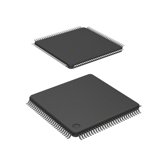
C.1 112-Pin LQFP Package . . . . . . . . . . . . . . . . . . . . . . . . . . . . . . . . . . . . . . . . . . . . . . . . . . . . . . . . . 651
C.2 80-Pin QFP Package . . . . . . . . . . . . . . . . . . . . . . . . . . . . . . . . . . . . . . . . . . . . . . . . . . . . . . . . . . . 652
MC9S12KT256 Data Sheet, Rev. 1.16
16
Freescale Semiconductor
�Chapter 1
MC9S12KT256 Device Overview (MC9S12KT256V1)
1.1
Introduction
The MC9S12KT256 is a 112/80 pin 16-bit Flash-based microcontroller family targeted for high reliability
systems. The MC9S12KT256 has an increased performance in reliability over the life of the product due
to a built-in Error Checking and Correction Code (ECC) in the Flash memory. The program and erase
operations automatically generate six parity bits per word making ECC transparent to the user.
The MC9S12KT256 is comprised of standard on-chip peripherals including a 16-bit central processing
unit (CPU12), 256K bytes of Flash EEPROM, 4K bytes of EEPROM, 12K bytes of RAM, two
asynchronous serial communications interface (SCI), three serial peripheral interface (SPI), IIC-bus, an
8-channel IC/OC timer, two 8-channel 10-bit analog-to-digital converters (ADC), an 8-channel
pulse-width modulator (PWM), three CAN 2.0 A, B software compatible modules, 29 discrete digital I/O
channels (Port A, Port B, Port E and Port K), and 20 discrete digital I/O lines with interrupt and wakeup
capability. The MC9S12KT256 has full 16-bit data paths throughout, however, the external bus can operate
in an 8-bit narrow mode so single 8-bit wide memory can be interfaced for lower cost systems. The
inclusion of a PLL circuit allows power consumption and performance to be adjusted to suit operational
requirements.
1.1.1
•
•
Features
HCS12 Core
— 16-bit HCS12 CPU
– Upward compatible with M68HC11 instruction set
– Interrupt stacking and programmer’s model identical to M68HC11
– Instruction queue
– Enhanced indexed addressing
— MEBI (Multiplexed External Bus Interface)
— MMC (Memory Map and Interface)
— INT (Interrupt Controller)
— DBG (Debugger)
— BDM (Background Debug Mode)
Oscillator
— 4MHz to 16MHz frequency range
— Pierce with amplitude loop control
— Clock monitor
MC9S12KT256 Data Sheet, Rev. 1.16
Freescale Semiconductor
17
�Chapter 1 MC9S12KT256 Device Overview (MC9S12KT256V1)
•
•
•
•
•
•
•
•
Clock and Reset Generator (CRG)
— Phase-locked loop clock frequency multiplier
— Self Clock mode in absence of external clock
— COP watchdog
— Real Time interrupt (RTI)
Memory
— 256K Byte Flash EEPROM
– Internal program/erase voltage generation
– Security and Block Protect bits
– Hamming Error Correction Coding (ECC)
— 4K Byte EEPROM
— 12K Byte static RAM
Single-cycle misaligned word accesses without wait states
Analog-to-Digital Converters (ADC)
— Two 8-channel modules with 10-bit resolution
— External conversion trigger capability
8-channel Timer (TIM)
— Programmable input capture or output compare channels
— Simple PWM mode
— Counter Modulo Reset
— External Event Counting
— Gated Time Accumulation
8-channel Pulse Width Modulator (PWM)
— Programmable period and duty cycle per channel
— 8-bit 8-channel or 16-bit 4-channel
— Edge and center aligned PWM signals
— Emergency shutdown input
Three 1M bit per second, CAN 2.0 A, B software compatible modules
— Five receive and three transmit buffers
— Flexible identifier filter programmable as 2 x 32 bit, 4 x 16 bit or 8 x 8 bit
— Four separate interrupt channels for Rx, Tx, error and wake-up
— Low-pass filter wake-up function
— Loop-back for self test operation
Serial interfaces
— Two asynchronous serial communication interface (SCI)
— Three synchronous serial peripheral interface (SPI)
— Inter-IC Bus (IIC)
Internal 2.5V Regulator
— Input voltage range from 3.15V to 5.5V
MC9S12KT256 Data Sheet, Rev. 1.16
18
Freescale Semiconductor
�Chapter 1 MC9S12KT256 Device Overview (MC9S12KT256V1)
•
•
•
1.1.2
•
•
•
•
— Low power mode capability
— Low Voltage Reset (LVR) and Low Voltage Interrupt (LVI)
20 key wake up inputs
— Rising or falling edge triggered interrupt capability
— Digital filter to prevent short pulses from triggering interrupts
— Programmable pull ups and pull downs
Operating frequency for ambient temperatures (TA -40°C to 125°C)
— 50MHz equivalent to 25MHz Bus Speed
112-Pin LQFP or 80-Pin QFP package
— I/O lines with 3.3V/5V input and drive capability
— 3.3V/5V A/D converter inputs
Modes of Operation
Normal modes
— Normal Single-Chip Mode
— Normal Expanded Wide Mode
— Normal Expanded Narrow Mode
— Emulation Expanded Wide Mode
— Emulation Expanded Narrow Mode
Special Operating Modes
— Special Single-Chip Mode with active Background Debug Mode
— Special Test Mode (Freescale use only)
— Special Peripheral Mode (Freescale use only)
Each of the above modes of operation can be configured for three Low power submodes
— Stop Mode
— Pseudo Stop Mode
— Wait Mode
Secure operation, preventing the unauthorized read and write of the memory contents.
MC9S12KT256 Data Sheet, Rev. 1.16
Freescale Semiconductor
19
�Chapter 1 MC9S12KT256 Device Overview (MC9S12KT256V1)
Table 1-1 shows a feature overview of the MC9S12KT256 members.
Table 1-1. List of MC9S12KT256 members
Device
MC9S12KT256
MC9S12KG256
Temp Options1 Flash RAM EEPROM
C, V, M
C, V, M
256K
256K
12K
12K
4K
4K
Package CAN SCI SPI IIC A/D2 PWM2 TIM2 I/O3
112 LQFP
3
2
3
1
16
8
8
91
112 LQFP
2
2
3
1
16
8
8
91
80 QFP
2
2
3
1
8
7
8
59
1
C: TA = 85˚C, f = 25MHz. V: TA=105˚C, f = 25MHz. M: TA= 125˚C, f = 25MHz
Number of channels
3
I/O is the sum of ports capable to act as digital input or output.
2
Figure 1-1 shows the part number coding based on the package and temperature options for the
MC9S12KT256.
MC9S12 KT256
C FU
Package Option
Temperature Option
Device Title
Controller Family
Temperature Options
C = -40˚C to 85˚C
V = -40˚C to 105˚C
M = -40˚C to 125˚C
Package Options
PV = 112LQFP
FU = 80QFP
Figure 1-1. Order Part number Coding
MC9S12KT256 Data Sheet, Rev. 1.16
20
Freescale Semiconductor
�Chapter 1 MC9S12KT256 Device Overview (MC9S12KT256V1)
MC9S12KT256 Block Diagram
RxCAN
TxCAN
RxCAN
CAN1
TxCAN
RxCAN
CAN4
TxCAN
CAN0
PA7
PA6
PA5
PA4
PA3
PA2
PA1
PA0
PB7
PB6
PB5
PB4
PB3
PB2
PB1
PB0
Multiplexed
Wide Bus
ADDR7
ADDR6
ADDR5
ADDR4
ADDR3
ADDR2
ADDR1
ADDR0
Multiplexed
Narrow Bus
DATA7
DATA6
DATA5
DATA4
DATA3
DATA2
DATA1
DATA0
PTB
ADDR15
ADDR14
ADDR13
ADDR12
ADDR11
ADDR10
ADDR9
ADDR8
DDRB
PTA
DATA15
DATA14
DATA13
DATA12
DATA11
DATA10
DATA9
DATA8
DDRA
DATA7
DATA6
DATA5
DATA4
DATA3
DATA2
DATA1
DATA0
IIC
Internal Logic 2.5V
VDD1,2
VSS1,2
PWM
I/O Driver 3.3V/5V
VDDX
VSSX
OSC/PLL 2.5V
VDDPLL
VSSPLL
Voltage Regulator 3.3V/5V A/D Converter 3.3V/5V
VDDR
Voltage Reference
VSSR
V
SPI1
DDA
VSSA
SPI2
SDA
SCL
KWJ0
KWJ1
KWJ6
KWJ7
PWM0
PWM1
PWM2
PWM3
PWM4
PWM5
PWM6
PWM7
KWP0
KWP1
KWP2
KWP3
KWP4
KWP5
KWP6
KWP7
MISO
MOSI
SCK
SS
MISO
MOSI
SCK
SS
KWH0
KWH1
KWH2
KWH3
KWH4
KWH5
KWH6
KWH7
DDRK
PT0
PT1
PT2
PT3
PT4
PT5
PT6
PT7
PS0
PS1
PS2
PS3
PS4
PS5
PS6
PS7
PM0
PM1
PM2
PM3
PM4
PM5
PM6
PM7
PJ0
PJ1
PJ6
PJ7
PP0
PP1
PP2
PP3
PP4
PP5
PP6
PP7
PH0
PH1
PH2
PH3
PH4
PH5
PH6
PH7
XADDR14
XADDR15
XADDR16
XADDR17
XADDR18
XADDR19
ECS
Signals shown in Bold are not available on n the 80-Pin Package
SPI0
Multiplexed Address/Data Bus
MISO
MOSI
SCK
SS
AD1
SCI1
TEST
PTK
RXD
TXD
RXD
TXD
SCI0
PTT
TIM
DDRT
Breakpoints
XIRQ
Debugger
IRQ
R/W
System
LSTRB
Integration
ECLK
Module
MODA
(SIM)
MODB
NOACC/XCLKS
PK0
PK1
PK2
PK3
PK4
PK5
PK7
PTS
CRG
DDRS
IOC0
IOC1
IOC2
IOC3
IOC4
IOC5
IOC6
IOC7
PLL
PAD08
PAD09
PAD10
PAD11
PAD12
PAD13
PAD14
PAD15
PTM
CPU12
DDRM
Periodic Interrupt
COP Watchdog
Clock Monitor
PIX0
PIX1
PIX2
PIX3
PIX4
PIX5
ECS
VRH
VRL
VDDA
VSSA
PTJ
OSC
AN0
AN1
AN2
AN3
AN4
AN5
AN6
AN7
DDRJ
PE0
PE1
PE2
PE3
PE4
PE5
PE6
PE7
Single-wire BDM
PTE
XTAL
EXTAL
VSSPLL
VDDPLL
XFC
RESET
PPAGE
DDRE
BKGD
Voltage Regulator
VRH
VRL
VDDA
VSSA
PTP
VDDR
VSSR
VREGEN
VDD1,2
VSS1,2
PAD00
PAD01
PAD02
PAD03
PAD04
PAD05
PAD06
PAD07
ATD1
DDRP
AN0
AN1
AN2
AN3
AN4
AN5
AN6
AN7
12K Byte RAM
VRH
VRL
VDDA
VSSA
PTH
4K Byte EEPROM
VRH
VRL
VDDA
VSSA
DDRH
ATD0
Module to
Port Routing
256K Byte Flash EEPROM
AD0
1.1.3
Figure 1-2. MC9S12KT256 Block Diagram
MC9S12KT256 Data Sheet, Rev. 1.16
Freescale Semiconductor
21
�Chapter 1 MC9S12KT256 Device Overview (MC9S12KT256V1)
1.2
Signal Description
MC9S12KT256
112LQFP
84
83
82
81
80
79
78
77
76
75
74
73
72
71
70
69
68
67
66
65
64
63
62
61
60
59
58
57
29
30
31
32
33
34
35
36
37
38
39
40
41
42
43
44
45
46
47
48
49
50
51
52
53
54
55
56
1
2
3
4
5
6
7
8
9
10
11
12
13
14
15
16
17
18
19
20
21
22
23
24
25
26
27
28
VRH
VDDA
PAD15/AN15
PAD07/AN07
PAD14/AN14
PAD06/AN06
PAD13/AN13
PAD05/AN05
PAD12/AN12
PAD04/AN04
PAD11/AN11
PAD03/AN03
PAD10/AN10
PAD02/AN02
PAD09/AN09
PAD01/AN01
PAD08/AN08
PAD00/AN00
VSS2
VDD2
PA7/ADDR15/DATA15
PA6/ADDR14/DATA14
PA5/ADDR13/DATA13
PA4/ADDR12/DATA12
PA3/ADDR11/DATA11
PA2/ADDR10/DATA10
PA1/ADDR9/DATA9
PA0/ADDR8/DATA8
ADDR5/DATA5/PB5
ADDR6/DATA6/PB6
ADDR7/DATA7/PB7
SS2/KWH7/PH7
SCK2/KWH6/PH6
MOSI2/KWH5/PH5
MISO2/KWH4/PH4
XCLKS/NOACC/PE7
MODB/IPIPE1/PE6
MODA/IPIPE0/PE5
ECLK/PE4
VSSR
VDDR
RESET
VDDPLL
XFC
VSSPLL
EXTAL
XTAL
TEST
SS1/KWH3/PH3
SCK1/KWH2/PH2
MOSI1/KWH1/PH1
MISO1/KWH0/PH0
LSTRB/TAGLO/PE3
R/W/PE2
IRQ/PE1
XIRQ/PE0
SS1/PWM3/KWP3/PP3
SCK1/PWM2/KWP2/PP2
MOSI1/PWM1/KWP1/PP1
MISO1/PWM0/KWP0/PP0
XADDR17/PK3
XADDR16/PK2
XADDR15/PK1
XADDR14/PK0
IOC0/PT0
IOC1/PT1
IOC2/PT2
IOC3/PT3
VDD1
VSS1
IOC4/PT4
IOC5/PT5
IOC6/PT6
IOC7/PT7
XADDR19/PK5
XADDR18/PK4
KWJ1/PJ1
KWJ0/PJ0
MODC/TAGHI/BKGD
ADDR0/DATA0/PB0
ADDR1/DATA1/PB1
ADDR2/DATA2/PB2
ADDR3/DATA3/PB3
ADDR4/DATA4/PB4
112
111
110
109
108
107
106
105
104
103
102
101
100
99
98
97
96
95
94
93
92
91
90
89
88
87
86
85
PP4/KWP4/PWM4/MISO2
PP5/KWP5/PWM5/MOSI2
PP6/KWP6/PWM6/SS2
PP7/KWP7/PWM7/SCK2
PK7/ECS
VDDX
VSSX
PM0/RXCAN0
PM1/TXCAN0
PM2/RXCAN1/RXCAN0/MISO0
PM3/TXCAN1/TXCAN0/SS0
PM4/RXCAN0/RXCAN4/MOSI0
PM5/TXCAN0/TXCAN4/SCK0
PJ6/KWJ6/RXCAN4/SDA
PJ7/KWJ7/TXCAN4/SCL
VREGEN
PS7/SS0
PS6/SCK0
PS5/MOSI0
PS4/MISO0
PS3/TXD1
PS2/RXD1
PS1/TXD0
PS0/RXD0
PM6/RXCAN4
PM7/TXCAN4
VSSA
VRL
The MC9S12KT256 is available in a 112-pin low profile quad flat pack (LQFP) and a 80-pin quad flat pack
(QFP). Most pins perform two or more functions, as described in Section 1.2.1, “Signal Properties
Summary”. Figure 1-3 and Figure 1-4 show the pin assignments for different packages.
Signals shown in Bold are not available on the 80-pin package
Figure 1-3. Pin Assignments for 112 LQFP
MC9S12KT256 Data Sheet, Rev. 1.16
22
Freescale Semiconductor
�1
2
3
4
5
6
7
8
9
10
11
12
13
14
15
16
17
18
19
20
MC9S12KT256
80 QFP
60
59
58
57
56
55
54
53
52
51
50
49
48
47
46
45
44
43
42
41
VRH
VDDA
PAD07/AN07
PAD06/AN06
PAD05/AN05
PAD04/AN04
PAD03/AN03
PAD02/AN02
PAD01/AN01
PAD00/AN00
VSS2
VDD2
PA7/ADDR15/DATA15
PA6/ADDR14/DATA14
PA5/ADDR13/DATA13
PA4/ADDR12/DATA12
PA3/ADDR11/DATA11
PA2/ADDR10/DATA10
PA1/ADDR9/DATA9
PA0/ADDR8/DATA8
ADDR5/DATA5/PB5
ADDR6/DATA6/PB6
ADDR7/DATA7/PB7
XCLKS/NOACC/PE7
MODB/IPIPE1/PE6
MODA/IPIPE0/PE5
ECLK/PE4
VSSR
VDDR
RESET
VDDPLL
XFC
VSSPLL
EXTAL
XTAL
TEST
LSTRB/TAGLO/PE3
R/W/PE2
IRQ/PE1
XIRQ/PE0
21
22
23
24
25
26
27
28
29
30
31
32
33
34
35
36
37
38
39
40
PWM3/KWP3/PP3
PWM2/KWP2/PP2
PWM1/KWP1/PP1
PWM0/KWP0/PP0
IOC0/PT0
IOC1/PT1
IOC2/PT2
IOC3/PT3
VDD1
VSS1
IOC4/PT4
IOC5/PT5
IOC6/PT6
IOC7/PT7
MODC/TAGHI/BKGD
ADDR0/DATA0/PB0
ADDR1/DATA1/PB1
ADDR2/DATA2/PB2
ADDR3/DATA3/PB3
ADDR4/DATA4/PB4
80
79
78
77
76
75
74
73
72
71
70
69
68
67
66
65
64
63
62
61
PP4/KWP4/PWM4/MISO2
PP5/KWP5/PWM5/MOSI2
PP7/KWP7/PWM7/SCK2
VDDX
VSSX
PM0/RXCAN0
PM1/TXCAN0
PM2/RXCAN1/RXCAN0/MISO0
PM3/TXCAN1/TXCAN0/SS0
PM4/RXCAN0/RXCAN4/MOSI0
PM5/TXCAN0/TXCAN4/SCK0
PJ6/KWJ6/RXCAN4/SDA
PJ7/KWJ7/TXCAN4/SCL
VREGEN
PS3/TXD1
PS2/RXD1
PS1/TXD0
PS0/RXD0
VSSA
VRL
Chapter 1 MC9S12KT256 Device Overview (MC9S12KT256V1)
Figure 1-4. Pin Assignments for 80 QFP
MC9S12KT256 Data Sheet, Rev. 1.16
Freescale Semiconductor
23
�Chapter 1 MC9S12KT256 Device Overview (MC9S12KT256V1)
1.2.1
Signal Properties Summary
Table 1-2 summarizes the pin functionality. Signals shown in bold are not available in the 80-pin package.
Table 1-3 summarizes the power and ground pins.
Table 1-2. Signal Properties (Sheet 1 of 3)
Pin Name
Function 1
Pin Name
Function 2
Pin Name Pin Name Powered
Function 3 Function 4
by
EXTAL
—
—
—
VDDPLL
Internal Pull
Resistor
Description
CTRL
Reset
State
NA
NA
Oscillator Pins
XTAL
—
—
—
VDDPLL
NA
NA
RESET
—
—
—
VDDR
None
None
TEST
—
—
—
NA
NA
NA
Test Input
VREGEN
—
—
—
VDDX
NA
NA
Voltage Regulator Enable Input
External Reset
XFC
—
—
—
VDDPLL
NA
NA
PLL Loop Filter
BKGD
TAGHI
MODC
—
VDDR
Always Up
Up
Background Debug, Tag High,
Mode Input
PAD[15:8]
AN1[7:0]
—
—
VDDA
None
None
Port AD Input, Analog Inputs of
ATD1
PAD[7:0]
AN0[7:0]
—
—
VDDA
None
None
Port AD Input, Analog Inputs of
ATD0
PA[7:0]
ADDR[15:8]/
DATA[15:8]
—
—
VDDR
PUCR
Disabled Port A I/O, Multiplexed
Address/Data
PB[7:0]
ADDR[7:0]/
DATA[7:0]
—
—
VDDR
PUCR
Disabled Port B I/O, Multiplexed
Address/Data
PE7
NOACC
XCLKS
—
VDDR
PUCR
PE6
IPIPE1
MODB
—
VDDR
While RESET
pin is low:
Down
Port E I/O, Pipe Status, Mode
Input
PE5
IPIPE0
MODA
—
VDDR
While RESET
pin is low:
Down
Port E I/O, Pipe Status, Mode
Input
PE4
ECLK
—
—
VDDR
PUCR
Up
Port E I/O, Bus Clock Output
PE3
LSTRB
TAGLO
—
VDDR
PUCR
Up
Port E I/O, Byte Strobe, Tag Low
PE2
R/W
—
—
VDDR
PUCR
Up
Port E I/O, R/W in expanded
modes
PE1
IRQ
—
—
VDDR
PUCR
Up
Port E Input, Maskable Interrupt
PE0
XIRQ
—
—
VDDR
PUCR
Up
Port E Input, Non Maskable
Interrupt
PH7
KWH7
SS2
—
VDDR
PERH/
PPSH
Disabled Port H I/O, Interrupt, SS of SPI2
PH6
KWH6
SCK2
—
VDDR
PERH/
PPSH
Disabled Port H I/O, Interrupt, SCK of
SPI2
PH5
KWH5
MOSI2
—
VDDR
PERH/
PPSH
Disabled Port H I/O, Interrupt, MOSI of
SPI2
Up
Port E I/O, Access, Clock Select
MC9S12KT256 Data Sheet, Rev. 1.16
24
Freescale Semiconductor
�Chapter 1 MC9S12KT256 Device Overview (MC9S12KT256V1)
Table 1-2. Signal Properties (Sheet 2 of 3)
Pin Name
Function 1
Pin Name
Function 2
Pin Name Pin Name Powered
Function 3 Function 4
by
Internal Pull
Resistor
Description
Reset
State
CTRL
PH4
KWH4
MISO2
—
VDDR
PERH/
PPSH
Disabled Port H I/O, Interrupt, MISO of
SPI2
PH3
KWH3
SS1
—
VDDR
PERH/
PPSH
Disabled Port H I/O, Interrupt, SS of SPI1
PH2
KWH2
SCK1
—
VDDR
PERH/
PPSH
Disabled Port H I/O, Interrupt, SCK of
SPI1
PH1
KWH1
MOSI1
—
VDDR
PERH/
PPSH
Disabled Port H I/O, Interrupt, MOSI of
SPI1
PH0
KWH0
MISO1
—
VDDR
PERH/
PPSH
Disabled Port H I/O, Interrupt, MISO of
SPI1
PJ7
KWJ7
TXCAN4
SCL
VDDX
PERJ/
PPSJ
Up
Port J I/O, Interrupt, TX of CAN4,
SCL of IIC
PJ6
KWJ6
RXCAN4
SDA
VDDX
PERJ/
PPSJ
Up
Port J I/O, Interrupt, RX of CAN4,
SDA of IIC
PJ[1:0]
KWJ[1:0]
—
—
VDDX
PERJ/
PPSJ
Up
Port J I/O, Interrupts
PK7
ECS
ROMCTL
—
VDDX
PUCR
Up
Port K I/O, Emulation Chip
Select,
ROM On Enable
PK[5:0]
XADDR[19:14]
—
—
VDDX
PUCR
Up
Port K I/O, Extended
Addresses
PM7
TXCAN4
—
—
VDDX
PERM/
PPSM
Disabled Port M I/O, CAN4 TX
PM6
RXCAN4
—
—
VDDX
PERM/
PPSM
Disabled Port M I/O, CAN4 RX
PM5
TXCAN0
TXCAN4
SCK0
VDDX
PERM/
PPSM
Disabled Port M I/O, CAN0 TX, CAN4 TX,
SPI0 SCK
PM4
RXCAN0
RXCAN4
MOSI0
VDDX
PERM/
PPSM
Disabled Port M I/O, CAN0 RX, CAN4 RX,
SPI0 MOSI
PM3
TXCAN1
TXCAN0
SS0
VDDX
PERM/
PPSM
Disabled Port M I/O, CAN1 TX, CAN0 TX,
SPI0 SS
PM2
RXCAN1
RXCAN0
MISO0
VDDX
PERM/
PPSM
Disabled Port M I/O, CAN1 RX, CAN0 RX,
SPI0 MISO
PM1
TXCAN0
—
—
VDDX
PERM/
PPSM
Disabled Port M I/O, CAN0 TX
PM0
RXCAN0
—
—
VDDX
PERM/
PPSM
Disabled Port M I/O, CAN0 RX
PP7
KWP7
PWM7
SCK2
VDDX
PERP/
PPSP
Disabled Port P I/O, Interrupt, PWM
Channel 7,
SCK of SPI2
PP6
KWP6
PWM6
SS2
VDDX
PERP/
PPSP
Disabled Port P I/O, Interrupt, PWM
Channel 6, SPI2 SS
MC9S12KT256 Data Sheet, Rev. 1.16
Freescale Semiconductor
25
�Chapter 1 MC9S12KT256 Device Overview (MC9S12KT256V1)
Table 1-2. Signal Properties (Sheet 3 of 3)
Pin Name
Function 1
Pin Name
Function 2
Pin Name Pin Name Powered
Function 3 Function 4
by
Internal Pull
Resistor
Description
CTRL
Reset
State
PP5
KWP5
PWM5
MOSI2
VDDX
PERP/
PPSP
Disabled Port P I/O, Interrupt, PWM
Channel 5,
SPI2 MOSI
PP4
KWP4
PWM4
MISO2
VDDX
PERP/
PPSP
Disabled Port P I/O, Interrupt, PWM
Channel 4, SPI2 MISO
PP3
KWP3
PWM3
SS1
VDDX
PERP/
PPSP
Disabled Port P I/O, Interrupt, PWM
Channel 3, SPI1 SS
PP2
KWP2
PWM2
SCK1
VDDX
PERP/
PPSP
Disabled Port P I/O, Interrupt, PWM
Channel 2, SPI1 SCK
PP1
KWP1
PWM1
MOSI1
VDDX
PERP/
PPSP
Disabled Port P I/O, Interrupt, PWM
Channel 1, SPI1 MOSI
PP0
KWP0
PWM0
MISO1
VDDX
PERP/
PPSP
Disabled Port P I/O, Interrupt, PWM
Channel 0, SPI1 MISO
PS7
SS0
—
—
VDDX
PERS/
PPSS
Up
Port S I/O, SPI0 SS
PS6
SCK0
—
—
VDDX
PERS/
PPSS
Up
Port S I/O, SPI0 SCK
PS5
MOSI0
—
—
VDDX
PERS/
PPSS
Up
Port S I/O, SPI0 MOSI
PS4
MISO0
—
—
VDDX
PERS/
PPSS
Up
Port S I/O, SPI0 MISO
PS3
TXD1
—
—
VDDX
PERS/
PPSS
Up
Port S I/O, SCI1TXD
PS2
RXD1
—
—
VDDX
PERS/
PPSS
Up
Port S I/O, SCI1RXD
PS1
TXD0
—
—
VDDX
PERS/
PPSS
Up
Port S I/O, SCI0 TXD
PS0
RXD0
—
—
VDDX
PERS/
PPSS
Up
Port S I/O, SCI0 RXD
PT[7:0]
IOC[7:0]
—
—
VDDX
Up or
Down
Disabled Port T I/O, Timer channels
MC9S12KT256 Data Sheet, Rev. 1.16
26
Freescale Semiconductor
�Chapter 1 MC9S12KT256 Device Overview (MC9S12KT256V1)
Table 1-3. Power and Ground
Mnemonic
Nominal
Voltage
VDD1 VDD2
2.5 V
VSS1
VSS2
0V
VDDR
3.3/5.0 V
Description
Internal power and ground generated by internal regulator. These also allow an external
source to supply the core VDD/VSS voltages and bypass the internal voltage regulator.
External power and ground, supply to pin drivers and internal voltage regulator.
VSSR
0V
VDDX
3.3/5.0 V
VSSX
0V
VDDA
3.3/5.0 V
VSSA
0V
VRH
3.3/5.0 V
Reference voltage high for the ATD converter.
VRL
0V
Reference voltage low for the ATD converter.
VDDPLL
2.5 V
VSSPLL
0V
External power and ground, supply to pin drivers.
Operating voltage and ground for the analog-to-digital converter and the reference for the
internal voltage regulator, allows the supply voltage to the A/D to be bypassed
independently.
Provides operating voltage and ground for the Phased-Locked Loop. This allows the supply
voltage to the PLL to be bypassed independently. Internal power and ground generated by
internal regulator.
NOTE
All VSS pins must be connected together in the application. Because fast
signal transitions place high, short-duration current demands on the power
supply, use bypass capacitors with high-frequency characteristics and place
them as close to the MCU as possible. Bypass requirements depend on
MCU pin load.
1.2.2
1.2.2.1
Detailed Signal Descriptions
EXTAL, XTAL — Oscillator Pins
EXTAL and XTAL are the crystal driver and external clock pins. On reset all the device clocks are derived
from the EXTAL input frequency. XTAL is the crystal output.
1.2.2.2
RESET — External Reset Pin
An active low bidirectional control signal, it acts as an input to initialize the MCU to a known start-up state,
and an output when an internal MCU function causes a reset.
1.2.2.3
TEST — Test Pin
This input only pin is reserved for test.
NOTE
The TEST pin must be tied to VSS in all applications.
MC9S12KT256 Data Sheet, Rev. 1.16
Freescale Semiconductor
27
�Chapter 1 MC9S12KT256 Device Overview (MC9S12KT256V1)
1.2.2.4
VREGEN — Voltage Regulator Enable Pin
This input only pin enables or disables the on-chip voltage regulator.
1.2.2.5
XFC — PLL Loop Filter Pin
PLL loop filter. Please ask your Freescale representative for the interactive application note to compute
PLL loop filter elements. Any current leakage on this pin must be avoided.
XFC
R
CP
MCU
CS
VDDPLL
VDDPLL
Figure 1-5. PLL Loop Filter Connections
1.2.2.6
BKGD / TAGHI / MODC — Background Debug, Tag High, and Mode Pin
The BKGD/TAGHI/MODC pin is used as a pseudo-open-drain pin for the background debug
communication. In MCU expanded modes of operation when instruction tagging is on, an input low on
this pin during the falling edge of E-clock tags the high half of the instruction word being read into the
instruction queue. It is used as a MCU operating mode select pin during reset. The state of this pin is
latched to the MODC bit at the rising edge of RESET.
1.2.2.7
PAD[15:8] / AN1[7:0] — Port AD Input Pins [15:8]
PAD15 - PAD8 are general purpose input pins and analog inputs of the analog to digital converter with 8
channels (ATD1).
1.2.2.8
PAD[7:0] / AN0[7:0] — Port AD Input Pins [7:0]
PAD7–PAD0 are general purpose input pins and analog inputs of the analog to digital converter with 8
channels (ATD0).
1.2.2.9
PA[7:0] / ADDR[15:8] / DATA[15:8] — Port A I/O Pins
PA7–PA0 are general purpose input or output pins. In MCU expanded modes of operation, these pins are
used for the multiplexed external address and data bus.
1.2.2.10
PB[7:0] / ADDR[7:0] / DATA[7:0] — Port B I/O Pins
PB7–PB0 are general purpose input or output pins. In MCU expanded modes of operation, these pins are
used for the multiplexed external address and data bus.
MC9S12KT256 Data Sheet, Rev. 1.16
28
Freescale Semiconductor
�Chapter 1 MC9S12KT256 Device Overview (MC9S12KT256V1)
1.2.2.11
PE7 / NOACC / XCLKS — Port E I/O Pin 7
PE7 is a general purpose input or output pin. During MCU expanded modes of operation, the NOACC
signal, when enabled, is used to indicate that the current bus cycle is an unused or “free” cycle. This signal
will assert when the CPU is not using the bus.
The XCLKS is an input signal which controls whether a crystal in combination with the internal Loop
Controlled Pierce (low power) oscillator is used or whether Full Swing Pierce oscillator/external clock
circuitry is used. The state of this pin is latched at the rising edge of RESET. If the input is a logic low the
EXTAL pin is configured for an external clock drive or Full Swing Pierce Oscillator. If input is a logic high
a Loop Controlled Pierce oscillator circuit is configured on EXTAL and XTAL. Since this pin is an input
with a pull-up device during reset, if the pin is left floating, the default configuration is a Loop Controlled
Pierce oscillator circuit on EXTAL and XTAL.
Table 1-4. Clock Selection Based on PE7 During Reset
PE7
Description
1
Loop Controlled Pierce Oscillator selected
0
Full Swing Pierce Oscillator or external clock selected
EXTAL
C7
MCU
CRYSTAL OR
CERAMIC
RESONATOR
XTAL
C8
VSSPLL
Figure 1-6. Loop Controlled Pierce Oscillator Connections (PE7 = 1)
EXTAL
C7
MCU
RB
RS*
CRYSTAL OR
CERAMIC
RESONATOR
XTAL
C8
VSSPLL
* Rs can be zero (shorted) when use with higher frequency crystals.
Refer to manufacturer’s data.
Figure 1-7. Full Swing Pierce Oscillator Connections (PE7 = 0)
MC9S12KT256 Data Sheet, Rev. 1.16
Freescale Semiconductor
29
�Chapter 1 MC9S12KT256 Device Overview (MC9S12KT256V1)
EXTAL
CMOS-COMPATIBLE
EXTERNAL OSCILLATOR
(VDDPLL-LEVEL)
MCU
XTAL
NOT CONNECTED
Figure 1-8. External Clock Connections (PE7 = 0)
1.2.2.12
PE6 / MODB / IPIPE1 — Port E I/O Pin 6
PE6 is a general purpose input or output pin. It is used as a MCU operating mode select pin during reset.
The state of this pin is latched to the MODB bit at the rising edge of RESET. This pin is shared with the
instruction queue tracking signal IPIPE1.
1.2.2.13
PE5 / MODA / IPIPE0 — Port E I/O Pin 5
PE5 is a general purpose input or output pin. It is used as a MCU operating mode select pin during reset.
The state of this pin is latched to the MODA bit at the rising edge of RESET. This pin is shared with the
instruction queue tracking signal IPIPE0.
1.2.2.14
PE4 / ECLK — Port E I/O Pin 4
PE4 is a general purpose input or output pin. It can be configured to drive the internal bus clock ECLK.
ECLK can be used as a timing reference.
1.2.2.15
PE3 / LSTRB / TAGLO — Port E I/O Pin 3
PE3 is a general purpose input or output pin. In MCU expanded modes of operation, LSTRB can be used
for the low-byte strobe function to indicate the type of bus access and when instruction tagging is on,
TAGLO is used to tag the low half of the instruction word being read into the instruction queue.
1.2.2.16
PE2 / R/W — Port E I/O Pin 2
PE2 is a general purpose input or output pin. In MCU expanded modes of operations, this pin drives the
read/write output signal for the external bus. It indicates the direction of data on the external bus.
1.2.2.17
PE1 / IRQ — Port E Input Pin 1
PE1 is a general purpose input pin and the maskable interrupt request input that provides a means of
applying asynchronous interrupt requests. This will wake up the MCU from STOP or WAIT mode.
MC9S12KT256 Data Sheet, Rev. 1.16
30
Freescale Semiconductor
�Chapter 1 MC9S12KT256 Device Overview (MC9S12KT256V1)
1.2.2.18
PE0 / XIRQ — Port E Input Pin 0
PE0 is a general purpose input pin and the non-maskable interrupt request input that provides a means of
applying asynchronous interrupt requests. This will wake up the MCU from STOP or WAIT mode.
1.2.2.19
PH7 / KWH7 / SS2 — Port H I/O Pin 7
PH7 is a general purpose input or output pin. It can be configured to generate an interrupt causing the MCU
to exit STOP or WAIT mode. It can be configured as slave select pin SS of the Serial Peripheral Interface 2
(SPI2).
1.2.2.20
PH6 / KWH6 / SCK2 — Port H I/O Pin 6
PH6 is a general purpose input or output pin. It can be configured to generate an interrupt causing the MCU
to exit STOP or WAIT mode. It can be configured as serial clock pin SCK of the Serial Peripheral
Interface 2 (SPI2).
1.2.2.21
PH5 / KWH5 / MOSI2 — Port H I/O Pin 5
PH5 is a general purpose input or output pin. It can be configured to generate an interrupt causing the MCU
to exit STOP or WAIT mode. It can be configured as master output (during master mode) or slave input
pin (during slave mode) MOSI of the Serial Peripheral Interface 2 (SPI2).
1.2.2.22
PH4 / KWH4 / MISO2 — Port H I/O Pin 2
PH4 is a general purpose input or output pin. It can be configured to generate an interrupt causing the MCU
to exit STOP or WAIT mode. It can be configured as master input (during master mode) or slave output
(during slave mode) pin MISO of the Serial Peripheral Interface 2 (SPI2).
1.2.2.23
PH3 / KWH3 / SS1 — Port H I/O Pin 3
PH3 is a general purpose input or output pin. It can be configured to generate an interrupt causing the MCU
to exit STOP or WAIT mode. It can be configured as slave select pin SS of the Serial Peripheral Interface 1
(SPI1).
1.2.2.24
PH2 / KWH2 / SCK1 — Port H I/O Pin 2
PH2 is a general purpose input or output pin. It can be configured to generate an interrupt causing the MCU
to exit STOP or WAIT mode. It can be configured as serial clock pin SCK of the Serial Peripheral
Interface 1 (SPI1).
1.2.2.25
PH1 / KWH1 / MOSI1 — Port H I/O Pin 1
PH1 is a general purpose input or output pin. It can be configured to generate an interrupt causing the MCU
to exit STOP or WAIT mode. It can be configured as master output (during master mode) or slave input
pin (during slave mode) MOSI of the Serial Peripheral Interface 1 (SPI1).
MC9S12KT256 Data Sheet, Rev. 1.16
Freescale Semiconductor
31
�Chapter 1 MC9S12KT256 Device Overview (MC9S12KT256V1)
1.2.2.26
PH0 / KWH0 / MISO1 — Port H I/O Pin 0
PH0 is a general purpose input or output pin. It can be configured to generate an interrupt causing the MCU
to exit STOP or WAIT mode. It can be configured as master input (during master mode) or slave output
(during slave mode) pin MISO of the Serial Peripheral Interface 1 (SPI1).
1.2.2.27
PJ7 / KWJ7 / TXCAN4 / SCL — PORT J I/O Pin 7
PJ7 is a general purpose input or output pin. It can be configured to generate an interrupt causing the MCU
to exit STOP or WAIT mode. It can be configured as the transmit pin TXCAN for the Scalable Controller
Area Network controller 4 (CAN4) or the serial clock pin SCL of the IIC module.
1.2.2.28
PJ6 / KWJ6 / RXCAN4 / SDA — PORT J I/O Pin 6
PJ6 is a general purpose input or output pin. It can be configured to generate an interrupt causing the MCU
to exit STOP or WAIT mode. It can be configured as the receive pin RXCAN for the Scalable Controller
Area Network controller 4 (CAN4) or the serial data pin SDA of the IIC module.
1.2.2.29
PJ[1:0] / KWJ[1:0] — Port J I/O Pins [1:0]
PJ1 and PJ0 are general purpose input or output pins. They can be configured to generate an interrupt
causing the MCU to exit STOP or WAIT mode.
1.2.2.30
PK7 / ECS / ROMCTL — Port K I/O Pin 7
PK7 is a general purpose input or output pin. During MCU expanded modes of operation, this pin is used
as the emulation chip select output (ECS). During MCU expanded modes of operation, this pin is used to
enable the Flash EEPROM memory in the memory map (ROMCTL). At the rising edge of RESET, the
state of this pin is latched to the ROMON bit.
MC9S12KT256 Data Sheet, Rev. 1.16
32
Freescale Semiconductor
�Chapter 1 MC9S12KT256 Device Overview (MC9S12KT256V1)
For all other modes the reset state of the ROMON bit is as follows:
• Special single: ROMCTL = 1
• Normal single: ROMCTL = 1
• Emulation expanded wide: ROMCTL = 0
• Emulation expanded narrow: ROMCTL = 0
• Special test: ROMCTL = 0
• Peripheral test: ROMCTL = 1
1.2.2.31
PK[5:0] / XADDR[19:14] — Port K I/O Pins [5:0]
PK5-PK0 are general purpose input or output pins. In MCU expanded modes of operation, these pins
provide the expanded address XADDR[19:14] for the external bus.
1.2.2.32
PM7 / TXCAN4 — Port M I/O Pin 7
PM7 is a general purpose input or output pin. It can be configured as the transmit pin TXCAN of the
Scalable Controller Area Network controllers 4 (CAN4).
1.2.2.33
PM6 / RXCAN4 — Port M I/O Pin 6
PM6 is a general purpose input or output pin. It can be configured as the receive pin RXCAN of the
Scalable Controller Area Network controllers 4 (CAN4).
1.2.2.34
PM5 / TXCAN0 / TXCAN4 / SCK0 — Port M I/O Pin 5
PM5 is a general purpose input or output pin. It can be configured as the transmit pin TXCAN of the
Scalable Controller Area Network controllers 0 or 4 (CAN0 or CAN4). It can be configured as the serial
clock pin SCK of the Serial Peripheral Interface 0 (SPI0).
1.2.2.35
PM4 / RXCAN0 / RXCAN4/ MOSI0 — Port M I/O Pin 4
PM4 is a general purpose input or output pin. It can be configured as the receive pin RXCAN of the
Scalable Controller Area Network controllers 0 or 4 (CAN0 or CAN4). It can be configured as the master
output (during master mode) or slave input pin (during slave mode) MOSI for the Serial Peripheral
Interface 0 (SPI0).
1.2.2.36
PM3 / TXCAN1 / TXCAN0 / SS0 — Port M I/O Pin 3
PM3 is a general purpose input or output pin. It can be configured as the transmit pin TXCAN of the
Scalable Controller Area Network controllers 1 or 0 (CAN1 or CAN0). It can be configured as the slave
select pin SS of the Serial Peripheral Interface 0 (SPI0).
MC9S12KT256 Data Sheet, Rev. 1.16
Freescale Semiconductor
33
�Chapter 1 MC9S12KT256 Device Overview (MC9S12KT256V1)
1.2.2.37
PM2 / RXCAN1 / RXCAN0 / MISO0 — Port M I/O Pin 2
PM2 is a general purpose input or output pin. It can be configured as the receive pin RXCAN of the
Scalable Controller Area Network controllers 1 or 0 (CAN1 or CAN0). It can be configured as the master
input (during master mode) or slave output pin (during slave mode) MISO for the Serial Peripheral
Interface 0 (SPI0).
1.2.2.38
PM1 / TXCAN0 — Port M I/O Pin 1
PM1 is a general purpose input or output pin. It can be configured as the transmit pin TXCAN of the
Scalable Controller Area Network controller 0 (CAN0).
1.2.2.39
PM0 / RXCAN0 — Port M I/O Pin 0
PM0 is a general purpose input or output pin. It can be configured as the receive pin RXCAN of the
Scalable Controller Area Network controller 0 (CAN0).
1.2.2.40
PP7 / KWP7 / PWM7 / SCK2 — Port P I/O Pin 7
PP7 is a general purpose input or output pin. It can be configured to generate an interrupt causing the MCU
to exit STOP or WAIT mode. It can be configured as Pulse Width Modulator (PWM) channel 7 output. It
can be configured as serial clock pin SCK of the Serial Peripheral Interface 2 (SPI2).
1.2.2.41
PP6 / KWP6 / PWM6 / SS2 — Port P I/O Pin 6
PP6 is a general purpose input or output pin. It can be configured to generate an interrupt causing the MCU
to exit STOP or WAIT mode. It can be configured as Pulse Width Modulator (PWM) channel 6 output. It
can be configured as slave select pin SS of the Serial Peripheral Interface 2 (SPI2).
1.2.2.42
PP5 / KWP5 / PWM5 / MOSI2 — Port P I/O Pin 5
PP5 is a general purpose input or output pin. It can be configured to generate an interrupt causing the MCU
to exit STOP or WAIT mode. It can be configured as Pulse Width Modulator (PWM) channel 5 output. It
can be configured as master output (during master mode) or slave input pin (during slave mode) MOSI of
the Serial Peripheral Interface 2 (SPI2).
1.2.2.43
PP4 / KWP4 / PWM4 / MISO2 — Port P I/O Pin 4
PP4 is a general purpose input or output pin. It can be configured to generate an interrupt causing the MCU
to exit STOP or WAIT mode. It can be configured as Pulse Width Modulator (PWM) channel 4 output. It
can be configured as master input (during master mode) or slave output (during slave mode) pin MISO of
the Serial Peripheral Interface 2 (SPI2).
MC9S12KT256 Data Sheet, Rev. 1.16
34
Freescale Semiconductor
�Chapter 1 MC9S12KT256 Device Overview (MC9S12KT256V1)
1.2.2.44
PP3 / KWP3 / PWM3 / SS1 — Port P I/O Pin 3
PP3 is a general purpose input or output pin. It can be configured to generate an interrupt causing the MCU
to exit STOP or WAIT mode. It can be configured as Pulse Width Modulator (PWM) channel 3 output. It
can be configured as slave select pin SS of the Serial Peripheral Interface 1 (SPI1).
1.2.2.45
PP2 / KWP2 / PWM2 / SCK1 — Port P I/O Pin 2
PP2 is a general purpose input or output pin. It can be configured to generate an interrupt causing the MCU
to exit STOP or WAIT mode. It can be configured as Pulse Width Modulator (PWM) channel 2 output. It
can be configured as serial clock pin SCK of the Serial Peripheral Interface 1 (SPI1).
1.2.2.46
PP1 / KWP1 / PWM1 / MOSI1 — Port P I/O Pin 1
PP1 is a general purpose input or output pin. It can be configured to generate an interrupt causing the MCU
to exit STOP or WAIT mode. It can be configured as Pulse Width Modulator (PWM) channel 1 output. It
can be configured as master output (during master mode) or slave input pin (during slave mode) MOSI of
the Serial Peripheral Interface 1 (SPI1).
1.2.2.47
PP0 / KWP0 / PWM0 / MISO1 — Port P I/O Pin 0
PP0 is a general purpose input or output pin. It can be configured to generate an interrupt causing the MCU
to exit STOP or WAIT mode. It can be configured as Pulse Width Modulator (PWM) channel 0 output. It
can be configured as master input (during master mode) or slave output (during slave mode) pin MISO of
the Serial Peripheral Interface 1 (SPI1).
1.2.2.48
PS7 / SS0 — Port S I/O Pin 7
PS6 is a general purpose input or output pin. It can be configured as the slave select pin SS of the Serial
Peripheral Interface 0 (SPI0).
1.2.2.49
PS6 / SCK0 — Port S I/O Pin 6
PS6 is a general purpose input or output pin. It can be configured as the serial clock pin SCK of the Serial
Peripheral Interface 0 (SPI0).
1.2.2.50
PS5 / MOSI0 — Port S I/O Pin 5
PS5 is a general purpose input or output pin. It can be configured as master output (during master mode)
or slave input pin (during slave mode) MOSI of the Serial Peripheral Interface 0 (SPI0).
1.2.2.51
PS4 / MISO0 — Port S I/O Pin 4
PS4 is a general purpose input or output pin. It can be configured as master input (during master mode) or
slave output pin (during slave mode) MOSI of the Serial Peripheral Interface 0 (SPI0).
MC9S12KT256 Data Sheet, Rev. 1.16
Freescale Semiconductor
35
�Chapter 1 MC9S12KT256 Device Overview (MC9S12KT256V1)
1.2.2.52
PS3 / TXD1 — Port S I/O Pin 3
PS3 is a general purpose input or output pin. It can be configured as the transmit pin TXD of Serial
Communication Interface 1 (SCI1).
1.2.2.53
PS2 / RXD1 — Port S I/O Pin 2
PS2 is a general purpose input or output pin. It can be configured as the receive pin RXD of Serial
Communication Interface 1 (SCI1).
1.2.2.54
PS1 / TXD0 — Port S I/O Pin 1
PS1 is a general purpose input or output pin. It can be configured as the transmit pin TXD of Serial
Communication Interface 0 (SCI0).
1.2.2.55
PS0 / RXD0 — Port S I/O Pin 0
PS0 is a general purpose input or output pin. It can be configured as the receive pin RXD of Serial
Communication Interface 0 (SCI0).
1.2.2.56
PT[7:0] / IOC[7:0] — Port T I/O Pins [7:0]
PT7-PT0 are general purpose input or output pins. They can be configured as input capture or output
compare pins IOC7-IOC0 of the Timer (TIM).
1.2.3
Power Supply Pins
MC9S12KT256 power and ground pins are described below.
NOTE
All VSS pins must be connected together in the application.
1.2.3.1
VDDX,VSSX — Power Supply Pins for I/O Drivers
External power and ground for I/O drivers. Because fast signal transitions place high, short-duration
current demands on the power supply, use bypass capacitors with high-frequency characteristics and place
them as close to the MCU as possible. Bypass requirements depend on how heavily the MCU pins are
loaded.
1.2.3.2
VDDR, VSSR — Power Supply Pins for I/O Drivers & for Internal Voltage
Regulator
External power and ground for I/O drivers and input to the internal voltage regulator. Because fast signal
transitions place high, short-duration current demands on the power supply, use bypass capacitors with
high-frequency characteristics and place them as close to the MCU as possible. Bypass requirements
depend on how heavily the MCU pins are loaded.
MC9S12KT256 Data Sheet, Rev. 1.16
36
Freescale Semiconductor
�Chapter 1 MC9S12KT256 Device Overview (MC9S12KT256V1)
1.2.3.3
VDD1, VDD2, VSS1, VSS2 — Power Supply Pins for Internal Logic
Power is supplied to the MCU through VDD and VSS. Because fast signal transitions place high,
short-duration current demands on the power supply, use bypass capacitors with high-frequency
characteristics and place them as close to the MCU as possible. This 2.5V supply is derived from the
internal voltage regulator. There is no static load on those pins allowed. The internal voltage regulator is
turned off, if VREGEN is tied to ground.
NOTE
No load allowed except for bypass capacitors.
1.2.3.4
VDDA, VSSA — Power Supply Pins for ATD and VREG
VDDA, VSSA are the power supply and ground input pins for the voltage regulator and the analog to
digital converter. It also provides the reference for the internal voltage regulator. This allows the supply
voltage to the ATD and the reference voltage to be bypassed independently.
1.2.3.5
VRH, VRL — ATD Reference Voltage Input Pins
VRH and VRL are the reference voltage input pins for the analog to digital converter.
1.2.3.6
VDDPLL, VSSPLL — Power Supply Pins for PLL
Provides operating voltage and ground for the Oscillator and the Phased-Locked Loop. This allows the
supply voltage to the Oscillator and PLL to be bypassed independently. This 2.5V voltage is generated by
the internal voltage regulator.
NOTE
No load allowed except for bypass capacitors.
MC9S12KT256 Data Sheet, Rev. 1.16
Freescale Semiconductor
37
�Chapter 1 MC9S12KT256 Device Overview (MC9S12KT256V1)
1.3
1.3.1
Memory Map and Register Definition
Device Memory Map
Table 1-5 shows the device register map of the MC9S12KT256 after reset.
Table 1-5. MC9S12KT256 Device Memory Map
Address
Module
Size
0x0000–0x0017
CORE (Ports A, B, E, Modes, Inits, Test)
24
0x0018
Reserved
1
0x0019
Voltage Regulator (VREG)
1
0x001A–0x001B
Device ID register (PARTID)
2
0x001C–0x001F
CORE (MEMSIZ, IRQ, HPRIO)
4
0x0020–0x002F
CORE (DBG)
16
0x0030–0x0033
CORE (PPAGE, Port K)
4
0x0034–0x003F
Clock and Reset Generator (PLL, RTI, COP)
12
0x0040–0x006F
Standard Timer 16-bit 8 channels (TIM)
48
0x0070–0x007F
Reserved
16
0x0080–0x009F
Analog to Digital Converter 10-bit 8 channels (ATD0)
32
0x00A0–0x00C7
Reserved
40
0x00C8–0x00CF
Serial Communications Interface 0 (SCI0)
8
0x00D0–0x00D7
Serial Communications Interface 1 (SCI1)
8
0x00D8–0x00DF
Serial Peripheral Interface 0 (SPI0)
8
0x00E0–0x00E7
Inter Integrated Circuit Bus (IIC)
8
0x00E8–0x00EF
Reserved
8
0x00F0–0x00F7
Serial Peripheral Interface 1 (SPI1)
8
0x00F8–0x00FF
Serial Peripheral Interface 2 (SPI2)
8
0x0100–0x010F
Flash Control Register
16
0x0110- 0x011B
EEPROM Control Register
12
0x011C–0x011F
Reserved
4
0x0120–0x013F
Analog to Digital Converter 10-bit 8 channels (ATD1)
32
0x0140–0x017F
Scalable Controller Area Network 0 (CAN0)
64
0x0180–0x01BF
Scalable Controller Area Network 1 (CAN1)
64
0x01C0–0x023F
Reserved
128
0x0240–0x027F
Port Integration Module (PIM)
64
0x0280–0x02BF
Scalable Controller Area Network 4 (CAN4)
64
0x02C0–0x02E7
Pulse Width Modulator 8-bit 8 channels (PWM)
40
0x02E8–0x03FF
Reserved
280
MC9S12KT256 Data Sheet, Rev. 1.16
38
Freescale Semiconductor
�Chapter 1 MC9S12KT256 Device Overview (MC9S12KT256V1)
Figure 1-9 illustrates the full user configurable device memory map of MC9S12KT256.
0x0000
1K Register Space
0x0000
0x0400
0x03FF
Mappable to any 2K Boundary
0x0000
4K Bytes EEPROM
0x1000
0x0FFF
Mappable to any 4K Boundary
0x1000
12K Bytes RAM
Mappable to any 16K Boundary
0x3FFF and alignable to top or bottom
0x4000
0x4000
0x7FFF
0.5K, 1K, 2K or 4K Protected Sector
16K Fixed Flash EEPROM
0x8000
0x8000
16K Page Window
sixteen * 16K Flash EEPROM Pages
EXT
0xBFFF
0xC000
0xC000
16K Fixed Flash EEPROM
0xFFFF
2K, 4K, 8K or 16K Protected Boot Sector
0xFF00
0xFF00
0xFFFF
VECTORS
VECTORS
VECTORS
NORMAL
SINGLE CHIP
EXPANDED
SPECIAL
SINGLE CHIP
0xFFFF
BDM
(If Active)
The figure shows a useful map, which is not the map out of reset. After reset the map is:
0x0000–0x03FF: Register Space
0x1000–0x3FFF: 12K RAM
0x0000–0x0FFF: 4K EEPROM (1K hidden behind Register Space)
Figure 1-9. MC9S12KT256 Memory Map
MC9S12KT256 Data Sheet, Rev. 1.16
Freescale Semiconductor
39
�Chapter 1 MC9S12KT256 Device Overview (MC9S12KT256V1)
1.3.2
Detailed Register Map
The following tables show the detailed register map of the MC9S12KT256.
0x0000–0x000F MEBI Map 1 of 3 (HCS12 Multiplexed External Bus Interface)
Address
Name
0x0000
PORTA
0x0001
PORTB
0x0002
DDRA
0x0003
DDRB
0x0004
Reserved
0x0005
Reserved
0x0006
Reserved
0x0007
Reserved
0x0008
PORTE
0x0009
DDRE
0x000A
PEAR
0x000B
MODE
0x000C
PUCR
0x000D
RDRIV
0x000E
EBICTL
0x000F
Reserved
Bit 7
R
Bit 7
W
R
Bit 7
W
R
Bit 7
W
R
Bit 7
W
R
0
W
R
0
W
R
0
W
R
0
W
R
Bit 7
W
R
Bit 7
W
R
NOACCE
W
R
MODC
W
R
PUPKE
W
R
RDPK
W
R
0
W
R
0
W
Bit 6
Bit 5
Bit 4
Bit 3
Bit 2
Bit 1
Bit 0
6
5
4
3
2
1
Bit 0
6
5
4
3
2
1
Bit 0
6
5
4
3
2
1
Bit 0
6
5
4
3
2
1
Bit 0
0
0
0
0
0
0
0
0
0
0
0
0
0
0
0
0
0
0
0
0
0
0
0
0
0
0
0
0
6
5
4
3
2
Bit 1
Bit 0
6
5
4
3
Bit 2
0
0
PIPOE
NECLK
LSTRE
RDWE
0
0
EMK
EME
PUPBE
PUPAE
RDPB
RDPA
0
MODB
MODA
0
0
0
0
0
0
0
0
0
IVIS
0
0
0
0
0
0
0
0
0
0
0
0
0
PUPEE
RDPE
ESTR
0
MC9S12KT256 Data Sheet, Rev. 1.16
40
Freescale Semiconductor
�Chapter 1 MC9S12KT256 Device Overview (MC9S12KT256V1)
0x0010–0x0014 MMC Map 1 of 4 (HCS12 Module Mapping Control)
Address
Name
0x0010
INITRM
0x0011
INITRG
0x0012
INITEE
0x0013
MISC
0x0014
Reserved
R
W
R
W
R
W
R
W
R
W
Bit 7
Bit 6
Bit 5
Bit 4
Bit 3
RAM15
RAM14
RAM13
RAM12
RAM11
REG14
REG13
REG12
REG11
EE15
EE14
EE13
EE12
EE11
0
0
0
0
0
0
0
0
Bit 2
Bit 1
Bit 0
0
0
0
0
0
0
EXSTR1
EXSTR0
ROMHM
ROMON
0
0
0
0
0
Bit 4
Bit 3
Bit 2
Bit 1
Bit 0
WRINT
ADR3
ADR2
ADR1
ADR0
INT8
INT6
INT4
INT2
INT0
RAMHAL
0
EEON
0x0015–0x0016 INT Map 1 of 2 (HCS12 Interrupt)
Address
Name
0x0015
ITCR
0x0016
ITEST
R
W
R
W
Bit 7
Bit 6
Bit 5
0
0
0
INTE
INTC
INTA
0x0017–0x0017 MMC Map 2 of 4 (HCS12 Module Mapping Control)
Address
0x0017
Name
Reserved
R
W
Bit 7
Bit 6
Bit 5
Bit 4
Bit 3
Bit 2
Bit 1
Bit 0
0
0
0
0
0
0
0
0
0x0018–0x0018 Miscellaneous Peripherals (Device Guide)
Address
Name
0x0018
Reserved
R
W
Bit 7
Bit 6
Bit 5
Bit 4
Bit 3
Bit 2
Bit 1
Bit 0
0
0
0
0
0
0
0
0
Bit 1
Bit 0
LVIE
LVIF
0x0019–0x0019 VREG3V3 (Voltage Regulator)
Address
0x0019
Name
VREGCTRL
R
W
Bit 7
Bit 6
Bit 5
Bit 4
Bit 3
Bit 2
0
0
0
0
0
LVDS
0x001A–0x001B Miscellaneous Peripherals (Device Guide)
Address
Name
0x001A
PARTIDH
0x001B
PARTIDL
R
W
R
W
Bit 7
Bit 6
Bit 5
Bit 4
Bit 3
Bit 2
Bit 1
Bit 0
ID15
ID14
ID13
ID12
ID11
ID10
ID9
ID8
ID7
ID6
ID5
ID4
ID3
ID2
ID1
ID0
MC9S12KT256 Data Sheet, Rev. 1.16
Freescale Semiconductor
41
�Chapter 1 MC9S12KT256 Device Overview (MC9S12KT256V1)
0x001C–0x001D MMC Map 3 of 4 (HCS12 Module Mapping Control, Device Guide)
Address
Name
0x001C
MEMSIZ0
0x001D
MEMSIZ1
Bit 7
R reg_sw0
W
R rom_sw1
W
Bit 6
Bit 5
Bit 4
Bit 3
Bit 2
Bit 1
Bit 0
0
eep_sw1
eep_sw0
0
ram_sw2
ram_sw1
ram_sw0
rom_sw0
0
0
0
0
pag_sw1
pag_sw0
0x001E–0x001E MEBI Map 2 of 3 (HCS12 Multiplexed External Bus Interface)
Address
Name
0x001E
INTCR
R
W
Bit 7
Bit 6
IRQE
IRQEN
Bit 5
Bit 4
Bit 3
Bit 2
Bit 1
Bit 0
0
0
0
0
0
0
Bit 0
0x001F–0x001F INT Map 2 of 2 (HCS12 Interrupt)
Address
0x001F
Name
HPRIO
R
W
Bit 7
Bit 6
Bit 5
Bit 4
Bit 3
Bit 2
Bit 1
PSEL7
PSEL6
PSEL5
PSEL4
PSEL3
PSEL2
PSEL1
Bit 5
Bit 4
Bit 3
Bit 2
Bit 1
TRGSEL
BEGIN
DBGBRK
CF
0
Bit 13
Bit 12
Bit 11
Bit 10
Bit 9
Bit 8
Bit 5
Bit 4
Bit 3
Bit 2
Bit 1
Bit 0
0
0x0020–0x002F DBG Map 1 of 1 (HCS12 Debug)
Address
0x0020
0x0021
0x0022
0x0023
0x0024
0x0025
0x0026
0x0027
0x0028
0x0029
0x002A
0x002B
Name
DBGC1
—
DBGSC
—
DBGTBH
—
DBGTBL
—
DBGCNT
—
DBGCCX
—
DBGCCH
—
DBGCCL
—
DBGC2
BKPCT0
DBGC3
BKPCT1
DBGCAX
BKP0X
DBGCAH
BKP0H
Bit 7
Bit 6
R
DBGEN
ARM
W
R
AF
BF
W
R
Bit 15
Bit 14
W
R
Bit 7
Bit 6
W
R
TBF
0
W
R
PAGSEL
W
R
Bit 15
14
W
R
Bit 7
6
W
R
BKABEN
FULL
W
R
BKAMBH BKAMBL
W
R
PAGSEL
W
R
Bit 15
14
W
0
Bit 0
CAPMOD
TRG
CNT
EXTCMP
13
12
11
10
9
Bit 8
5
4
3
2
1
Bit 0
BDM
TAGAB
BKCEN
TAGC
RWCEN
RWC
BKBMBH
BKBMBL
RWAEN
RWA
RWBEN
RWB
9
Bit 8
EXTCMP
13
12
11
10
MC9S12KT256 Data Sheet, Rev. 1.16
42
Freescale Semiconductor
�Chapter 1 MC9S12KT256 Device Overview (MC9S12KT256V1)
0x0020–0x002F DBG Map 1 of 1 (HCS12 Debug) (continued)
Address
0x002C
0x002D
0x002E
0x002F
Name
DBGCAL
BKP0L
DBGCBX
BKP1X
DBGCBH
BKP1H
DBGCBL
BKP1L
R
W
R
W
R
W
R
W
Bit 7
Bit 6
Bit 5
Bit 4
Bit 3
Bit 2
Bit 1
Bit 0
Bit 7
6
5
4
3
2
1
Bit 0
PAGSEL
EXTCMP
Bit 15
14
13
12
11
10
9
Bit 8
Bit 7
6
5
4
3
2
1
Bit 0
0x0030–0x0031 MMC Map 4 of 4 (HCS12 Module Mapping Control)
Address
Name
0x0030
PPAGE
0x0031
Reserved
R
W
R
W
Bit 7
Bit 6
0
0
0
0
Bit 5
Bit 4
Bit 3
Bit 2
Bit 1
Bit 0
PIX5
PIX4
PIX3
PIX2
PIX1
PIX0
0
0
0
0
0
0
0x0032–0x0033 MEBI Map 3 of 3 (HCS12 Multiplexed External Bus Interface)
Address
Name
0x0032
PORTK
0x0033
DDRK
R
W
R
W
Bit 7
Bit 6
Bit 5
Bit 4
Bit 3
Bit 2
Bit 1
Bit 0
Bit 7
6
5
4
3
2
1
Bit 0
Bit 7
6
5
4
3
2
1
Bit 0
Bit 5
Bit 4
Bit 3
Bit 2
Bit 1
Bit 0
SYN5
SYN4
SYN3
SYN2
SYN1
SYN0
REFDV3
REFDV2
REFDV1
REFDV0
TOUT3
TOUT2
TOUT1
TOUT0
LOCK
TRACK
0
0
PLLWAI
CWAI
RTIWAI
COPWAI
PRE
PCE
SCME
RTR2
RTR1
RTR0
0x0034–0x003F CRG (Clock and Reset Generator)
Address
Name
0x0034
SYNR
0x0035
REFDV
0x0036
CTFLG
TEST ONLY
0x0037
CRGFLG
0x0038
CRGINT
0x0039
CLKSEL
0x003A
PLLCTL
0x003B
RTICTL
R
W
R
W
R
W
R
W
R
W
R
W
R
W
R
W
Bit 7
Bit 6
0
0
0
0
0
0
TOUT7
TOUT6
TOUT5
TOUT4
RTIF
PROF
0
LOCKIF
0
0
PLLSEL
PSTP
SYSWAI
ROAWAI
CME
PLLON
AUTO
ACQ
RTR6
RTR5
RTR4
RTIE
0
LOCKIE
0
RTR3
SCMIF
SCMIE
SCM
0
MC9S12KT256 Data Sheet, Rev. 1.16
Freescale Semiconductor
43
�Chapter 1 MC9S12KT256 Device Overview (MC9S12KT256V1)
0x0034–0x003F CRG (Clock and Reset Generator) (continued)
Address
Name
0x003C
COPCTL
0x003D
FORBYP
TEST ONLY
0x003E
CTCTL
TEST ONLY
0x003F
ARMCOP
R
W
R
W
R
W
R
W
Bit 7
Bit 6
Bit 5
Bit 4
Bit 3
WCOP
RSBCK
0
0
0
RTIBYP
COPBYP
TCTL7
TCTL6
TCTL5
0
Bit 7
0
6
0
5
0
Bit 2
Bit 1
Bit 0
CR2
CR1
CR0
0
0
TCTL4
TCLT3
TCTL2
TCTL1
TCTL0
0
4
0
3
0
2
0
1
0
Bit 0
PLLBYP
FCM
0
0x0040–0x006FTIM (Timer 16 Bit 8 Channels) (Sheet 1 of 3)
Address
Name
0x0040
TIOS
0x0041
CFORC
0x0042
OC7M
0x0043
OC7D
0x0044
TCNT (hi)
0x0045
TCNT (lo)
0x0046
TSCR1
0x0047
TTOV
0x0048
TCTL1
0x0049
TCTL2
0x004A
TCTL3
0x004B
TCTL4
0x004C
TIE
0x004D
TSCR2
0x004E
TFLG1
0x004F
TFLG2
R
W
R
W
R
W
R
W
R
W
R
W
R
W
R
W
R
W
R
W
R
W
R
W
R
W
R
W
R
W
R
W
Bit 7
Bit 6
Bit 5
Bit 4
Bit 3
Bit 2
Bit 1
Bit 0
IOS7
IOS6
IOS5
IOS4
IOS3
IOS2
IOS1
IOS0
0
FOC7
0
FOC6
0
FOC5
0
FOC4
0
FOC3
0
FOC2
0
FOC1
0
FOC0
OC7M7
OC7M6
OC7M5
OC7M4
OC7M3
OC7M2
OC7M1
OC7M0
OC7D7
OC7D6
OC7D5
OC7D4
OC7D3
OC7D2
OC7D1
OC7D0
Bit 15
14
13
12
11
10
9
Bit 8
Bit 7
6
5
4
3
2
1
Bit 0
TEN
TSWAI
TSFRZ
TFFCA
0
0
0
0
TOV7
TOV6
TOV5
TOV4
TOV3
TOV2
TOV1
TOV0
OM7
OL7
OM6
OL6
OM5
OL5
OM4
OL4
OM3
OL3
OM2
OL2
OM1
OL1
OM0
OL0
EDG7B
EDG7A
EDG6B
EDG6A
EDG5B
EDG5A
EDG4B
EDG4A
EDG3B
EDG3A
EDG2B
EDG2A
EDG1B
EDG1A
EDG0B
EDG0A
C7I
C6I
C5I
C4I
C3I
C2I
C1I
C0I
0
0
0
TCRE
PR2
PR1
PR0
C6F
C5F
C4F
C3F
C2F
C1F
C0F
0
0
0
0
0
0
0
TOI
C7F
TOF
MC9S12KT256 Data Sheet, Rev. 1.16
44
Freescale Semiconductor
�Chapter 1 MC9S12KT256 Device Overview (MC9S12KT256V1)
0x0040–0x006FTIM (Timer 16 Bit 8 Channels) (Sheet 2 of 3)
Address
Name
0x0050
TC0 (hi)
0x0051
TC0 (lo)
0x0052
TC1 (hi)
0x0053
TC1 (lo)
0x0054
TC2 (hi)
0x0055
TC2 (lo)
0x0056
TC3 (hi)
0x0057
TC3 (lo)
0x0058
TC4 (hi)
0x0059
TC4 (lo)
0x005A
TC5 (hi)
0x005B
TC5 (lo)
0x005C
TC6 (hi)
0x005D
TC6 (lo)
0x005E
TC7 (hi)
0x005F
TC7 (lo)
0x0060
PACTL
0x0061
PAFLG
0x0062
PACNT (hi)
0x0063
PACNT (lo)
0x0064
Reserved
0x0065
Reserved
0x0066
Reserved
R
W
R
W
R
W
R
W
R
W
R
W
R
W
R
W
R
W
R
W
R
W
R
W
R
W
R
W
R
W
R
W
R
W
R
W
R
W
R
W
R
W
R
W
R
W
Bit 7
Bit 6
Bit 5
Bit 4
Bit 3
Bit 2
Bit 1
Bit 0
Bit 15
14
13
12
11
10
9
Bit 8
Bit 7
6
5
4
3
2
1
Bit 0
Bit 15
14
13
12
11
10
9
Bit 8
Bit 7
6
5
4
3
2
1
Bit 0
Bit 15
14
13
12
11
10
9
Bit 8
Bit 7
6
5
4
3
2
1
Bit 0
Bit 15
14
13
12
11
10
9
Bit 8
Bit 7
6
5
4
3
2
1
Bit 0
Bit 15
14
13
12
11
10
9
Bit 8
Bit 7
6
5
4
3
2
1
Bit 0
Bit 15
14
13
12
11
10
9
Bit 8
Bit 7
6
5
4
3
2
1
Bit 0
Bit 15
14
13
12
11
10
9
Bit 8
Bit 7
6
5
4
3
2
1
Bit 0
Bit 15
14
13
12
11
10
9
Bit 8
Bit 7
6
5
4
3
2
1
Bit 0
PAEN
PAMOD
PEDGE
CLK1
CLK0
PAOVI
PAI
0
0
0
0
0
0
PAOVF
PAIF
Bit 7
6
5
4
3
2
1
Bit 0
Bit 7
6
5
4
3
2
1
Bit 0
0
0
0
0
0
0
0
0
0
0
0
0
0
0
0
0
0
0
0
0
0
0
0
0
0
MC9S12KT256 Data Sheet, Rev. 1.16
Freescale Semiconductor
45
�Chapter 1 MC9S12KT256 Device Overview (MC9S12KT256V1)
0x0040–0x006FTIM (Timer 16 Bit 8 Channels) (Sheet 3 of 3)
Address
Name
0x0067
Reserved
0x0068
Reserved
0x0069
Reserved
0x006A
Reserved
0x006B
Reserved
0x006C
Reserved
0x006D
Reserved
0x006E
Reserved
0x006F
Reserved
R
W
R
W
R
W
R
W
R
W
R
W
R
W
R
W
R
W
Bit 7
Bit 6
Bit 5
Bit 4
Bit 3
Bit 2
Bit 1
Bit 0
0
0
0
0
0
0
0
0
0
0
0
0
0
0
0
0
0
0
0
0
0
0
0
0
0
0
0
0
0
0
0
0
0
0
0
0
0
0
0
0
0
0
0
0
0
0
0
0
0
0
0
0
0
0
0
0
0
0
0
0
0
0
0
0
0
0
0
0
0
0
0
0
Bit 7
Bit 6
Bit 5
Bit 4
Bit 3
Bit 2
Bit 1
Bit 0
0
0
0
0
0
0
0
0
Bit 2
Bit 1
Bit 0
WRAP2
WRAP1
WRAP0
0x0070–0x007FReserved Space
Address
Name
0x0070–
0x007F
Reserved
R
W
0x0080–0x009F ATD0 (Analog to Digital Converter 10 Bit 8 Channel)
Address
Name
0x0080
ATD0CTL0
0x0081
ATD0CTL1
0x0082
ATD0CTL2
0x0083
ATD0CTL3
0x0084
ATD0CTL4
0x0085
ATD0CTL5
0x0086
ATD0STAT0
0x0087
Reserved
Bit 7
R
0
W
R
ETRIGSEL
W
R
ADPU
W
R
0
W
R
SRES8
W
R
DJM
W
R
SCF
W
R
0
W
Bit 6
Bit 5
Bit 4
Bit 3
0
0
0
0
0
0
0
0
AFFC
AWAI
ETRIGLE
ETRIGP
ETRIG
ASCIE
S8C
S4C
S2C
S1C
FIFO
FRZ1
FRZ0
SMP1
SMP0
PRS4
PRS3
PRS2
PRS1
PRS0
DSGN
SCAN
MULT
CC
CB
CA
ETORF
FIFOR
0
CC2
CC1
CC0
0
0
0
0
0
0
0
0
0
ETRIGCH2 ETRIGCH1 ETRIGCH0
ASCIF
MC9S12KT256 Data Sheet, Rev. 1.16
46
Freescale Semiconductor
�Chapter 1 MC9S12KT256 Device Overview (MC9S12KT256V1)
0x0080–0x009F ATD0 (Analog to Digital Converter 10 Bit 8 Channel) (continued)
Address
Name
0x0088
ATD0TEST0
0x0089
ATD0TEST1
0x008A
Reserved
0x008B
ATD0STAT1
0x008C
Reserved
0x008D
ATD0DIEN
0x008E
Reserved
0x008F
PORTAD0
0x0090
ATD0DR0H
0x0091
ATD0DR0L
0x0092
ATD0DR1H
0x0093
ATD0DR1L
0x0094
ATD0DR2H
0x0095
ATD0DR2L
0x0096
ATD0DR3H
0x0097
ATD0DR3L
0x0098
ATD0DR4H
0x0099
ATD0DR4L
0x009A
ATD0DR5H
0x009B
ATD0DR5L
0x009C
ATD0DR6H
R
W
R
W
R
W
R
W
R
W
R
W
R
W
R
W
R
W
R
W
R
W
R
W
R
W
R
W
R
W
R
W
R
W
R
W
R
W
R
W
R
W
Bit 7
Bit 6
Bit 5
Bit 4
Bit 3
Bit 2
Bit 1
Bit 0
0
0
0
0
0
0
0
0
0
0
0
0
0
0
0
0
0
0
0
0
0
CCF7
CCF6
CCF5
CCF4
CCF3
CCF2
CCF1
CCF0
0
0
0
0
0
0
0
0
IEN7
IEN6
IEN5
IEN4
IEN3
IEN2
IEN1
IEN0
0
0
0
0
0
0
0
0
PTAD7
PTAD6
PTAD5
PTAD4
PTAD3
PTAD2
PTAD1
PTAD0
Bit 15
14
13
12
11
10
9
Bit 8
Bit 7
Bit 6
0
0
0
0
0
0
Bit 15
14
13
12
11
10
9
Bit 8
Bit 7
Bit 6
0
0
0
0
0
0
Bit 15
14
13
12
11
10
9
Bit 8
Bit 7
Bit 6
0
0
0
0
0
0
Bit 15
14
13
12
11
10
9
Bit 8
Bit 7
Bit 6
0
0
0
0
0
0
Bit 15
14
13
12
11
10
9
Bit 8
Bit 7
Bit 6
0
0
0
0
0
0
Bit 15
14
13
12
11
10
9
Bit 8
Bit 7
Bit 6
0
0
0
0
0
0
Bit 15
14
13
12
11
10
9
Bit 8
0
0
SC
MC9S12KT256 Data Sheet, Rev. 1.16
Freescale Semiconductor
47
�Chapter 1 MC9S12KT256 Device Overview (MC9S12KT256V1)
0x0080–0x009F ATD0 (Analog to Digital Converter 10 Bit 8 Channel) (continued)
Address
Name
0x009D
ATD0DR6L
0x009E
ATD0DR7H
0x009F
ATD0DR7L
R
W
R
W
R
W
Bit 7
Bit 6
Bit 5
Bit 4
Bit 3
Bit 2
Bit 1
Bit 0
Bit 7
Bit 6
0
0
0
0
0
0
Bit 15
14
13
12
11
10
9
Bit 8
Bit 7
Bit 6
0
0
0
0
0
0
0x00A0–0x00C7
Address
Name
0x00A0–
0x00C7
Reserved
R
W
Reserved space
Bit 7
Bit 6
Bit 5
Bit 4
Bit 3
Bit 2
Bit 1
Bit 0
0
0
0
0
0
0
0
0
Bit 4
Bit 3
Bit 2
Bit 1
Bit 0
SBR12
SBR11
SBR10
SBR9
SBR8
0x00C8–0x00CF SCI0 (Asynchronous Serial Interface)
Address
Name
0x00C8
SCI0BDH
0x00C9
SCI0BDL
0x00CA
SCI0CR1
0x00CB
SCI0CR2
0x00CC
SCI0SR1
0x00CD
SCI0SR2
0x00CE
SCI0DRH
0x00CF
SCI0DRL
R
W
R
W
R
W
R
W
R
W
R
W
R
W
R
W
Bit 7
Bit 6
Bit 5
0
0
0
SBR7
SBR6
SBR5
SBR4
SBR3
SBR2
SBR1
SBR0
LOOPS
SCISWAI
RSRC
M
WAKE
ILT
PE
PT
TIE
TCIE
RIE
ILIE
TE
RE
RWU
SBK
TDRE
TC
RDRF
IDLE
OR
NF
FE
PF
0
0
0
0
0
BRK13
TXDIR
0
0
0
0
0
0
R5
T5
R4
T4
R3
T3
R2
T2
R1
T1
R0
T0
Bit 4
Bit 3
Bit 2
Bit 1
Bit 0
SBR12
SBR11
SBR10
SBR9
SBR8
R8
R7
T7
T8
R6
T6
RAF
0x00D0–0x00D7 SCI1 (Asynchronous Serial Interface)
Address
Name
0x00D0
SCI1BDH
0x00D1
SCI1BDL
0x00D2
SCI1CR1
0x00D3
SCI1CR2
R
W
R
W
R
W
R
W
Bit 7
Bit 6
Bit 5
0
0
0
SBR7
SBR6
SBR5
SBR4
SBR3
SBR2
SBR1
SBR0
LOOPS
SCISWAI
RSRC
M
WAKE
ILT
PE
PT
TIE
TCIE
RIE
ILIE
TE
RE
RWU
SBK
MC9S12KT256 Data Sheet, Rev. 1.16
48
Freescale Semiconductor
�Chapter 1 MC9S12KT256 Device Overview (MC9S12KT256V1)
0x00D0–0x00D7 SCI1 (Asynchronous Serial Interface)
Address
Name
0x00D4
SCI1SR1
0x00D5
SCI1SR2
0x00D6
SCI1DRH
0x00D7
SCI1DRL
R
W
R
W
R
W
R
W
Bit 7
Bit 6
Bit 5
Bit 4
Bit 3
Bit 2
Bit 1
Bit 0
TDRE
TC
RDRF
IDLE
OR
NF
FE
PF
0
0
0
0
0
BRK13
TXDIR
0
0
0
0
0
0
R5
T5
R4
T4
R3
T3
R2
T2
R1
T1
R0
T0
R8
T8
R7
T7
R6
T6
RAF
0x00D8–0x00DF SPI0 (Serial Peripheral Interface)
Address
Name
0x00D8
SPI0CR1
0x00D9
SPI0CR2
0x00DA
SPI0BR
0x00DB
SPI0SR
0x00DC
Reserved
0x00DD
SPI0DR
0x00DE
Reserved
0x00DF
Reserved
R
W
R
W
R
W
R
W
R
W
R
W
R
W
R
W
Bit 7
Bit 6
Bit 5
Bit 4
Bit 3
Bit 2
Bit 1
Bit 0
SPIE
SPE
SPTIE
MSTR
CPOL
CPHA
SSOE
LSBFE
0
0
0
MODFEN
BIDIROE
SPISWAI
SPC0
SPPR2
SPPR1
SPPR0
SPR2
SPR1
SPR0
SPIF
0
SPTEF
MODF
0
0
0
0
0
0
0
0
0
0
0
0
Bit 7
6
5
4
3
2
1
Bit 0
0
0
0
0
0
0
0
0
0
0
0
0
0
0
0
0
Bit 7
Bit 6
Bit 5
Bit 4
Bit 3
Bit 2
Bit 1
Bit 0
ADR7
ADR6
ADR5
ADR4
ADR3
ADR2
ADR1
0
IBC7
IBC6
IBC5
IBC4
IBC3
IBC2
IBC1
IBC0
IBEN
IBIE
MS/SL
TX/RX
TXAK
0
TCF
IAAS
IBB
0
0
RSTA
SRW
D7
D6
D5
D3
D2
0
0
0
0x00E0–0x00E7 IIC (Inter IC Bus)
Address
Name
0x00E0
IBAD
0x00E1
IBFD
0x00E2
IBCR
0x00E3
IBSR
0x00E4
IBDR
R
W
R
W
R
W
R
W
R
W
IBAL
D4
IBIF
D1
IBSWAI
RXAK
D0
MC9S12KT256 Data Sheet, Rev. 1.16
Freescale Semiconductor
49
�Chapter 1 MC9S12KT256 Device Overview (MC9S12KT256V1)
0x00E0–0x00E7 IIC (Inter IC Bus)
Address
Name
0x00E5
Reserved
0x00E6
Reserved
0x00E7
Reserved
R
W
R
W
R
W
Bit 7
Bit 6
Bit 5
Bit 4
Bit 3
Bit 2
Bit 1
Bit 0
0
0
0
0
0
0
0
0
0
0
0
0
0
0
0
0
0
0
0
0
0
0
0
0
Bit 7
Bit 6
Bit 5
Bit 4
Bit 3
Bit 2
Bit 1
Bit 0
0
0
0
0
0
0
0
0
0x00E8–0x00EF Reserved Space
Address
Name
0x00E8–
0x00EF
Reserved
R
W
0x00F0–0x00F7 SPI1 (Serial Peripheral Interface)
Address
Name
0x00F0
SPI1CR1
0x00F1
SPI1CR2
0x00F2
SPI1BR
0x00F3
SPI1SR
0x00F4
Reserved
0x00F5
SPI1DR
0x00F6
Reserved
0x00F7
Reserved
R
W
R
W
R
W
R
W
R
W
R
W
R
W
R
W
Bit 7
Bit 6
Bit 5
Bit 4
Bit 3
Bit 2
Bit 1
Bit 0
SPIE
SPE
SPTIE
MSTR
CPOL
CPHA
SSOE
LSBFE
0
0
0
MODFEN
BIDIROE
SPISWAI
SPC0
SPPR2
SPPR1
SPPR0
SPR2
SPR1
SPR0
SPIF
0
SPTEF
MODF
0
0
0
0
0
0
0
0
0
0
0
0
Bit 7
6
5
4
3
2
1
Bit 0
0
0
0
0
0
0
0
0
0
0
0
0
0
0
0
0
0
0
0
0x00F8–0x00FF SPI2 (Serial Peripheral Interface)
Address
Name
0x00F8
SPI2CR1
0x00F9
SPI2CR2
0x00FA
SPI2BR
0x00FB
SPI2SR
R
W
R
W
R
W
R
W
Bit 7
Bit 6
Bit 5
Bit 4
Bit 3
Bit 2
Bit 1
Bit 0
SPIE
SPE
SPTIE
MSTR
CPOL
CPHA
SSOE
LSBFE
0
0
0
MODFEN
BIDIROE
SPISWAI
SPC0
SPPR2
SPPR1
SPPR0
SPR2
SPR1
SPR0
0
SPTEF
MODF
0
0
0
0
SPIF
0
0
0
MC9S12KT256 Data Sheet, Rev. 1.16
50
Freescale Semiconductor
�Chapter 1 MC9S12KT256 Device Overview (MC9S12KT256V1)
0x00F8–0x00FF SPI2 (Serial Peripheral Interface)
Address
Name
0x00FC
Reserved
0x00FD
SPI2DR
0x00FE
Reserved
0x00FF
Reserved
R
W
R
W
R
W
R
W
Bit 7
Bit 6
Bit 5
Bit 4
Bit 3
Bit 2
Bit 1
Bit 0
0
0
0
0
0
0
0
0
Bit 7
6
5
4
3
2
1
Bit 0
0
0
0
0
0
0
0
0
0
0
0
0
0
0
0
0
Bit 5
Bit 4
Bit 3
Bit 2
Bit 1
Bit 0
FDIV5
FDIV4
FDIV3
FDIV2
FDIV1
FDIV0
RNV5
RNV4
RNV3
RNV2
WRALL
FDFD
0x0100–0x010F Flash Control Register
Address
Name
0x0100
FCLKDIV
0x0101
FSEC
0x0102
FTSTMOD
0x0103
FCNFG
0x0104
FPROT
0x0105
FSTAT
0x0106
FCMD
0x0107
FCTL
0x0108
FADDRHI
0x0109
FADDRLO
0x010A
FDATAHI
0x010B
FDATALO
0x010C
Reserved
0x010D
Reserved
0x010E
Reserved
0x010F
Reserved
Bit 7
Bit 6
R FDIVLD
PRDIV8
W
R
KEYEN
W
R
0
0
W
R
CBEIE
CCIE
W
R
RNV6
FPOPEN
W
R
CCIF
CBEIF
W
R
0
W
R
NV7
NV6
W
R
W
R
W
R
W
R
W
R
0
0
W
R
0
0
W
R
0
0
W
R
0
0
W
0
KEYACC
0
DFDIE
FPHDIS
PVIOL
FPHS
ACCERR
SEC
0
0
0
0
FPLDIS
DFDIF
0
BKSEL
FPLS
BLANK
0
0
NV2
NV1
NV0
CMDB
NV5
NV4
NV3
FADDRHI
FADDRLO
FDATAHI
FDATALO
0
0
0
0
0
0
0
0
0
0
0
0
0
0
0
0
0
0
0
0
0
0
0
0
MC9S12KT256 Data Sheet, Rev. 1.16
Freescale Semiconductor
51
�Chapter 1 MC9S12KT256 Device Overview (MC9S12KT256V1)
0x0110–0x011B EEPROM Control Register
Address
0x0110
0x0111
0x0112
0x0113
0x0114
0x0115
0x0116
0x0117
0x0118
0x0119
0x011A
0x011B
Name
Bit 7
R EDIVLD
W
R
0
Reserved
W
0
Reserved for R
Factory Test W
R
ECNFG
CBEIE
W
R
EPROT
EPOPEN
W
R
ESTAT
CBEIF
W
R
0
ECMD
W
0
Reserved for R
Factory Test W
R
0
EADDRHI
W
R
EADDRLO
Bit 7
W
R
EDATAHI
Bit 15
W
R
EDATALO
Bit 7
W
ECLKDIV
Bit 6
Bit 5
Bit 4
Bit 3
Bit 2
Bit 1
Bit 0
PRDIV8
EDIV5
EDIV4
EDIV3
EDIV2
EDIV1
EDIV0
0
0
0
0
0
0
0
0
0
0
0
0
0
0
0
0
0
0
0
0
NV5
NV4
EPDIS
EP2
EP1
EP0
PVIOL
ACCERR
0
0
CCIE
NV6
CCIF
0
0
0
0
0
0
0
0
0
0
6
5
4
14
13
6
Bit 7
0
CMDB6
CMDB5
0
BLANK
0
CMDB2
CMDB0
0
0
0
10
9
Bit 8
3
2
1
Bit 0
12
11
10
9
Bit 8
5
4
3
2
1
Bit 0
Bit 6
Bit 5
Bit 4
Bit 3
Bit 2
Bit 1
Bit 0
0
0
0
0
0
0
0
Bit 2
Bit 1
Bit 0
WRAP2
WRAP1
WRAP0
0x011C–0x011F Reserved Space
Address
Name
0x011C–
0x011F
Reserved
R
W
0x0120–0x013F ATD1 (Analog-to-Digital Converter 10 Bit 8 Channel)
Address
Name
0x0120
ATD1CTL0
0x0121
ATD1CTL1
0x0122
ATD1CTL2
0x0123
ATD1CTL3
0x0124
ATD1CTL4
Bit 7
R
0
W
R
ETRIGSEL
W
R
ADPU
W
R
0
W
R
SRES8
W
Bit 6
Bit 5
Bit 4
Bit 3
0
0
0
0
0
0
0
0
AFFC
AWAI
ETRIGLE
ETRIGP
ETRIG
ASCIE
S8C
S4C
S2C
S1C
FIFO
FRZ1
FRZ0
SMP1
SMP0
PRS4
PRS3
PRS2
PRS1
PRS0
ETRIGCH2 ETRIGCH1 ETRIGCH0
ASCIF
MC9S12KT256 Data Sheet, Rev. 1.16
52
Freescale Semiconductor
�Chapter 1 MC9S12KT256 Device Overview (MC9S12KT256V1)
0x0120–0x013F ATD1 (Analog-to-Digital Converter 10 Bit 8 Channel) (continued)
Address
Name
0x0125
ATD1CTL5
0x0126
ATD1STAT0
0x0127
Reserved
0x0128
ATD1TEST0
0x0129
ATD1TEST1
0x012A
Reserved
0x012B
ATD1STAT1
0x012C
Reserved
0x012D
ATD1DIEN
0x012E
Reserved
0x012F
PORTAD1
0x0130
ATD1DR0H
0x0131
ATD1DR0L
0x0132
ATD1DR1H
0x0133
ATD1DR1L
0x0134
ATD1DR2H
0x0135
ATD1DR2L
0x0136
ATD1DR3H
0x0137
ATD1DR3L
0x0138
ATD1DR4H
0x0139
ATD1DR4L
0x013A
ATD1DR5H
0x013B
ATD1DR5L
R
W
R
W
R
W
R
W
R
W
R
W
R
W
R
W
R
W
R
W
R
W
R
W
R
W
R
W
R
W
R
W
R
W
R
W
R
W
R
W
R
W
R
W
R
W
Bit 7
Bit 6
Bit 5
Bit 4
DJM
DSGN
SCAN
MULT
ETORF
FIFOR
SCF
0
Bit 3
Bit 2
Bit 1
Bit 0
CC
CB
CA
0
CC2
CC1
CC0
0
0
0
0
0
0
0
0
0
0
0
0
0
0
0
0
0
0
0
0
0
0
0
0
0
0
0
0
0
0
CCF7
CCF6
CCF5
CCF4
CCF3
CCF2
CCF1
CCF0
0
0
0
0
0
0
0
0
IEN7
IEN6
IEN5
IEN4
IEN3
IEN2
IEN1
IEN0
0
0
0
0
0
0
0
0
PTAD7
PTAD6
PTAD5
PTAD4
PTAD3
PTAD2
PTAD1
PTAD0
Bit 15
14
13
12
11
10
9
Bit 8
Bit 7
Bit 6
0
0
0
0
0
0
Bit 15
14
13
12
11
10
9
Bit 8
Bit 7
Bit 6
0
0
0
0
0
0
Bit 15
14
13
12
11
10
9
Bit 8
Bit 7
Bit 6
0
0
0
0
0
0
Bit 15
14
13
12
11
10
9
Bit 8
Bit 7
Bit 6
0
0
0
0
0
0
Bit 15
14
13
12
11
10
9
Bit 8
Bit 7
Bit 6
0
0
0
0
0
0
Bit 15
14
13
12
11
10
9
Bit 8
Bit 7
Bit 6
0
0
0
0
0
0
0
0
SC
MC9S12KT256 Data Sheet, Rev. 1.16
Freescale Semiconductor
53
�Chapter 1 MC9S12KT256 Device Overview (MC9S12KT256V1)
0x0120–0x013F ATD1 (Analog-to-Digital Converter 10 Bit 8 Channel) (continued)
Address
Name
0x013C
ATD1DR6H
0x013D
ATD1DR6L
0x013E
ATD1DR7H
0x013F
ATD1DR7L
R
W
R
W
R
W
R
W
Bit 7
Bit 6
Bit 5
Bit 4
Bit 3
Bit 2
Bit 1
Bit 0
Bit 15
14
13
12
11
10
9
Bit 8
Bit 7
Bit 6
0
0
0
0
0
0
Bit 15
14
13
12
11
10
9
Bit 8
Bit 7
Bit 6
0
0
0
0
0
0
Bit 6
Bit 5
Bit 4
Bit 3
Bit 2
Bit 1
Bit 0
TIME
WUPE
SLPRQ
INITRQ
SLPAK
INITAK
0x0140–0x017F CAN0 (MSCAN)
Address
0x0140
0x0141
0x0142
0x0143
0x0144
0x0145
0x0146
0x0147
0x0148
0x0149
0x014A
0x014B
0x014C
0x014D
0x014E
0x014F
Name
Bit 7
R
RXFRM
W
R
CAN0CTL1
CANE
W
R
CAN0BTR0
SJW1
W
R
CAN0BTR1
SAMP
W
R
CAN0RFLG
WUPIF
W
R
CAN0RIER
WUPIE
W
R
0
CAN0TFLG
W
R
0
CAN0TIER
W
R
0
CAN0TARQ
W
R
0
CAN0TAAK
W
R
0
CAN0TBSEL
W
R
0
CAN0IDAC
W
R
0
Reserved
W
R
0
Reserved
W
R RXERR7
CAN0RXERR
W
R TXERR7
CAN0TXERR
W
CAN0CTL0
RXACT
CSWAI
SYNCH
0
CLKSRC
LOOPB
LISTEN
SJW0
BRP5
BRP4
BRP3
BRP2
BRP1
BRP0
TSEG22
TSEG21
TSEG20
TSEG13
TSEG12
TSEG11
TSEG10
RSTAT1
RSTAT0
TSTAT1
TSTAT0
OVRIF
RXF
TSTATE1
TSTATE0
OVRIE
RXFIE
TXE2
TXE1
TXE0
TXEIE2
TXEIE1
TXEIE0
ABTRQ2
ABTRQ1
ABTRQ0
ABTAK2
ABTAK1
ABTAK0
TX2
TX1
TX0
0
IDHIT2
IDHIT1
IDHIT0
CSCIF
CSCIE
RSTATE1 RSTATE0
WUPM
0
0
0
0
0
0
0
0
0
0
0
0
0
0
0
0
0
0
0
0
IDAM1
IDAM0
0
0
0
0
0
0
0
0
0
0
0
0
0
0
RXERR6
RXERR5
RXERR4
RXERR3
RXERR2
RXERR1
RXERR0
TXERR6
TXERR5
TXERR4
TXERR3
TXERR2
TXERR1
TXERR0
0
MC9S12KT256 Data Sheet, Rev. 1.16
54
Freescale Semiconductor
�Chapter 1 MC9S12KT256 Device Overview (MC9S12KT256V1)
0x0140–0x017F CAN0 (MSCAN)
Address
0x0150–
0x0153
0x0154–
0x0157
0x0158–
0x015B
0x015C–
0x015F
0x0160–
0x016F
0x0170–
0x017F
Name
CAN0IDAR0– R
CAN0IDAR3 W
CAN0IDMR0– R
CAN0IDMR3 W
CAN0IDAR4– R
CAN0IDAR7 W
CAN0IDMR4– R
CAN0IDMR7 W
R
CAN0RXFG
W
R
CAN0TXFG
W
Bit 7
Bit 6
Bit 5
Bit 4
Bit 3
Bit 2
Bit 1
Bit 0
AC7
AC6
AC5
AC4
AC3
AC2
AC1
AC0
AM7
AM6
AM5
AM4
AM3
AM2
AM1
AM0
AC7
AC6
AC5
AC4
AC3
AC2
AC1
AC0
AM7
AM6
AM5
AM4
AM3
AM2
AM1
AM0
FOREGROUND RECEIVE BUFFER (see Table 1-6)
FOREGROUND TRANSMIT BUFFER (see Table 1-6)
Table 1-6. Detailed MSCAN Foreground Receive and Transmit Buffer Layout
Address
0x00
0x01
0x02
0x03
Name
Extended ID
Standard ID
CANxRIDR0
Extended ID
Standard ID
CANxRIDR1
Extended ID
Standard ID
CANxRIDR2
Extended ID
Standard ID
CANxRIDR3
0x04–
0x0B
CANxRDSR0–
CANxRDSR7
0x0C
CANRxDLR
0x0D
Reserved
0x0E
CANxRTSRH
0x0F
CANxRTSRL
0x10
0x10
Extended ID
CANxTIDR0
Standard ID
Extended ID
CANxTIDR1
Standard ID
R
R
W
R
R
W
R
R
W
R
R
W
R
W
R
W
R
W
R
W
R
W
R
W
R
W
R
W
R
W
Bit 7
Bit 6
Bit 5
Bit 4
Bit 3
Bit 2
Bit 1
Bit 0
ID28
ID10
ID27
ID9
ID26
ID8
ID25
ID7
ID24
ID6
ID23
ID5
ID22
ID4
ID21
ID3
ID20
ID2
ID19
ID1
ID18
ID0
SRR=1
RTR
IDE=1
IDE=0
ID17
ID16
ID15
ID14
ID13
ID12
ID11
ID10
ID9
ID8
ID7
ID6
ID5
ID4
ID3
ID2
ID1
ID0
RTR
DB7
DB6
DB5
DB4
DB3
DB2
DB1
DB0
DLC3
DLC2
DLC1
DLC0
TSR15
TSR14
TSR13
TSR12
TSR11
TSR10
TSR9
TSR8
TSR7
TSR6
TSR5
TSR4
TSR3
TSR2
TSR1
TSR0
ID28
ID27
ID26
ID25
ID24
ID23
ID22
ID21
ID10
ID9
ID8
ID7
ID6
ID5
ID4
ID3
ID20
ID19
ID18
SRR=1
IDE=1
ID17
ID16
ID15
ID2
ID1
ID0
RTR
IDE=0
MC9S12KT256 Data Sheet, Rev. 1.16
Freescale Semiconductor
55
�Chapter 1 MC9S12KT256 Device Overview (MC9S12KT256V1)
Table 1-6. Detailed MSCAN Foreground Receive and Transmit Buffer Layout (continued)
Address
0x12
0x13
Name
Extended ID
CANxTIDR2
Standard ID
Extended ID
CANxTIDR3
Standard ID
0x14–
0x1B
CANxTDSR0–
CANxTDSR7
0x1C
CANxTDLR
0x1D
CONxTTBPR
0x1E
CANxTTSRH
0x1F
CANxTTSRL
R
W
R
W
R
W
R
W
R
W
R
W
R
W
R
W
R
W
Bit 7
Bit 6
Bit 5
Bit 4
Bit 3
Bit 2
Bit 1
Bit 0
ID14
ID13
ID12
ID11
ID10
ID9
ID8
ID7
ID6
ID5
ID4
ID3
ID2
ID1
ID0
RTR
DB7
DB6
DB5
DB4
DB3
DB2
DB1
DB0
DLC3
DLC2
DLC1
DLC0
PRIO7
PRIO6
PRIO5
PRIO4
PRIO3
PRIO2
PRIO1
PRIO0
TSR15
TSR14
TSR13
TSR12
TSR11
TSR10
TSR9
TSR8
TSR7
TSR6
TSR5
TSR4
TSR3
TSR2
TSR1
TSR0
Bit 6
Bit 5
Bit 4
Bit 3
Bit 2
Bit 1
Bit 0
TIME
WUPE
SLPRQ
INITRQ
SLPAK
INITAK
0x0180–0x01BF CAN1 (MSCAN)
Address
0x0180
0x0181
0x0182
0x0183
0x0184
0x0185
0x0186
0x0187
0x0188
0x0189
0x018A
0x018B
Name
R
W
R
CAN1CTL1
W
R
CAN1BTR0
W
R
CAN1BTR1
W
R
CAN1RFLG
W
R
CAN1RIER
W
R
CAN1TFLG
W
R
CAN1TIER
W
R
CAN1TARQ
W
R
CAN1TAAK
W
R
CAN1TBSEL
W
R
CAN1IDAC
W
CAN1CTL0
Bit 7
RXFRM
RXACT
CSWAI
SYNCH
0
CANE
CLKSRC
LOOPB
LISTEN
SJW1
SJW0
BRP5
BRP4
BRP3
BRP2
BRP1
BRP0
SAMP
TSEG22
TSEG21
TSEG20
TSEG13
TSEG12
TSEG11
TSEG10
WUPIF
CSCIF
RSTAT1
RSTAT0
TSTAT1
TSTAT0
OVRIF
RXF
WUPIE
CSCIE
TSTATE1
TSTATE0
OVRIE
RXFIE
0
0
0
0
0
TXE2
TXE1
TXE0
0
0
0
0
0
TXEIE2
TXEIE1
TXEIE0
0
0
0
0
0
ABTRQ2
ABTRQ1
ABTRQ0
0
0
0
0
0
ABTAK2
ABTAK1
ABTAK0
0
0
0
0
0
TX2
TX1
TX0
0
0
IDAM1
IDAM0
IDHIT2
IDHIT1
IDHIT0
RSTATE1 RSTATE0
0
WUPM
MC9S12KT256 Data Sheet, Rev. 1.16
56
Freescale Semiconductor
�Chapter 1 MC9S12KT256 Device Overview (MC9S12KT256V1)
0x0180–0x01BF CAN1 (MSCAN)
Address
Name
0x018C
Reserved
0x018D
Reserved
0x018E
CAN1RXERR
0x018F
CAN1TXERR
0x0190
CAN1IDAR0
0x0191
CAN1IDAR1
0x0192
CAN1IDAR2
0x0193
CAN1IDAR3
0x0194
CAN1IDMR0
0x0195
CAN1IDMR1
0x0196
CAN1IDMR2
0x0197
CAN1IDMR3
0x0198
CAN1IDAR4
0x0199
CAN1IDAR5
0x019A
CAN1IDAR6
0x019B
CAN1IDAR7
0x019C
CAN1IDMR4
0x019D
CAN1IDMR5
0x019E
CAN1IDMR6
0x019F
CAN1IDMR7
0x01A0–
0x01AF
CAN1RXFG
0x01B0–
0x01BF
CAN1TXFG
Bit 7
R
0
W
R
0
W
R RXERR7
W
R TXERR7
W
R
AC7
W
R
AC7
W
R
AC7
W
R
AC7
W
R
AM7
W
R
AM7
W
R
AM7
W
R
AM7
W
R
AC7
W
R
AC7
W
R
AC7
W
R
AC7
W
R
AM7
W
R
AM7
W
R
AM7
W
R
AM7
W
R
W
R
W
Bit 6
Bit 5
Bit 4
Bit 3
Bit 2
Bit 1
Bit 0
0
0
0
0
0
0
0
0
0
0
0
0
0
0
RXERR6
RXERR5
RXERR4
RXERR3
RXERR2
RXERR1
RXERR0
TXERR6
TXERR5
TXERR4
TXERR3
TXERR2
TXERR1
TXERR0
AC6
AC5
AC4
AC3
AC2
AC1
AC0
AC6
AC5
AC4
AC3
AC2
AC1
AC0
AC6
AC5
AC4
AC3
AC2
AC1
AC0
AC6
AC5
AC4
AC3
AC2
AC1
AC0
AM6
AM5
AM4
AM3
AM2
AM1
AM0
AM6
AM5
AM4
AM3
AM2
AM1
AM0
AM6
AM5
AM4
AM3
AM2
AM1
AM0
AM6
AM5
AM4
AM3
AM2
AM1
AM0
AC6
AC5
AC4
AC3
AC2
AC1
AC0
AC6
AC5
AC4
AC3
AC2
AC1
AC0
AC6
AC5
AC4
AC3
AC2
AC1
AC0
AC6
AC5
AC4
AC3
AC2
AC1
AC0
AM6
AM5
AM4
AM3
AM2
AM1
AM0
AM6
AM5
AM4
AM3
AM2
AM1
AM0
AM6
AM5
AM4
AM3
AM2
AM1
AM0
AM6
AM5
AM4
AM3
AM2
AM1
AM0
FOREGROUND RECEIVE BUFFER (see Table 1-6)
FOREGROUND TRANSMIT BUFFER (see Table 1-6)
MC9S12KT256 Data Sheet, Rev. 1.16
Freescale Semiconductor
57
�Chapter 1 MC9S12KT256 Device Overview (MC9S12KT256V1)
0x01C0–0x023F Reserved Space
Address
Name
0x01C0–
0x023F
Reserved
R
W
Bit 7
Bit 6
Bit 5
Bit 4
Bit 3
Bit 2
Bit 1
Bit 0
0
0
0
0
0
0
0
0
0x0240–0x027F PIM (Port Integration Module) (Sheet 1 of 3)
Address
Name
0x0240
PTT
0x0241
PTIT
0x0242
DDRT
0x0243
RDRT
0x0244
PERT
0x0245
PPST
0x0246
Reserved
0x0247
Reserved
0x0248
PTS
0x0249
PTIS
0x024A
DDRS
0x024B
RDRS
0x024C
PERS
0x024D
PPSS
0x024E
WOMS
0x024F
Reserved
0x0250
PTM
0x0251
PTIM
0x0252
DDRM
Bit 7
R
PTT7
W
R
PTIT7
W
R
DDRT7
W
R
RDRT7
W
R
PERT7
W
R
PPST7
W
R
0
W
R
0
W
R
PTS7
W
R
PTIS7
W
R
DDRS7
W
R
RDRS7
W
R
PERS7
W
R
PPSS7
W
R
WOMS7
W
R
0
W
R
PTM7
W
R PTIM7
W
R
DDRM7
W
Bit 6
Bit 5
Bit 4
Bit 3
Bit 2
Bit 1
Bit 0
PTT6
PTT5
PTT4
PTT3
PTT2
PTT1
PTT0
PTIT6
PTIT5
PTIT4
PTIT3
PTIT2
PTIT1
PTIT0
DDRT7
DDRT5
DDRT4
DDRT3
DDRT2
DDRT1
DDRT0
RDRT6
RDRT5
RDRT4
RDRT3
RDRT2
RDRT1
RDRT0
PERT6
PERT5
PERT4
PERT3
PERT2
PERT1
PERT0
PPST6
PPST5
PPST4
PPST3
PPST2
PPST1
PPST0
0
0
0
0
0
0
0
0
0
0
0
0
0
0
PTS6
PTS5
PTS4
PTS3
PTS2
PTS1
PTS0
PTIS6
PTIS5
PTIS4
PTIS3
PTIS2
PTIS1
PTIS0
DDRS7
DDRS5
DDRS4
DDRS3
DDRS2
DDRS1
DDRS0
RDRS6
RDRS5
RDRS4
RDRS3
RDRS2
RDRS1
RDRS0
PERS6
PERS5
PERS4
PERS3
PERS2
PERS1
PERS0
PPSS6
PPSS5
PPSS4
PPSS3
PPSS2
PPSS1
PPSS0
WOMS6
WOMS5
WOMS4
WOMS3
WOMS2
WOMS1
WOMS0
0
0
0
0
0
0
0
PTM6
PTM5
PTM4
PTM3
PTM2
PTM1
PTM0
PTIM6
PTIM5
PTIM4
PTIM3
PTIM2
PTIM1
PTIM0
DDRM7
DDRM5
DDRM4
DDRM3
DDRM2
DDRM1
DDRM0
MC9S12KT256 Data Sheet, Rev. 1.16
58
Freescale Semiconductor
�Chapter 1 MC9S12KT256 Device Overview (MC9S12KT256V1)
0x0240–0x027F PIM (Port Integration Module) (Sheet 2 of 3)
Address
Name
0x0253
RDRM
0x0254
PERM
0x0255
PPSM
0x0256
WOMM
0x0257
MODRR
0x0258
PTP
0x0259
PTIP
0x025A
DDRP
0x025B
RDRP
0x025C
PERP
0x025D
PPSP
0x025E
PIEP
0x025F
PIFP
0x0260
PTH
0x0261
PTIH
0x0262
DDRH
0x0263
RDRH
0x0264
PERH
0x0265
PPSH
0x0266
PIEH
0x0267
PIFH
0x0268
PTJ
0x0269
PTIJ
Bit 7
R
RDRM7
W
R
PERM7
W
R
PPSM7
W
R
WOMM7
W
R
0
W
R
PTP7
W
R
PTIP7
W
R
DDRP7
W
R
RDRP7
W
R
PERP7
W
R
PPSP7
W
R
PIEP7
W
R
PIFP7
W
R
PTH7
W
R
PTIH7
W
R
DDRH7
W
R
RDRH7
W
R
PERH7
W
R
PPSH7
W
R
PIEH7
W
R
PIFH7
W
R
PTJ7
W
R
PTIJ7
W
Bit 6
Bit 5
Bit 4
Bit 3
Bit 2
Bit 1
Bit 0
RDRM6
RDRM5
RDRM4
RDRM3
RDRM2
RDRM1
RDRM0
PERM6
PERM5
PERM4
PERM3
PERM2
PERM1
PERM0
PPSM6
PPSM5
PPSM4
PPSM3
PPSM2
PPSM1
PPSM0
WOMM6
WOMM5
WOMM4
WOMM3
WOMM2
WOMM1
WOMM0
MODRR6 MODRR5 MODRR4 MODRR3 MODRR2 MODRR1 MODRR0
PTP6
PTP5
PTP4
PTP3
PTP2
PTP1
PTP0
PTIP6
PTIP5
PTIP4
PTIP3
PTIP2
PTIP1
PTIP0
DDRP7
DDRP5
DDRP4
DDRP3
DDRP2
DDRP1
DDRP0
RDRP6
RDRP5
RDRP4
RDRP3
RDRP2
RDRP1
RDRP0
PERP6
PERP5
PERP4
PERP3
PERP2
PERP1
PERP0
PPSP6
PPSP5
PPSP4
PPSP3
PPSP2
PPSP1
PPSS0
PIEP6
PIEP5
PIEP4
PIEP3
PIEP2
PIEP1
PIEP0
PIFP6
PIFP5
PIFP4
PIFP3
PIFP2
PIFP1
PIFP0
PTH6
PTH5
PTH4
PTH3
PTH2
PTH1
PTH0
PTIH6
PTIH5
PTIH4
PTIH3
PTIH2
PTIH1
PTIH0
DDRH7
DDRH5
DDRH4
DDRH3
DDRH2
DDRH1
DDRH0
RDRH6
RDRH5
RDRH4
RDRH3
RDRH2
RDRH1
RDRH0
PERH6
PERH5
PERH4
PERH3
PERH2
PERH1
PERH0
PPSH6
PPSH5
PPSH4
PPSH3
PPSH2
PPSH1
PPSH0
PIEH6
PIEH5
PIEH4
PIEH3
PIEH2
PIEH1
PIEH0
PIFH6
PIFH5
PIFH4
PIFH3
PIFH2
PIFH1
PIFH0
0
0
0
0
PTJ1
PTJ0
0
0
0
0
PTIJ1
PTIJ0
PTJ6
PTIJ6
MC9S12KT256 Data Sheet, Rev. 1.16
Freescale Semiconductor
59
�Chapter 1 MC9S12KT256 Device Overview (MC9S12KT256V1)
0x0240–0x027F PIM (Port Integration Module) (Sheet 3 of 3)
Address
Name
0x026A
DDRJ
0x026B
RDRJ
0x026C
PERJ
0x026D
PPSJ
0x026E
PIEJ
0x026F
PIFJ
0x0270–
0x027F
Reserved
R
W
R
W
R
W
R
W
R
W
R
W
Bit 7
Bit 6
DDRJ7
DDRJ7
RDRJ7
RDRJ6
PERJ7
PERJ6
PPSJ7
PPSJ6
PIEJ7
PIEJ6
PIFJ7
PIFJ6
Bit 5
Bit 4
Bit 3
Bit 2
Bit 1
Bit 0
0
0
0
0
DDRJ1
DDRJ0
0
0
0
0
RDRJ1
RDRJ0
0
0
0
0
PERJ1
PERJ0
0
0
0
0
PPSJ1
PPSJ0
0
0
0
0
PIEJ1
PIEJ0
0
0
0
0
PIFJ1
PIFJ0
Bit 5
Bit 4
Bit 3
Bit 2
Bit 1
Bit 0
TIME
WUPE
SLPRQ
INITRQ
SLPAK
INITAK
R
0x0280–0x02BF CAN4 (MSCAN)
Address
0x0280
0x0281
0x0282
0x0283
0x0284
0x0285
0x0286
0x0287
0x0288
0x0289
0x028A
0x028B
0x028C
0x028D
Name
R
W
R
CAN4CTL1
W
R
CAN4BTR0
W
R
CAN4BTR1
W
R
CAN4RFLG
W
R
CAN4RIER
W
R
CAN4TFLG
W
R
CAN4TIER
W
R
CAN4TARQ
W
R
CAN4TAAK
W
R
CAN4TBSEL
W
R
CAN4IDAC
W
R
Reserved
W
R
Reserved
W
CAN4CTL0
Bit 7
RXFRM
Bit 6
RXACT
CSWAI
SYNCH
0
CANE
CLKSRC
LOOPB
LISTEN
SJW1
SJW0
BRP5
BRP4
BRP3
BRP2
BRP1
BRP0
SAMP
TSEG22
TSEG21
TSEG20
TSEG13
TSEG12
TSEG11
TSEG10
WUPIF
CSCIF
RSTAT1
RSTAT0
TSTAT1
TSTAT0
OVRIF
RXF
WUPIE
CSCIE
TSTATE1
TSTATE0
OVRIE
RXFIE
0
0
0
0
0
TXE2
TXE1
TXE0
0
0
0
0
0
TXEIE2
TXEIE1
TXEIE0
0
0
0
0
0
ABTRQ2
ABTRQ1
ABTRQ0
0
0
0
0
0
ABTAK2
ABTAK1
ABTAK0
0
0
0
0
0
TX2
TX1
TX0
0
0
IDAM1
IDAM0
0
IDHIT2
IDHIT1
IDHIT0
0
0
0
0
0
0
0
0
0
0
0
0
0
0
0
0
RSTATE1 RSTATE0
WUPM
MC9S12KT256 Data Sheet, Rev. 1.16
60
Freescale Semiconductor
�Chapter 1 MC9S12KT256 Device Overview (MC9S12KT256V1)
0x0280–0x02BF CAN4 (MSCAN) (continued)
Address
Name
0x028E
CAN4RXERR
0x028F
CAN4TXERR
0x0290
CAN4IDAR0
0x0291
CAN4IDAR1
0x0292
CAN4IDAR2
0x0293
CAN4IDAR3
0x0294
CAN4IDMR0
0x0295
CAN4IDMR1
0x0296
CAN4IDMR2
0x0297
CAN4IDMR3
0x0298
CAN4IDAR4
0x0299
CAN4IDAR5
0x029A
CAN4IDAR6
0x029B
CAN4IDAR7
0x029C
CAN4IDMR4
0x029D
CAN4IDMR5
0x029E
CAN4IDMR6
0x029F
CAN4IDMR7
0x02A0–
0x02AF
CAN4RXFG
0x02B0–
0x02BF
CAN4TXFG
Bit 7
R RXERR7
W
R TXERR7
W
R
AC7
W
R
AC7
W
R
AC7
W
R
AC7
W
R
AM7
W
R
AM7
W
R
AM7
W
R
AM7
W
R
AC7
W
R
AC7
W
R
AC7
W
R
AC7
W
R
AM7
W
R
AM7
W
R
AM7
W
R
AM7
W
R
W
R
W
Bit 6
Bit 5
Bit 4
Bit 3
Bit 2
Bit 1
Bit 0
RXERR6
RXERR5
RXERR4
RXERR3
RXERR2
RXERR1
RXERR0
TXERR6
TXERR5
TXERR4
TXERR3
TXERR2
TXERR1
TXERR0
AC6
AC5
AC4
AC3
AC2
AC1
AC0
AC6
AC5
AC4
AC3
AC2
AC1
AC0
AC6
AC5
AC4
AC3
AC2
AC1
AC0
AC6
AC5
AC4
AC3
AC2
AC1
AC0
AM6
AM5
AM4
AM3
AM2
AM1
AM0
AM6
AM5
AM4
AM3
AM2
AM1
AM0
AM6
AM5
AM4
AM3
AM2
AM1
AM0
AM6
AM5
AM4
AM3
AM2
AM1
AM0
AC6
AC5
AC4
AC3
AC2
AC1
AC0
AC6
AC5
AC4
AC3
AC2
AC1
AC0
AC6
AC5
AC4
AC3
AC2
AC1
AC0
AC6
AC5
AC4
AC3
AC2
AC1
AC0
AM6
AM5
AM4
AM3
AM2
AM1
AM0
AM6
AM5
AM4
AM3
AM2
AM1
AM0
AM6
AM5
AM4
AM3
AM2
AM1
AM0
AM6
AM5
AM4
AM3
AM2
AM1
AM0
FOREGROUND RECEIVE BUFFER (see Table 1-6)
FOREGROUND TRANSMIT BUFFER (see Table 1-6)
MC9S12KT256 Data Sheet, Rev. 1.16
Freescale Semiconductor
61
�Chapter 1 MC9S12KT256 Device Overview (MC9S12KT256V1)
0x02C0–0x02E7 PWM (Pulse Width Modulator 8 Bit 8 Channel)
Address
0x02C0
0x02C1
0x02C2
0x02C3
0x02C4
0x02C5
0x02C6
0x02C7
0x02C8
0x02C9
0x02CA
0x02CB
0x02CC
0x02CD
0x02CE
0x02CF
0x02D0
0x02D1
0x02D2
0x02D3
0x02D4
0x02D5
Name
R
W
R
PWMPOL
W
R
PWMCLK
W
R
PWMPRCLK
W
R
PWMCAE
W
R
PWMCTL
W
R
PWMTST
Test Only
W
R
PWMPRSC
W
R
PWMSCLA
W
R
PWMSCLB
W
R
PWMSCNTA
W
R
PWMSCNTB
W
R
PWMCNT0
W
R
PWMCNT1
W
R
PWMCNT2
W
R
PWMCNT3
W
R
PWMCNT4
W
R
PWMCNT5
W
R
PWMCNT6
W
R
PWMCNT7
W
R
PWMPER0
W
R
PWMPER1
W
PWME
Bit 7
Bit 6
Bit 5
Bit 4
Bit 3
Bit 2
Bit 1
Bit 0
PWME7
PWME6
PWME5
PWME4
PWME3
PWME2
PWME1
PWME0
PPOL7
PPOL6
PPOL5
PPOL4
PPOL3
PPOL2
PPOL1
PPOL0
PCLK7
PCLK6
PCLK5
PCLK4
PCLK3
PCLK2
PCLK1
PCLK0
PCKB2
PCKB1
PCKB0
PCKA2
PCKA1
PCKA0
CAE7
CAE6
CAE5
CAE4
CAE3
CAE2
CAE1
CAE0
CON67
CON45
CON23
CON01
PSWAI
PFRZ
0
0
0
0
0
0
0
0
0
0
0
0
0
0
0
0
0
0
Bit 7
6
5
4
3
2
1
Bit 0
Bit 7
6
5
4
3
2
1
Bit 0
0
0
0
0
0
0
0
0
0
0
0
0
0
0
0
0
Bit 7
0
Bit 7
0
Bit 7
0
Bit 7
0
Bit 7
0
Bit 7
0
Bit 7
0
Bit 7
0
6
0
6
0
6
0
6
0
6
0
6
0
6
0
6
0
5
0
5
0
5
0
5
0
5
0
5
0
5
0
5
0
4
0
4
0
4
0
4
0
4
0
4
0
4
0
4
0
3
0
3
0
3
0
3
0
3
0
3
0
3
0
3
0
2
0
2
0
2
0
2
0
2
0
2
0
2
0
2
0
1
0
1
0
1
0
1
0
1
0
1
0
1
0
1
0
Bit 0
0
Bit 0
0
Bit 0
0
Bit 0
0
Bit 0
0
Bit 0
0
Bit 0
0
Bit 0
0
Bit 7
6
5
4
3
2
1
Bit 0
Bit 7
6
5
4
3
2
1
Bit 0
0
0
MC9S12KT256 Data Sheet, Rev. 1.16
62
Freescale Semiconductor
�Chapter 1 MC9S12KT256 Device Overview (MC9S12KT256V1)
0x02C0–0x02E7 PWM (Pulse Width Modulator 8 Bit 8 Channel) (continued)
Address
Name
0x02D6
PWMPER2
0x02D7
PWMPER3
0x02D8
PWMPER4
0x02D9
PWMPER5
0x02DA
PWMPER6
0x02DB
PWMPER7
0x02DC
PWMDTY0
0x02DD
PWMDTY1
0x02DE
PWMDTY2
0x02DF
PWMDTY3
0x02E0
PWMDTY4
0x02E1
PWMDTY5
0x02E2
PWMDTY6
0x02E3
PWMDTY7
0x02E4
PWMSDN
0x02E5
Reserved
0x02E6
Reserved
0x02E7
Reserved
R
W
R
W
R
W
R
W
R
W
R
W
R
W
R
W
R
W
R
W
R
W
R
W
R
W
R
W
R
W
R
W
R
W
R
W
Bit 7
Bit 6
Bit 5
Bit 4
Bit 3
Bit 2
Bit 1
Bit 0
Bit 7
6
5
4
3
2
1
Bit 0
Bit 7
6
5
4
3
2
1
Bit 0
Bit 7
6
5
4
3
2
1
Bit 0
Bit 7
6
5
4
3
2
1
Bit 0
Bit 7
6
5
4
3
2
1
Bit 0
Bit 7
6
5
4
3
2
1
Bit 0
Bit 7
6
5
4
3
2
1
Bit 0
Bit 7
6
5
4
3
2
1
Bit 0
Bit 7
6
5
4
3
2
1
Bit 0
Bit 7
6
5
4
3
2
1
Bit 0
Bit 7
6
5
4
3
2
1
Bit 0
Bit 7
6
5
4
3
2
1
Bit 0
Bit 7
6
5
4
3
2
1
Bit 0
Bit 7
6
5
4
3
2
1
Bit 0
PWMIF
PWMIE
0
0
0
0
0
0
0
0
0
0
0
0
0
0
0
0
0
0
0
0
0
0
0
0
Bit 7
Bit 6
Bit 5
Bit 4
Bit 3
Bit 2
Bit 1
Bit 0
0
0
0
0
0
0
0
0
PWMRSTRT PWMLVL
0
PWM7IN PWM7INL PWM7ENA
0x02E8–0x03FF Reserved Space
Address
Name
0x02E8–
0x03FF
Reserved
R
W
MC9S12KT256 Data Sheet, Rev. 1.16
Freescale Semiconductor
63
�Chapter 1 MC9S12KT256 Device Overview (MC9S12KT256V1)
1.3.3
Part ID Assignments
The part ID is located in two 8-bit registers PARTIDH and PARTIDL (addresses 0x001A and 0x001B after
reset. The read-only value is a unique part ID for each revision of the chip. Table 1-7 shows the assigned
part ID number. Chapter 2, “256 Kbyte ECC Flash Module (S12FTS256K2ECCV1) is for the xL33V
mask set. Chapter 3, “256 Kbyte ECC Flash Module (S12FTS256K2ECCV2) is for the 0M17D mas set.
Table 1-7. Assigned Part ID Numbers
Device
Mask Set Number
Part ID1
MC9S12KT256
0L33V
0x7000
MC9S12KT256
1L33V
0x7001
MC9S12KT256
2L33V
0x7002
MC9S12KT256
3L33V
0x7003
MC9S12KT256
0M17D
0x7010
1The
coding is as follows:
Bit 15-12: Major family identifier
Bit 11-8: Minor family identifier
Bit 7-4: Major mask set revision number including FAB transfers
Bit 3-0: Minor - non full - mask set revision
The device memory sizes are located in two 8-bit registers MEMSIZ0 and MEMSIZ1 (addresses 0x001C
and 0x001D after reset). Table 1-8 shows the read-only values of these registers. Refer to HCS12 Module
Mapping and Control (MMC) block description chapter for further details.
Table 1-8. Memory Size Registers
Device
Register Name
Value
MC9S12KT256
MEMSIZ0
0x25
MC9S12KT256
MEMSIZ1
0x81
MC9S12KT256 Data Sheet, Rev. 1.16
64
Freescale Semiconductor
�Chapter 1 MC9S12KT256 Device Overview (MC9S12KT256V1)
1.4
System Clock Description
The Clock and Reset Generator provides the internal clock signals for the core and all peripheral modules.
Figure 1-10 shows the clock connections from the CRG to all modules. Consult the CRG Block Guide for
details on clock generation.
HCS12 CORE
CORE CLOCK
BDM
CPU
MEBI
MMC
INT
DBG
Flash
RAM
EEPROM
TIM
EXTAL
ATD
OSC
CRG
BUS CLOCK
PWM
SCI0, SCI1
OSCILLATOR CLOCK
XTAL
SPI0, SPI1, SPI2
CAN0, CAN1, CAN4
IIC
PIM
Figure 1-10. Clock Connections
1.5
Modes of Operation
Eight possible modes determine the operating configuration of the MC9S12KT256. Each mode has an
associated default memory map and external bus configuration controlled by a further pin.
Three low power modes exist for the device.
1.5.1
Chip Configuration Summary
The operating mode out of reset is determined by the states of the MODC, MODB, and MODA pins during
reset (Table 1-9). The MODC, MODB, and MODA bits in the MODE register show the current operating
mode and provide limited mode switching during operation. The states of the MODC, MODB, and MODA
pins are latched into these bits on the rising edge of the reset signal. The ROMCTL signal allows the setting
of the ROMON bit in the MISC register thus controlling whether the internal Flash is visible in the memory
MC9S12KT256 Data Sheet, Rev. 1.16
Freescale Semiconductor
65
�Chapter 1 MC9S12KT256 Device Overview (MC9S12KT256V1)
map. ROMON = 1 mean the Flash is visible in the memory map. The state of the ROMCTL pin is latched
into the ROMON bit in the MISC register on the rising edge of the reset signal.
For further explanation on the modes refer to the HCS12 MEBI block description chapter.
Table 1-9. Mode Selection
BKGD =
MODC
PE6 =
MODB
PE5 =
MODA
PK7 =
ROMCTL
ROMON
Bit
0
0
0
X
1
Special Single Chip, BDM allowed and ACTIVE. BDM is
allowed in all other modes but a serial command is
required to make BDM active.
0
0
1
0
1
Emulation Expanded Narrow, BDM allowed
1
0
Mode Description
0
1
0
X
0
Special Test (Expanded Wide), BDM allowed
0
1
1
0
1
Emulation Expanded Wide, BDM allowed
1
0
1
0
0
X
1
Normal Single Chip, BDM allowed
1
0
1
0
0
Normal Expanded Narrow, BDM allowed
1
1
1
1
0
X
1
Peripheral; BDM allowed but bus operations would cause
bus conflicts (must not be used)
1
1
1
0
0
Normal Expanded Wide, BDM allowed
1
1
Table 1-10. Clock Selection Based on PE7
PE7 = XCLKS
Description
1
Loop Controlled Pierce Oscillator selected
0
Full Swing Pierce Oscillator or external clock selected
Table 1-11. Voltage Regulator VREGEN
VREGEN
Description
1
Internal Voltage Regulator enabled
0
Internal Voltage Regulator disabled, VDD1,2 and
VDDPLL must be supplied externally with 2.5V
MC9S12KT256 Data Sheet, Rev. 1.16
66
Freescale Semiconductor
�Chapter 1 MC9S12KT256 Device Overview (MC9S12KT256V1)
1.5.2
Security
The device will make available a security feature preventing the unauthorized read and write of the
memory contents. This feature allows:
• Protection of the contents of FLASH,
• Protection of the contents of EEPROM,
• Operation in single-chip mode,
• Operation from external memory with internal FLASH and EEPROM disabled.
The user must be reminded that part of the security must lie with the user’s code. An extreme example
would be user’s code that dumps the contents of the internal program. This code would defeat the purpose
of security. At the same time the user may also wish to put a back door in the user’s program. An example
of this is the user downloads a key through the SCI which allows access to a programming routine that
updates parameters stored in EEPROM.
1.5.2.1
Securing the Microcontroller
Once the user has programmed the FLASH and EEPROM (if desired), the part can be secured by
programming the security bits located in the FLASH module. These non-volatile bits will keep the part
secured through resetting the part and through powering down the part.
The security byte resides in a portion of the Flash array.
Check the Flash Block Guide for more details on the security configuration.
1.5.2.2
1.5.2.2.1
Operation of the Secured Microcontroller
Normal Single Chip Mode
This will be the most common usage of the secured part. Everything will appear the same as if the part was
not secured with the exception of BDM operation. The BDM operation will be blocked.
1.5.2.2.2
Executing from External Memory
The user may wish to execute from external space with a secured microcontroller. This is accomplished
by resetting directly into expanded mode. The internal FLASH and EEPROM will be disabled. BDM
operations will be blocked.
1.5.2.3
Unsecuring the Microcontroller
In order to unsecure the microcontroller, the internal FLASH and EEPROM must be erased. This can be
done through an external program in expanded mode.
Once the user has erased the FLASH and EEPROM, the part can be reset into special single chip mode.
This invokes a program that verifies the erasure of the internal FLASH and EEPROM. Once this program
completes, the user can erase and program the FLASH security bits to the unsecured state. This is generally
done through the BDM, but the user could also change to expanded mode (by writing the mode bits
through the BDM) and jumping to an external program (again through BDM commands). Note that if the
MC9S12KT256 Data Sheet, Rev. 1.16
Freescale Semiconductor
67
�Chapter 1 MC9S12KT256 Device Overview (MC9S12KT256V1)
part goes through a reset before the security bits are reprogrammed to the unsecure state, the part will be
secured again.
1.5.3
Low Power Modes
The microcontroller features three main low power modes. Consult the respective Block Guide for
information on the module behavior in Stop, Pseudo Stop, and Wait Mode. An important source of
information about the clock system is the Clock and Reset Generator Guide (CRG).
1.5.3.1
Stop
Executing the CPU STOP instruction stops all clocks and the oscillator thus putting the chip in fully static
mode. Wake up from this mode can be done via reset or external interrupts.
1.5.3.2
Pseudo Stop
This mode is entered by executing the CPU STOP instruction. In this mode the oscillator is still running
and the Real Time Interrupt (RTI) or Watchdog (COP) sub module can stay active. Other peripherals are
turned off. This mode consumes more current than the full STOP mode, but the wake up time from this
mode is significantly shorter.
1.5.3.3
Wait
This mode is entered by executing the CPU WAI instruction. In this mode the CPU will not execute
instructions. The internal CPU signals (address and data bus) will be fully static. All peripherals stay
active. For further power consumption the peripherals can individually turn off their local clocks.
1.5.3.4
Run
Although this is not a low power mode, unused peripheral modules should not be enabled in order to save
power.
1.6
Resets and Interrupts
Consult the Exception Processing section of the CPU12 Reference Manual for information on resets and
interrupts. Both local masking and CCR masking are included as listed in Table 1-12. System resets can
be generated through external control of the RESET pin, through the clock and reset generator module
CRG or through the low voltage reset (LVR) generator of the voltage regulator module. Refer to the CRG
and VREG block description chapters for detailed information on reset generation.
1.6.1
1.6.1.1
Vectors
Vector Table
Table 1-12 lists interrupt sources and vectors in default order of priority.
MC9S12KT256 Data Sheet, Rev. 1.16
68
Freescale Semiconductor
�Chapter 1 MC9S12KT256 Device Overview (MC9S12KT256V1)
Table 1-12. Interrupt Vector Locations
Vector
Address
Interrupt
Source
CCR
Mask
Local
Enable
HPRIO Value
to Elevate
0xFFFE, 0xFFFF
External Reset, Power On Reset or Low
Voltage Reset (see CRG Flags Register
to determine reset source)
None
None
—
0xFFFC, 0xFFFD
Clock Monitor fail reset
None
PLLCTL (CME, FCME)
—
0xFFFA, 0xFFFB
COP failure reset
None
COP rate select
—
0xFFF8, 0xFFF9
Unimplemented instruction trap
None
None
—
0xFFF6, 0xFFF7
SWI
None
None
—
0xFFF4, 0xFFF5
XIRQ
X Bit
None
—
0xFFF2, 0xFFF3
IRQ
I Bit
IRQCR (IRQEN)
0xF2
0xFFF0, 0xFFF1
Real Time Interrupt
I Bit
CRGINT (RTIE)
0xF0
0xFFEE, 0xFFEF
Standard Timer channel 0
I Bit
TIE (C0I)
0xEE
0xFFEC, 0xFFED
Standard Timer channel 1
I Bit
TIE (C1I)
0xEC
0xFFEA, 0xFFEB
Standard Timer channel 2
I Bit
TIE (C2I)
0xEA
0xFFE8, 0xFFE9
Standard Timer channel 3
I Bit
TIE (C3I)
0xE8
0xFFE6, 0xFFE7
Standard Timer channel 4
I Bit
TIE (C4I)
0xE6
0xFFE4, 0xFFE5
Standard Timer channel 5
I Bit
TIE (C5I)
0xE4
0xFFE2, 0xFFE3
Standard Timer channel 6
I Bit
TIE (C6I)
0xE2
0xFFE0, 0xFFE1
Standard Timer channel 7
I Bit
TIE (C7I)
0xE0
0xFFDE, 0xFFDF
Standard Timer overflow
I Bit
TSCR2 (TOI)
0xDE
0xFFDC, 0xFFDD
Pulse accumulator overflow
I Bit
PACTL (PAOVI)
0xDC
0xFFDA, 0xFFDB
Pulse accumulator input edge
I Bit
PACTL (PAI)
0xDA
0xFFD8, 0xFFD9
SPI0
I Bit
SPICR1 (SPIE, SPTIE)
0xD8
0xFFD6, 0xFFD7
SCI0
I Bit
SCICR2
(TIE, TCIE, RIE, ILIE)
0xD6
0xFFD4, 0xFFD5
SCI1
I Bit
SCICR2
(TIE, TCIE, RIE, ILIE)
0xD4
0xFFD2, 0xFFD3
ATD0
I Bit
ATDCTL2 (ASCIE)
0xD2
0xFFD0, 0xFFD1
ATD1
I Bit
ATDCTL2 (ASCIE)
0xD0
0xFFCE, 0xFFCF
Port J
I Bit
PIEJ
(PIEJ7, PIEJ6, PIEJ1, PIEJ0)
0xCE
0xFFCC, 0xFFCD
Port H
I Bit
PIEH (PIEH7–0)
0xCC
I Bit
0xFFCA, 0xFFCB
0xCA
Reserved
0xFFC8, 0xFFC9
Reserved
I Bit
0xC8
0xFFC6, 0xFFC7
CRG PLL lock
I Bit
CRGINT (LOCKIE)
0xC6
0xFFC4, 0xFFC5
CRG Self Clock Mode
I Bit
CRGINT (SCMIE)
0xC4
0xFFC2, 0xFFC3
FLASH Double Fault Detect
I Bit
FCNFG (DFDIE)
0xC2
MC9S12KT256 Data Sheet, Rev. 1.16
Freescale Semiconductor
69
�Chapter 1 MC9S12KT256 Device Overview (MC9S12KT256V1)
Table 1-12. Interrupt Vector Locations (continued)
Vector
Address
Interrupt
Source
CCR
Mask
Local
Enable
HPRIO Value
to Elevate
0xFFC0, 0xFFC1
IIC Bus
I Bit
IBCR (IBIE)
0xC0
0xFFBE, 0xFFBF
SPI1
I Bit
SPICR1 (SPIE, SPTIE)
0xBE
0xFFBC, 0xFFBD
SPI2
I Bit
SPICR1 (SPIE, SPTIE)
0xBC
0xFFBA, 0xFFBB
EEPROM command
I Bit
ECNFG (CCIE, CBEIE)
0xBA
0xFFB8, 0xFFB9
FLASH command
I Bit
FCNFG (CCIE, CBEIE)
0xB8
0xFFB6, 0xFFB7
CAN0 wake-up
I Bit
CAN0RIER (WUPIE)
0xB6
0xFFB4, 0xFFB5
CAN0 errors
I Bit
CAN0RIER (CSCIE, OVRIE)
0xB4
0xFFB2, 0xFFB3
CAN0 receive
I Bit
CAN0RIER (RXFIE)
0xB2
0xFFB0, 0xFFB1
CAN0 transmit
I Bit
CAN0TIER (TXEIE2–TXEIE0)
0xB0
0xFFAE, 0xFFAF
CAN1 wake-up
I Bit
CAN1RIER (WUPIE)
0xAE
0xFFAC, 0xFFAD
CAN1 errors
I Bit
CAN1RIER (CSCIE, OVRIE)
0xAC
0xFFAA, 0xFFAB
CAN1 receive
I Bit
CAN1RIER (RXFIE)
0xAA
0xFFA8, 0xFFA9
CAN1 transmit
I Bit
CAN1TIER (TXEIE2–TXEIE0)
0xA8
0xFFA6, 0xFFA7
I Bit
0xA6
0xFFA4, 0xFFA5
I Bit
0xA4
0xFFA2, 0xFFA3
I Bit
0xA2
0xFFA0, 0xFFA1
I Bit
0xA0
Reserved
Reserved
0xFF9E, 0xFF9F
I Bit
0x9E
0xFF9C, 0xFF9D
I Bit
0x9C
0xFF9A, 0xFF9B
I Bit
0x9A
0xFF98, 0xFF99
I Bit
0x98
0xFF96, 0xFF97
CAN4 wake-up
I Bit
CAN4RIER (WUPIE)
0x96
0xFF94, 0xFF95
CAN4 errors
I Bit
CAN4RIER (CSCIE, OVRIE)
0x94
0xFF92, 0xFF93
CAN4 receive
I Bit
CAN4RIER (RXFIE)
0x92
0xFF90, 0xFF91
CAN4 transmit
I Bit
CAN4TIER (TXEIE2–TXEIE0)
0x90
0xFF8E, 0xFF8F
Port P
I Bit
PIEP (PIEP7–0)
0x8E
0xFF8C, 0xFF8D
PWM Emergency Shutdown
I Bit
PWMSDN (PWMIE)
0x8C
0xFF8A, 0xFF8B
VREG Low Voltage Interrupt
I Bit
CTRL0 (LVIE)
0x8A
0xFF80 to
0xFF89
Reserved
MC9S12KT256 Data Sheet, Rev. 1.16
70
Freescale Semiconductor
�Chapter 1 MC9S12KT256 Device Overview (MC9S12KT256V1)
1.6.2
Resets
Resets are a subset of the interrupts featured inTable 1-12. The different sources capable of generating a
system reset are summarized in Table 1-13.
Table 1-13. Reset Summary
1.6.2.1
Reset
Priority
Source
Vector
Power-on Reset
1
CRG Module
0xFFFE, 0xFFFF
External Reset
1
RESET pin
0xFFFE, 0xFFFF
Low Voltage Reset
1
VREG Module
0xFFFE, 0xFFFF
Clock Monitor Reset
2
CRG Module
0xFFFC, 0xFFFD
COP Watchdog Reset
3
CRG Module
0xFFFA, 0xFFFB
Effects of Reset
When a reset occurs, MCU registers and control bits are changed to known start-up states. Refer to the
respective module block description chapters for register reset states.
Refer to the PIM block description chapter for reset configurations of all peripheral module ports.
Refer to Table 1-5 for locations of the memories depending on the operating mode after reset.
The RAM array is not automatically initialized out of reset.
MC9S12KT256 Data Sheet, Rev. 1.16
Freescale Semiconductor
71
�Chapter 1 MC9S12KT256 Device Overview (MC9S12KT256V1)
MC9S12KT256 Data Sheet, Rev. 1.16
72
Freescale Semiconductor
�Chapter 2
256 Kbyte ECC Flash Module (S12FTS256K2ECCV1)
Table 2-1. FTS256K2ECC Revision History
2.1
Version
Number
Revision
Date
V01.03
04APR05
1.
Reformat document.
V01.04
15SEP06
1.
2.
3.
Add address range restriction to data compress command.
Describe algorithm for data compress command.
Add note about margin read during data compress command.
V01.05
05DEC06
1.
Clarify in Section 2.3.2.7,Section 2.4.1.2, Section 2.4.1.4 that
ACCERR, PVIOL, FAIL flags must be clear in all banked FSTAT
registers before starting a command write sequence.
Author
Description of Changes
Introduction
This document describes the FTS256K2ECC module that includes a 256 Kbyte Flash (nonvolatile)
memory with built-in Error Code Correction (ECC). The Flash memory may be read as either bytes,
aligned words, or misaligned words. Read access time is one bus cycle for bytes and aligned words, and
two bus cycles for misaligned words.
The Flash memory is ideal for program and data storage for single-supply applications allowing for field
reprogramming without requiring external voltage sources for program or erase. Program and erase
functions are controlled by a command driven interface. The Flash module supports both block erase and
sector erase. An erased bit reads 1 and a programmed bit reads 0. The high voltage required to program
and erase the Flash memory is generated internally. It is not possible to read from a Flash block while it is
being erased or programmed.
The ECC logic is included in the Flash module with the program and erase operations automatically
generating the ECC parity bits. The ECC logic implements a modified Hamming code capable of
correcting single bit faults and detecting double bit faults in each word of the Flash memory.
CAUTION
A Flash word must be in the erased state before being programmed.
Cumulative programming of bits within a Flash word is not allowed and will
result in invalid data stored.
MC9S12KT256 Data Sheet, Rev. 1.16
Freescale Semiconductor
73
�Chapter 2 256 Kbyte ECC Flash Module (S12FTS256K2ECCV1)
2.1.1
Glossary
Banked Register — A memory-mapped register operating on one Flash block which shares the same
register address as the equivalent registers for the other Flash blocks. The active register bank is selected
by the BKSEL bit in the FCNFG register.
Command Write Sequence — A three-step MCU instruction sequence to execute built-in algorithms
(including program and erase) on the Flash memory.
Common Register — A memory-mapped register which operates on all Flash blocks.
2.1.2
•
•
•
•
•
•
•
•
•
•
•
2.1.3
Features
256 Kbytes of Flash memory comprised of two 128 Kbyte blocks with each block divided into 128
sectors of 1024 bytes with every word (two bytes) accompanied by 6 ECC parity bits
Single bit fault correction per word during read operations
Automated program and erase algorithm with generation of ECC parity bits
Interrupts on Flash command completion, command buffer empty and double bit fault detection
Fast sector erase and word program operation
2-stage command pipeline for faster multi-word program times
Sector erase abort feature for critical interrupt response
Flexible protection scheme to prevent accidental program or erase
Single power supply for all Flash operations including program and erase
Security feature to prevent unauthorized access to the Flash memory
Code integrity check using built-in data compression
Modes of Operation
Program, erase, erase verify, and data compress operations (please refer to Section 2.4.1 for details).
2.1.4
Block Diagram
A block diagram of the Flash module is shown in Figure 2-1.
MC9S12KT256 Data Sheet, Rev. 1.16
74
Freescale Semiconductor
�Chapter 2 256 Kbyte ECC Flash Module (S12FTS256K2ECCV1)
FTS256K2ECC
Command
Interface
Common
Registers
Banked
Registers
Command
Interrupt
Request
sector 0
sector 1
Command Pipeline
Flash Block 0-1
comm2
addr2
data2
comm1
addr1
data1
Protection
Double Fault
Detect Interrupt
Request
Flash Block 0
64K * 22 Bits
sector 127
Flash Block 1
64K * 22 Bits
sector 0
sector 1
Error Detection
and Correction
sector 127
Security
Oscillator
Clock
Clock
Divider FCLK
Figure 2-1. FTS256K2ECC Block Diagram
2.2
External Signal Description
The Flash module contains no signals that connect off-chip.
MC9S12KT256 Data Sheet, Rev. 1.16
Freescale Semiconductor
75
�Chapter 2 256 Kbyte ECC Flash Module (S12FTS256K2ECCV1)
2.3
Memory Map and Register Definition
This subsection describes the memory map and registers for the Flash module.
2.3.1
Module Memory Map
The Flash memory map is shown in Figure 2-2. The HCS12 architecture places the Flash memory
addresses between 0x4000 and 0xFFFF which corresponds to three 16-Kbyte pages. The content of the
HCS12 core PPAGE register is used to map the logical middle page ranging from address 0x8000 to
0xBFFF to any physical 16 Kbyte page in the Flash memory. By placing 0x3E or 0x3F in the HCS12 Core
PPAGE register, the associated 16 Kbyte pages appear twice in the MCU memory map.
The FPROT register, described in Section 2.3.2.5, “Flash Protection Register (FPROT)”, can be set to
globally protect a Flash block. However, three separate memory regions, one growing upward from the
first address in the next-to-last page in the Flash block (called the lower region), one growing downward
from the last address in the last page in the Flash block (called the higher region), and the remaining
addresses in the Flash block, can be activated for protection. The Flash locations of these protectable
regions are shown in Table 2-3. The higher address region of Flash block 0 is mainly targeted to hold the
boot loader code because it covers the vector space. The lower address region of any Flash block can be
used for EEPROM emulation in an MCU without an EEPROM module because it can remain unprotected
while the remaining addresses are protected from program or erase.
Security information that allows the MCU to restrict access to the Flash module is stored in the Flash
configuration field found in Flash block 0, described in Table 2-2.
Table 2-2. Flash Configuration Field
Unpaged
Flash Address
Paged Flash
Address
(PPAGE 0x3F)
Size
(Bytes)
0xFF00 – 0xFF07
0xBF00 – 0xBF07
8
Backdoor Comparison Key
Refer to Section 2.6.1, “Unsecuring the MCU using Backdoor Key
Access”
0xFF08 – 0xFF0B
0xBF08 – 0xBF0B
4
Reserved
0xFF0C
0xBF0C
1
Block 1 Flash Protection Byte
Refer to Section 2.3.2.7, “Flash Status Register (FSTAT)”
0xFF0D
0xBF0D
1
Block 0 Flash Protection Byte
Refer toSection 2.3.2.7, “Flash Status Register (FSTAT)”
0xFF0E
0xBF0E
1
Flash Nonvolatile Byte
Refer to Section 2.3.2.9, “Flash Control Register (FCTL)”
0xFF0F
0xBF0F
1
Flash Security Byte
Refer to Section 2.3.2.2, “Flash Security Register (FSEC)”
Description
MC9S12KT256 Data Sheet, Rev. 1.16
76
Freescale Semiconductor
�Chapter 2 256 Kbyte ECC Flash Module (S12FTS256K2ECCV1)
(16 bytes)
MODULE BASE + 0x0000
Flash Registers
MODULE BASE + 0x000F
FLASH_START = 0x4000
0x4400
0x4800
Flash Protected Low Sectors
1, 2, 4, 8 Kbytes
0x5000
0x6000
0x3E
0x8000
Flash Blocks
16K PAGED
MEMORY
0x38
0x39
0x3A
0x3B 0x3C
0x3D
0x3E
0x3F
Block 0
0xC000
0x30
0x31
0x32
0x33
0x34
0x35
0x36
0x37
Block 1
0xE000
0x3F
Flash Protected High Sectors
2, 4, 8, 16 Kbytes
0xF000
0xF800
FLASH_END = 0xFFFF
0xFF00 – 0xFF0F, Flash Configuration Field
Note: 0x30–0x3F correspond to the PPAGE register content
Figure 2-2. Flash Memory Map
MC9S12KT256 Data Sheet, Rev. 1.16
Freescale Semiconductor
77
�Chapter 2 256 Kbyte ECC Flash Module (S12FTS256K2ECCV1)
Table 2-3. Detailed Flash Memory Map
MCU Address
Range
0x4000–0x7FFF
PPAGE
Unpaged
(0x3E)
Protectable Lower
Range
Protectable Higher
Range
Flash
Block
Block Relative
Address1
0x4000–0x43FF
N.A.
0
0x018000–0x01BFFF
1
0x4000–0x47FF
0x4000–0x4FFF
0x4000–0x5FFF
0x8000–0xBFFF
0x30
N.A.
N.A.
0x31
N.A.
N.A.
0x004000–0x007FFF
0x000000–0x003FFF
0x32
N.A.
N.A.
0x008000–0x00BFFF
0x33
N.A.
N.A.
0x00C000–0x00FFFF
0x34
N.A.
N.A.
0x010000–0x013FFF
0x35
N.A.
N.A.
0x014000–0x017FFF
0x36
0x8000–0x83FF
N.A.
0x018000–0x01BFFF
0xB800–0xBFFF
0x01C000–0x01FFFF
0x8000–0x87FF
0x8000–0x8FFF
0x8000–0x9FFF
0x37
N.A.
0xB000–0xBFFF
0xA000–0xBFFF
0x8000–0xBFFF
0x8000–0xBFFF
0x38
N.A.
N.A.
0
0x000000–0x003FFF
0x39
N.A.
N.A.
0x3A
N.A.
N.A.
0x008000–0x00BFFF
0x3B
N.A.
N.A.
0x00C000–0x00FFFF
0x3C
N.A.
N.A.
0x010000–0x013FFF
0x3D
N.A.
N.A.
0x014000–0x017FFF
0x3E
0x8000–0x83FF
N.A.
0x018000–0x01BFFF
0xB800–0xBFFF
0x01C000–0x01FFFF
0x004000–0x007FFF
0x8000–0x87FF
0x8000–0x8FFF
0x8000–0x9FFF
0x3F
N.A.
0xB000–0xBFFF
0xA000–0xBFFF
0x8000–0xBFFF
0xC000–0xFFFF
Unpaged
(0x3F)
N.A.
0xF800–0xFFFF
0
0x01C000–0x01FFFF
0xF000–0xFFFF
0xE000–0xFFFF
0xC000–0xFFFF
1
Block relative address for each 128 Kbyte Flash block consists of 17 address bits.
MC9S12KT256 Data Sheet, Rev. 1.16
78
Freescale Semiconductor
�Chapter 2 256 Kbyte ECC Flash Module (S12FTS256K2ECCV1)
The Flash module also contains a set of 16 control and status registers located in address space module
base + 0x0000 to module base + 0x000F. In order to accommodate more than one Flash block with a
minimum register address space, a set of registers located from module base + 0x0004 to module
base + 0x000B are repeated in all banks. The active register bank is selected by the BKSEL bits in the
unbanked Flash configuration register (FCNFG). A summary of these registers is given in Table 2-4 while
their accessibility in normal and special modes is detailed in Section 2.3.2, “Register Descriptions”.
Table 2-4. Flash Register Map
Address
Offset
1
Use
Normal Mode
Access
0x0000
Flash Clock Divider Register (FCLKDIV)
R/W
0x0001
Flash Security Register (FSEC)
0x0002
Flash Test Mode Register (FTSTMOD)
R/W
0x0003
Flash Configuration Register (FCNFG)
R/W
0x0004
Flash Protection Register (FPROT)
R/W
0x0005
Flash Status Register (FSTAT)
R/W
0x0006
Flash Command Register (FCMD)
R/W
0x0007
Flash Control Register (FCTL)
R
0x0008
Flash High Address Register (FADDRHI)
R
0x0009
Flash Low Address Register (FADDRLO)
R
0x000A
Flash High Data Register (FDATAHI)
R
R
0x000B
Flash Low Data Register (FDATALO)
R
0x000C
RESERVED11
R
0x000D
RESERVED21
R
0x000E
RESERVED31
R
0x000F
RESERVED41
R
Intended for factory test purposes only.
MC9S12KT256 Data Sheet, Rev. 1.16
Freescale Semiconductor
79
�Chapter 2 256 Kbyte ECC Flash Module (S12FTS256K2ECCV1)
2.3.2
Register Descriptions
Register
Name
0x0000
FCLKDIV
0x0001
FSEC
0x0002
FTSTMOD
0x0003
FCNFG
0x0004
FPROT
0x0005
FSTAT
0x0006
FCMD
0x0007
FCTL
0x0008
FADDRHI
0x0009
FADDRLO
0x000A
FDATAHI
0x000B
FDATALO
0x000C
RESERVED1
Bit 7
R
6
5
4
3
2
1
Bit 0
PRDIV8
FDIV5
FDIV4
FDIV3
FDIV2
FDIV1
FDIV0
RNV5
RNV4
RNV3
RNV2
0
0
0
0
0
0
FDIVLD
W
R
KEYEN
SEC
W
R
0
0
0
0
WRALL
W
R
0
CBEIE
CCIE
KEYACC
BKSEL
W
R
RNV6
FPOPEN
FPHDIS
FPHS
FPLDIS
FPLS
W
R
CCIF
CBEIF
0
PVIOL
BLANK
0
0
NV2
NV1
NV0
0
0
0
ACCERR
W
R
0
CMDB
W
R
NV7
NV6
NV5
NV4
NV3
W
R
FADDRHI
W
R
FADDRLO
W
R
FDATAHI
W
R
FDATALO
W
R
0
0
0
0
0
W
= Unimplemented or Reserved
Figure 2-3. FTS256K2ECC Register Summary
MC9S12KT256 Data Sheet, Rev. 1.16
80
Freescale Semiconductor
�Chapter 2 256 Kbyte ECC Flash Module (S12FTS256K2ECCV1)
Register
Name
0x000D
RESERVED2
0x000E
RESERVED3
0x000F
RESERVED4
R
Bit 7
6
5
4
3
2
1
Bit 0
0
0
0
0
0
0
0
0
0
0
0
0
0
0
0
0
0
0
0
0
0
0
0
0
W
R
W
R
W
= Unimplemented or Reserved
Figure 2-3. FTS256K2ECC Register Summary (continued)
2.3.2.1
Flash Clock Divider Register (FCLKDIV)
The unbanked FCLKDIV register is used to control timed events in program and erase algorithms.
Module Base + 0x0000
7
R
6
5
4
3
2
1
0
PRDIV8
FDIV5
FDIV4
FDIV3
FDIV2
FDIV1
FDIV0
0
0
0
0
0
0
0
FDIVLD
W
Reset
0
= Unimplemented or Reserved
Figure 2-4. Flash Clock Divider Register (FCLKDIV)
All bits in the FCLKDIV register are readable, bits 6-0 are write once and bit 7 is not writable.
Table 2-5. FCLKDIV Field Descriptions
Field
Description
7
FDIVLD
Clock Divider Loaded.
0 Register has not been written.
1 Register has been written to since the last reset.
6
PRDIV8
Enable Prescalar by 8.
0 The oscillator clock is directly fed into the clock divider.
1 The oscillator clock is divided by 8 before feeding into the clock divider.
5-0
FDIV[5:0]
Clock Divider Bits — The combination of PRDIV8 and FDIV[5:0] must divide the oscillator clock down to a
frequency of 150 kHz–200 kHz. The maximum divide ratio is 512. Please refer to Section 2.4.1.1, “Writing the
FCLKDIV Register” for more information.
MC9S12KT256 Data Sheet, Rev. 1.16
Freescale Semiconductor
81
�Chapter 2 256 Kbyte ECC Flash Module (S12FTS256K2ECCV1)
2.3.2.2
Flash Security Register (FSEC)
The unbanked FSEC register holds all bits associated with the security of the MCU and Flash module.
Module Base + 0x0001
7
R
6
KEYEN
5
4
3
2
RNV5
RNV4
RNV3
RNV2
F
F
F
F
1
0
SEC
W
Reset
F
F
F
F
= Unimplemented or Reserved
Figure 2-5. Flash Security Register (FSEC)
All bits in the FSEC register are readable but are not writable.
The FSEC register is loaded from the Flash Configuration Field at address $FF0F during the reset
sequence, indicated by F in Figure 2-5. If the DFDIF flag in the FSTAT register is set while reading the
security field location during the reset sequence, all bits in the FSEC register will be set to leave the module
in a secured state with backdoor key access disabled.
Table 2-6. FSEC Field Descriptions
Field
Description
1-0
Backdoor Key Security Enable Bits —The KEYEN[1:0] bits define the enabling of backdoor key access to the
KEYEN[1:0] Flash module as shown in Table 2-7.
5-2
RNV[5:2]
Reserved Nonvolatile Bits — The RNV[5:2] bits must remain in the erased 1 state for future enhancements.
1-0
SEC[1:0]
Flash Security Bits — The SEC[1:0] bits define the security state of the MCU as shown in Table 2-8. If the Flash
module is unsecured using backdoor key access, the SEC bits are forced to 10.
Table 2-7. Flash KEYEN States
KEYEN[1:0]
Status of Backdoor Key Access
00
DISABLED
1
DISABLED
01
1
10
ENABLED
11
DISABLED
Preferred KEYEN state to disable Backdoor Key Access.
MC9S12KT256 Data Sheet, Rev. 1.16
82
Freescale Semiconductor
�Chapter 2 256 Kbyte ECC Flash Module (S12FTS256K2ECCV1)
Table 2-8. Flash Security States
SEC[1:0]
Status of Security
00
SECURED
01
1
1
SECURED
10
UNSECURED
11
SECURED
Preferred SEC state to set MCU to secured state.
The security function in the Flash module is described in Section 2.6, “Flash Module Security”.
2.3.2.3
Flash Test Mode Register (FTSTMOD)
The unbanked FTSTMOD register is used to control Flash test features.
Module Base + 0x0002
R
7
6
5
0
0
0
4
3
WRALL
FDFD
0
0
2
1
0
0
0
0
0
0
0
W
Reset
0
0
0
= Unimplemented or Reserved
Figure 2-6. Flash Test Mode Register (FTSTMOD)
FDFD is readable and writable while all remaining bits read 0 and are not writable in normal mode. The
WRALL bit is writable only in special mode to simplify mass erase and erase verify operations. When
writing to the FTSTMOD register in special mode, all unimplemented/reserved bits must be written to 0.
Table 2-9. FTSTMOD Field Descriptions
Field
Description
4
WRALL
Write to All Register Banks — If the WRALL bit is set, all banked registers sharing the same register address
will be written simultaneously during a register write.
0 Write only to the bank selected via BKSEL.
1 Write to all register banks.
3
FDFD
Force Double Fault Detect — The FDFD bit allows the user to simulate a double bit fault during Flash array
read operations and check the associated interrupt routine. The FDFD bit is cleared by writing a 0 to FDFD.
0 Flash array read operations will set the DFDIF flag in the FSTAT register only if a double bit fault is detected.
1 Any Flash array read operation will force the DFDIF flag in the FSTAT register to be set and an interrupt will
be generated as long as the DFDIE interrupt enable in the FCNFG register is set.
2.3.2.4
Flash Configuration Register (FCNFG)
The unbanked FCNFG register enables the Flash interrupts and gates the security backdoor writes.
MC9S12KT256 Data Sheet, Rev. 1.16
Freescale Semiconductor
83
�Chapter 2 256 Kbyte ECC Flash Module (S12FTS256K2ECCV1)
Module Base + 0x0003
7
6
5
CBEIE
CCIE
KEYACC
0
0
0
R
4
3
2
1
0
0
0
0
0
BKSEL
W
Reset
0
0
0
0
0
= Unimplemented or Reserved
Figure 2-7. Flash Configuration Register (FCNFG)
CBEIE, CCIE, KEYACC, DFDIE and BKSEL bits are readable and writable while all remaining bits read
0 and are not writable. KEYACC is only writable if KEYEN (see Section 2.3.2.2) is set to the enabled
state.
Table 2-10. FCNFG Field Descriptions
Field
Description
7
CBEIE
Command Buffer Empty Interrupt Enable — The CBEIE bit enables an interrupt in case of an empty command
buffer in the Flash module.
0 Command buffer empty interrupt disabled.
1 An interrupt will be requested whenever the CBEIF flag (see Section 2.3.2.7, “Flash Status Register (FSTAT)”)
is set.
6
CCIE
Command Complete Interrupt Enable — The CCIE bit enables an interrupt in case all commands have been
completed in the Flash module.
0 Command complete interrupt disabled.
1 An interrupt will be requested whenever the CCIF flag (see Section 2.3.2.7, “Flash Status Register (FSTAT)”)
is set.
5
KEYACC
Enable Security Key Writing
0 Flash writes are interpreted as the start of a command write sequence.
1 Writes to Flash array are interpreted as keys to open the backdoor. Reads of the Flash array return invalid
data.
3
DFDIE
Double Fault Detect Interrupt Enable — The DFDIE bit enables an interrupt in case a double bit fault is
detected during a Flash block operation.
0 Double bit fault detect interrupt disabled.
1 An interrupt will be requested whenever the DFDIF flag is set (see Section 2.3.2.7, “Flash Status Register
(FSTAT)”).
2.3.2.5
Flash Protection Register (FPROT)
The banked FPROT register defines which Flash sectors are protected against program or erase operations.
All bits in the FPROT register are readable and writable with restrictions except for RNV[6] which is only
readable (see Section 2.3.2.6, “Flash Protection Restrictions”).
During reset, the banked FPROT registers are loaded from the Flash Configuration Field at the address
shown in Table 2-11. To change the Flash protection that will be loaded during the reset sequence, the
upper sector of the Flash memory must be unprotected, then the Flash Protect/Security byte located as
described in Table 2-2 must be reprogrammed. If the DFDIF flag in the FSTAT register is set while reading
MC9S12KT256 Data Sheet, Rev. 1.16
84
Freescale Semiconductor
�Chapter 2 256 Kbyte ECC Flash Module (S12FTS256K2ECCV1)
the protection field location during the reset sequence, the FPOPEN bit will be cleared and remaining bits
in the FPROT register will be set to leave the Flash block fully protected.
Table 2-11. Reset Loading of FPROT
Flash Address
Protection Byte for
0xFF0D
Flash Block 0
0xFF0C
Flash Block 1
Trying to alter data in any of the protected areas in the Flash block will result in a protection violation error
and the PVIOL flag will be set in the FSTAT register. A mass erase of the Flash block is not possible if
any of the contained Flash sectors are protected.
Table 2-12. FPROT Field Descriptions
Field
Description
7
FPOPEN
Protection Function Bit — The FPOPEN bit determines the protection function for program or erase as shown
in Table 2-13.
0 FPHDIS and FPLDIS bits define unprotected address ranges as specified by the corresponding FPHS[1:0]
and FPLS[1:0] bits. For an MCU without an EEPROM module, the FPOPEN clear state allows the main part
of the Flash block to be protected while a small address range can remain unprotected for EEPROM
emulation.
1 FPHDIS and FPLDIS bits enable protection for the address range specified by the corresponding FPHS[1:0]
and FPLS[1:0] bits.
6
RNV[6]
Reserved Nonvolatile Bit — The RNV[6] bit must remain in the erased state 1 for future enhancements.
5
FPHDIS
Flash Protection Higher Address Range Disable — The FPHDIS bit determines whether there is a
protected/unprotected area in the higher address space of the Flash block.
0 Protection/Unprotection enabled
1 Protection/Unprotection disabled
4:3
FPHS[1:0]
2
FPLDIS
1:0
FPLS[1:0]
Flash Protection Higher Address Size — The FPHS[1:0] bits determine the size of the protected/unprotected
area as shown in Table 2-14. The FPHS[1:0] bits can only be written to while the FPHDIS bit is set.
Flash Protection Lower address range Disable — The FPLDIS bit determines whether there is a
protected/unprotected area in the lower address space of the Flash block.
0 Protection/Unprotection enabled
1 Protection/Unprotection disabled
Flash Protection Lower Address Size — The FPLS[1:0] bits determine the size of the protected/unprotected
area as shown in Table 2-15. The FPLS[1:0] bits can only be written to while the FPLDIS bit is set.
MC9S12KT256 Data Sheet, Rev. 1.16
Freescale Semiconductor
85
�Chapter 2 256 Kbyte ECC Flash Module (S12FTS256K2ECCV1)
Table 2-13. Flash Protection Function
1
Function1
FPOPEN
FPHDIS
FPLDIS
1
1
1
No Protection
1
1
0
Protected Low Range
1
0
1
Protected High Range
1
0
0
Protected High and Low Ranges
0
1
1
Full Block Protected
0
1
0
Unprotected Low Range
0
0
1
Unprotected High Range
0
0
0
Unprotected High and Low Ranges
For range sizes, refer to Table 2-14 and Table 2-15.
Table 2-14. Flash Protection Higher Address Range
FPHS[1:0]
Unpaged
Address Range
Paged
Address Range
Protected Size
00
0xF800–0xFFFF
0x0037/0x003F: 0xC800–0xCFFF
2 Kbytes
01
0xF000–0xFFFF
0x0037/0x003F: 0xC000–0xCFFF
4 Kbytes
10
0xE000–0xFFFF
0x0037/0x003F: 0xB000–0xCFFF
8 Kbytes
11
0xC000–0xFFFF
0x0037/0x003F: 0x8000–0xCFFF
16 Kbytes
Table 2-15. Flash Protection Lower Address Range
FPLS[1:0]
Unpaged
Address Range
Paged
Address Range
Protected Size
00
0x4000–0x43FF
0x0036/0x003E: 0x8000–0x83FF
1 Kbyte
01
0x4000–0x47FF
0x0036/0x003E: 0x8000–0x87FF
2 Kbytes
10
0x4000–0x4FFF
0x0036/0x003E: 0x8000–0x8FFF
4 Kbytes
11
0x4000–0x5FFF
0x0036/0x003E: 0x8000–0x9FFF
8 Kbytes
All possible Flash protection scenarios are illustrated in Figure 2-8. Although the protection scheme is
loaded from the Flash array after reset, it can be changed by the user. This protection scheme can be used
by applications requiring re-programming in single-chip mode while providing as much protection as
possible if re-programming is not required.
MC9S12KT256 Data Sheet, Rev. 1.16
86
Freescale Semiconductor
�Chapter 2 256 Kbyte ECC Flash Module (S12FTS256K2ECCV1)
Scenario
FPHDIS = 1
FPLDIS = 1
FPHDIS = 1
FPLDIS = 0
FPHDIS = 0
FPLDIS = 1
FPHDIS = 0
FPLDIS = 0
7
6
5
4
3
2
1
0
FPOPEN = 1
FPLS[1:0]
PPAGE 0x0030–0x0035
0x0038–0x003D
Scenario
FPHS[1:0]
PPAGE 0x0036–0x0037
0x003E–0x003F
FPHS[1:0]
PPAGE 0x0036–0x0037
0x003E–0x003F
FPOPEN = 0
FPLS[1:0]
PPAGE 0x0030–0x0035
0x0038–0x003D
Unprotected region
Protected region with size
defined by FPLS
Protected region
not defined by FPLS, FPHS
Protected region with size
defined by FPHS
Figure 2-8. Flash Protection Scenarios
2.3.2.6
Flash Protection Restrictions
The general guideline is that Flash protection can only be added and not removed. Table 2-16 specifies all
valid transitions between Flash protection scenarios. Any attempt to write an invalid scenario to the
FPROT register will be ignored and the FPROT register will remain unchanged. The contents of the
MC9S12KT256 Data Sheet, Rev. 1.16
Freescale Semiconductor
87
�Chapter 2 256 Kbyte ECC Flash Module (S12FTS256K2ECCV1)
FPROT register reflect the active protection scenario. See the FPHS and FPLS descriptions for additional
restrictions.
Table 2-16. Flash Protection Scenario Transitions
To Protection Scenario1
From
Protection
Scenario
0
1
2
3
0
X
X
X
X
1
X
2
X
4
X
X
X
X
X
X
X
X
X
X
7
2.3.2.7
X
X
6
7
X
3
6
5
X
X
5
1
4
X
X
X
X
X
X
Allowed transitions marked with X.
Flash Status Register (FSTAT)
The banked FSTAT register defines the operational status of the module.
Module Base + 0x0005
7
R
6
5
4
3
PVIOL
ACCERR
DFDIF
0
0
0
CCIF
CBEIF
2
1
0
BLANK
0
0
0
0
0
1
0
W
Reset
1
1
= Unimplemented or Reserved
Figure 2-9. Flash Status Register (FSTAT - Normal Mode)
Module Base + 0x0005
7
R
6
5
4
3
PVIOL
ACCERR
DFDIF
0
0
0
CCIF
CBEIF
2
BLANK
0
FAIL
W
Reset
1
1
0
0
0
= Unimplemented or Reserved
Figure 2-10. Flash Status Register (FSTAT - Special Mode)
MC9S12KT256 Data Sheet, Rev. 1.16
88
Freescale Semiconductor
�Chapter 2 256 Kbyte ECC Flash Module (S12FTS256K2ECCV1)
CBEIF, PVIOL, ACCERR and DFDIF are readable and writable, CCIF and BLANK are readable and not
writable, remaining bits read 0 and are not writable in normal mode. FAIL is readable and writable in
special mode. FAIL must be clear when starting a command write sequence.
Table 2-17. FSTAT Field Descriptions
Field
Description
7
CBEIF
Command Buffer Empty Interrupt Flag — The CBEIF flag indicates that the address, data and command
buffers are empty so that a new command write sequence can be started. The CBEIF flag is cleared by writing
a 1 to CBEIF. Writing a 0 to the CBEIF flag has no effect on CBEIF. Writing a 0 to CBEIF after writing an aligned
word to the Flash address space but before CBEIF is cleared will abort a command write sequence and cause
the ACCERR flag to be set. Writing a 0 to CBEIF outside of a command write sequence will not set the ACCERR
flag. The CBEIF flag is used together with the CBEIE bit in the FCNFG register to generate an interrupt request
(see Figure 2-31).
0 Buffers are full.
1 Buffers are ready to accept a new command.
6
CCIF
Command Complete Interrupt Flag — The CCIF flag indicates that there are no more commands pending. The
CCIF flag is cleared when CBEIF is clear and sets automatically upon completion of all active and pending
commands. The CCIF flag does not set when an active commands completes and a pending command is
fetched from the command buffer. Writing to the CCIF flag has no effect on CCIF. The CCIF flag is used together
with the CCIE bit in the FCNFG register to generate an interrupt request (see Figure 2-31).
0 Command in progress.
1 All commands are completed.
5
PVIOL
Protection Violation Flag — The PVIOL flag indicates an attempt was made to program or erase an address
in a protected area of the Flash block during a command write sequence. The PVIOL flag is cleared by writing a
1 to PVIOL. Writing a 0 to the PVIOL flag has no effect on PVIOL. While PVIOL is set, it is not possible to launch
a command or start a command write sequence.
0 No failure.
1 A protection violation has occurred.
4
ACCERR
Access Error Flag — The ACCERR flag indicates an illegal access to the Flash array caused by either a
violation of the command write sequence, issuing an illegal command (illegal combination of the CMDBx bits in
the FCMD register), launching the sector erase abort command terminating a sector erase operation early,
detection of a double fault or the execution of a CPU STOP instruction while a command is executing (CCIF =
0). The ACCERR flag is cleared by writing a 1 to ACCERR. Writing a 0 to the ACCERR flag has no effect on
ACCERR. While ACCERR is set, it is not possible to launch a command or start a command write sequence. If
ACCERR is set by the detection of a double fault, an erase verify operation or a data compress operation, any
buffered command will not launch.
0 No access error detected.
1 Access error has occurred.
MC9S12KT256 Data Sheet, Rev. 1.16
Freescale Semiconductor
89
�Chapter 2 256 Kbyte ECC Flash Module (S12FTS256K2ECCV1)
Table 2-17. FSTAT Field Descriptions
Field
Description
3
DFDIF
Double Fault Detect Interrupt Flag — The DFDIF flag indicates that one of the following Flash block operations
has detected a double bit fault in the stored parity and data bits.
• Array Read.
• Erase Verify.
• Data Compress.
• Reset Sequence (reads of the protection and security fields stored in the Flash memory).
When the DFDIF flag is set during a Flash array read operation, the data read from the Flash module are the
data bits read out of the Flash array without correction and should be considered invalid. When the DFDIF flag
is set during a Flash array read, erase verify, data compress or reset sequence operation, the Flash block
address containing the parity and data bits that caused the DFDIF flag to set will be stored in the FADDR register
and the parity bits will be stored in the FDATA register. The DFDIF flag is cleared by writing a 1 to the ACCERR
bit which is set when the DFDIF flag is set. Writing a 0 to the DFDIF flag has no effect on DFDIF. The DFDIF flag
is used together with the DFDIE enable bit to generate an interrupt request (see Figure 2-31). While DFDIF is
set, Flash array read operations are allowed. If DFDIF is not cleared and another double bit fault is detected, the
FADDR and FDATA registers will maintain the contents from the fault that caused the DFDIF bit to set.
0 No double bit fault detected.
1 Double bit fault detected.
2
BLANK
Erase Verify Operation Status Flag — When the CCIF flag is set after completion of an erase verify command,
the BLANK flag indicates the result of the erase verify operation. The BLANK flag is cleared by the Flash module
when CBEIF is cleared as part of a new valid command write sequence. Writing to the BLANK flag has no effect
on BLANK.
0 Flash block verified as not erased.
1 Flash block verified as erased.
1
FAIL
Flag Indicating a Failed Flash Operation — The FAIL flag will set if the erase verify operation fails (selected
Flash block verified as not erased). The FAIL flag will also set if a double bit fault is detected during an array read,
erase verify, or data compress operation. The FAIL flag is cleared by writing a 1 to FAIL. Writing a 0 to the FAIL
flag has no effect on FAIL. While FAIL is set, it is not possible to launch a command.
0 Flash operation completed without error.
1 Flash operation failed.
2.3.2.8
Flash Command Register (FCMD)
The banked FCMD register is the Flash command register.
Module Base + 0x0006
7
R
6
5
4
0
0
2
1
0
0
0
0
CMDB
W
Reset
3
0
0
0
0
= Unimplemented or Reserved
Figure 2-11. Flash Command Register (FCMD - NVM User Mode)
All CMDB bits are readable and writable during a command write sequence while bit 7 reads 0 and is not
writable.
MC9S12KT256 Data Sheet, Rev. 1.16
90
Freescale Semiconductor
�Chapter 2 256 Kbyte ECC Flash Module (S12FTS256K2ECCV1)
Table 2-18. FCMD Field Descriptions
Field
6-0
CMDB[6:0]
Description
Flash Command — Valid Flash commands are shown in Table 2-19. Writing any command other than those
listed in Table 2-19 sets the ACCERR flag in the FSTAT register.
Table 2-19. Valid Flash Command List
2.3.2.9
CMDB[6:0]
NVM Command
0x05
0x06
0x20
0x40
0x41
0x47
Erase Verify
Data Compress
Word Program
Sector Erase
Mass Erase
Sector Erase Abort
Flash Control Register (FCTL)
The banked FCTL register is the Flash control register.
Module Base + 0x0007
R
7
6
5
4
3
2
1
0
NV7
NV6
NV5
NV4
NV3
NV2
NV1
NV0
F
F
F
F
F
F
F
F
W
Reset
= Unimplemented or Reserved
Figure 2-12. Flash Control Register (FCTL)
All bits in the FCTL register are readable but are not writable.
The FCTL register is loaded from the Flash Configuration Field byte at $FF0E during the reset sequence,
indicated by F in Figure 2-12.
Table 2-20. FCTL Field Descriptions
Field
Description
7-0
NV[7:0]
Nonvolatile Bits — The NV[7:0] bits are available as nonvolatile bits. Refer to the Device User Guide for proper
use of the NV bits.
2.3.2.10
Flash Address Registers (FADDR)
The banked FADDRHI and FADDRLO registers are the Flash address registers.
MC9S12KT256 Data Sheet, Rev. 1.16
Freescale Semiconductor
91
�Chapter 2 256 Kbyte ECC Flash Module (S12FTS256K2ECCV1)
Module Base + 0x0008
7
6
5
4
R
3
2
1
0
0
0
0
0
FADDRHI
W
Reset
0
0
0
0
= Unimplemented or Reserved
Figure 2-13. Flash Address High Register (FADDRHI)
Module Base + 0x0009
7
6
5
4
R
3
2
1
0
0
0
0
0
FADDRLO
W
Reset
0
0
0
0
= Unimplemented or Reserved
Figure 2-14. Flash Address Low Register (FADDRLO)
All FADDRHI and FADDRLO bits are readable but are not writable. After an array write as part of a
command write sequence, the FADDR registers will contain the mapped MCU address written. If a double
bit fault is detected, as indicated by the setting of the DFDIF bit in the FSTAT register, the faulty Flash
block address is stored in the FADDR registers as a word address. The faulty Flash block address remains
readable until the start of the next command write sequence. The mapping of the FADDR registers to the
MCU address is shown in Figure 2-15 and Figure 2-16.
Byte Select
MCU Address
PPAGE Register
1
1
1
0
AB13 AB12 AB11 AB10 AB9 AB8 AB7 AB6 AB5 AB4 AB3 AB2 AB1 AB0
PIX3 PIX2 PIX1 PIX0
PIX3 is Flash block select
FADDR Register
FADDRHI[7:0]
FADDRLO[7:0]
Figure 2-15. FADDR to MCU Address Mapping (Paged)
MC9S12KT256 Data Sheet, Rev. 1.16
92
Freescale Semiconductor
�Chapter 2 256 Kbyte ECC Flash Module (S12FTS256K2ECCV1)
Byte Select
MCU Address (0x4000-0x7FFF)
0
1
AB13 AB12 AB11 AB10 AB9 AB8 AB7 AB6 AB5 AB4 AB3 AB2 AB1 AB0
0
FADDR Register
1
1
FADDRHI[4:0]
FADDRLO[7:0]
1
MCU Address (0xC000-0xFFFF)
1
1
AB13 AB12 AB11 AB10 AB9 AB8 AB7 AB6 AB5 AB4 AB3 AB2 AB1 AB0
Byte Select
Figure 2-16. FADDR to MCU Address Mapping (Unpaged)
2.3.2.11
Flash Data Registers (FDATA)
The banked FDATAHI and FDATALO registers are the Flash data registers.
Module Base + 0x000A
7
6
5
4
R
3
2
1
0
0
0
0
0
FDATAHI
W
Reset
0
0
0
0
= Unimplemented or Reserved
Figure 2-17. Flash Data High Register (FDATAHI)
Module Base + 0x000B
7
6
5
4
R
3
2
1
0
0
0
0
0
FDATALO
W
Reset
0
0
0
0
= Unimplemented or Reserved
Figure 2-18. Flash Data Low Register (FDATALO)
All FDATAHI and FDATALO bits are readable but are not writable. After an array write as part of a
command write sequence, the FDATA registers will contain the data written. At the completion of a data
compress operation, the resulting 16-bit signature is stored in the FDATA registers. The data compression
signature is readable in the FDATA registers until a new command write sequence is started or a double bit
fault is detected in a Flash array read operation. If a double bit fault is detected during a Flash array read,
erase verify or data compress operation, the parity bits stored in the Flash array at the failed location will
MC9S12KT256 Data Sheet, Rev. 1.16
Freescale Semiconductor
93
�Chapter 2 256 Kbyte ECC Flash Module (S12FTS256K2ECCV1)
be stored in the lower six bits of FDATALO. The faulty parity bits remain readable until the start of the
next command write sequence.
2.3.2.12
RESERVED1
This register is reserved for factory testing and is not accessible.
Module Base + 0x000C
R
7
6
5
4
3
2
1
0
0
0
0
0
0
0
0
0
0
0
0
0
0
0
0
0
W
Reset
= Unimplemented or Reserved
Figure 2-19. RESERVED1
All bits read 0 and are not writable.
2.3.2.13
RESERVED2
This register is reserved for factory testing and is not accessible.
Module Base + 0x000D
R
7
6
5
4
3
2
1
0
0
0
0
0
0
0
0
0
0
0
0
0
0
0
0
0
W
Reset
= Unimplemented or Reserved
Figure 2-20. RESERVED2
All bits read 0 and are not writable.
2.3.2.14
RESERVED3
This register is reserved for factory testing and is not accessible.
Module Base + 0x000E
R
7
6
5
4
3
2
1
0
0
0
0
0
0
0
0
0
0
0
0
0
0
0
0
0
W
Reset
= Unimplemented or Reserved
Figure 2-21. RESERVED3
MC9S12KT256 Data Sheet, Rev. 1.16
94
Freescale Semiconductor
�Chapter 2 256 Kbyte ECC Flash Module (S12FTS256K2ECCV1)
All bits read 0 and are not writable.
2.3.2.15
RESERVED4
This register is reserved for factory testing and is not accessible.
Module Base + 0x000F
R
7
6
5
4
3
2
1
0
0
0
0
0
0
0
0
0
0
0
0
0
0
0
0
0
W
Reset
= Unimplemented or Reserved
Figure 2-22. RESERVED4
All bits read 0 and are not writable.
2.4
2.4.1
Functional Description
Flash Command Operations
Write and read operations are both used for the program, erase, erase verify, and data compress algorithms
described in this subsection. The program and erase algorithms are time controlled by a state machine
whose timebase, FCLK, is derived from the oscillator clock via a programmable divider. The command
register as well as the associated address and data registers operate as a buffer and a register (2-stage FIFO)
so that a second command along with the necessary data and address can be stored to the buffer while the
first command remains in progress. This pipelined operation allows a time optimization when
programming more than one word on a specific row in the Flash block as the high voltage generation can
be kept active in between two programming commands. The pipelined operation also allows a
simplification of command launching. Buffer empty as well as command completion are signalled by flags
in the Flash status register with interrupts generated, if enabled.
The next paragraphs describe:
1. How to write the FCLKDIV register.
2. Command write sequences used to program, erase, and verify the Flash memory.
3. Valid Flash commands.
4. Effects resulting from illegal Flash command write sequences or aborting Flash operations.
2.4.1.1
Writing the FCLKDIV Register
Prior to issuing any program, erase, erase verify, or data compress command, it is first necessary to write
the FCLKDIV register to divide the oscillator clock down to within the 150 kHz to 200 kHz range.
Because the program and erase timings are also a function of the bus clock, the FCLKDIV determination
must take this information into account.
MC9S12KT256 Data Sheet, Rev. 1.16
Freescale Semiconductor
95
�Chapter 2 256 Kbyte ECC Flash Module (S12FTS256K2ECCV1)
If we define:
• FCLK as the clock of the Flash timing control block,
• Tbus as the period of the bus clock, and
• INT(x) as taking the integer part of x (e.g. INT(4.323)=4).
Then, FCLKDIV register bits PRDIV8 and FDIV[5:0] are to be set as described in Figure 2-23.
For example, if the oscillator clock frequency is 950 kHz and the bus clock frequency is 10 MHz,
FCLKDIV bits FDIV[5:0] must be set to 4 (000100) and bit PRDIV8 set to 0. The resulting FCLK
frequency is then 190 kHz. As a result, the Flash program and erase algorithm timings are increased over
the optimum target by:
( 200 – 190 ) ⁄ 200 × 100 = 5%
CAUTION
Program and erase command execution time will increase proportionally
with the period of FCLK. Because of the impact of clock synchronization
on the accuracy of the functional timings, programming or erasing the Flash
memory cannot be performed if the bus clock runs at less than 1 MHz.
Programming or erasing the Flash memory with FCLK < 150 kHz must be
avoided. Setting FCLKDIV to a value such that FCLK < 150 kHz can
destroy the Flash memory due to overstress. Setting FCLKDIV to a value
such that (1/FCLK + Tbus) < 5µs can result in incomplete programming or
erasure of the Flash memory cells.
If the FCLKDIV register is written, the FDIVLD bit is set automatically. If the FDIVLD bit is 0, the
FCLKDIV register has not been written since the last reset. Flash commands will not be executed if the
FCLKDIV register has not been written to.
MC9S12KT256 Data Sheet, Rev. 1.16
96
Freescale Semiconductor
�Chapter 2 256 Kbyte ECC Flash Module (S12FTS256K2ECCV1)
START
Tbus < 1µs?
NO
ALL COMMANDS IMPOSSIBLE
YES
PRDIV8=0 (reset)
OSCILLATOR
CLOCK
> 12.8 MHZ?
NO
YES
PRDIV8=1
PRDCLK=oscillator_clock/8
PRDCLK[MHz]*(5+Tbus[µs])
an integer?
YES
PRDCLK=oscillator_clock
NO
FDIV[5:0]=INT(PRDCLK[MHz]*(5+Tbus[µs]))
FDIV[5:0]=PRDCLK[MHz]*(5+Tbus[µs])-1
TRY TO DECREASE Tbus
FCLK=(PRDCLK)/(1+FDIV[5:0])
1/FCLK[MHz] + Tbus[µs] > 5
AND
FCLK > 0.15 MHz
?
YES
END
NO
YES
FDIV[5:0] > 4?
NO
ALL COMMANDS IMPOSSIBLE
Figure 2-23. Determination Procedure for PRDIV8 and FDIV Bits
MC9S12KT256 Data Sheet, Rev. 1.16
Freescale Semiconductor
97
�Chapter 2 256 Kbyte ECC Flash Module (S12FTS256K2ECCV1)
2.4.1.2
Command Write Sequence
The Flash command controller is used to supervise the command write sequence to execute program,
erase, erase verify, and data compress algorithms.
Before starting a command write sequence, the ACCERR, PVIOL, and FAIL flags must be clear in the
FSTAT register (see Section 2.3.2.7, “Flash Status Register (FSTAT)”) and the CBEIF flag must be tested
to determine the state of the address, data, and command buffers. If the CBEIF flag is set, indicating the
buffers are empty, a new command write sequence can be started. If the CBEIF flag is clear, indicating the
buffers are not available, a new command write sequence will overwrite the contents of the address, data,
and command buffers.
A command write sequence consists of three steps which must be strictly adhered to with writes to the
Flash module not permitted between the steps. However, Flash register and array reads are allowed during
a command write sequence. A command write sequence consists of the following steps:
1. Write an aligned data word to a valid Flash array address. The address and data will be stored in
the address and data buffers, respectively. If the CBEIF flag is clear when the Flash array write
occurs, the contents of the address and data buffers will be overwritten and the CBEIF flag will be
set.
2. Write a valid command to the FCMD register.
a) For the erase verify command (see Section 2.4.1.3.1, “Erase Verify Command”), the contents
of the data buffer are ignored and all address bits in the address buffer are ignored.
b) For the data compress command (see Section 2.4.1.3.2, “Data Compress Command”), the
contents of the data buffer represents the number of consecutive words to read for data
compression and the contents of the address buffer represents the starting address.
c) For the program command (see Section 2.4.1.3.3, “Program Command”), the contents of the
data buffer will be programmed to the address specified in the address buffer with all address
bits valid.
d) For the sector erase command (see Section 2.4.1.3.4, “Sector Erase Command”), the contents
of the data buffer are ignored and address bits [9:0] contained in the address buffer are ignored.
e) For the mass erase command (see Section 2.4.1.3.5, “Mass Erase Command”), the contents of
the data buffer and address buffer are ignored.
f) For the sector erase abort command (see Section 2.4.1.3.6, “Sector Erase Abort Command”),
the contents of the data buffer and address buffer are ignored.
3. Clear the CBEIF flag by writing a 1 to CBEIF to launch the command. When the CBEIF flag is
cleared, the CCIF flag is cleared on the same bus cycle by internal hardware indicating that the
command was successfully launched. For all command write sequences except data compress and
sector erase abort, the CBEIF flag will set four bus cycles after the CCIF flag is cleared indicating
that the address, data, and command buffers are ready for a new command write sequence to begin.
For data compress and sector erase abort operations, the CBEIF flag will remain clear until the
operation completes.
A command write sequence can be aborted prior to clearing the CBEIF flag by writing a 0 to the CBEIF
flag and will result in the ACCERR flag being set.
MC9S12KT256 Data Sheet, Rev. 1.16
98
Freescale Semiconductor
�Chapter 2 256 Kbyte ECC Flash Module (S12FTS256K2ECCV1)
Except for the sector erase abort command, a buffered command will wait for the active operation to be
completed before being launched. The sector erase abort command is launched when the CBEIF flag is
cleared as part of a sector erase abort command write sequence. After a command is launched, the
completion of the command operation is indicated by the setting of the CCIF flag. The CCIF flag only sets
when all active and buffered commands have been completed.
2.4.1.3
Valid Flash Commands
Table 2-21 summarizes the valid Flash commands along with the effects of the commands on the Flash
block.
Table 2-21. Valid Flash Command Description
FCMDB
0x05
0x06
NVM
Command
Function on Flash Memory
Erase
Verify
Verify all memory bytes in the Flash block are erased. If the Flash block is erased, the BLANK
flag in the FSTAT register will set upon command completion.
Data
Compress data from a selected portion of the Flash block. The resulting signature is stored in
Compress the FDATA register.
0x20
Program
Program a word (two bytes) in the Flash block.
0x40
Sector
Erase
Erase all memory bytes in a sector of the Flash block.
0x41
Mass
Erase
Erase all memory bytes in the Flash block. A mass erase of the full Flash block is only possible
when FPLDIS, FPHDIS, and FPOPEN bits in the FPROT register are set prior to launching the
command.
0x47
Sector
Erase
Abort
Abort the sector erase operation. The sector erase operation will terminate according to a set
procedure. The Flash sector must not be considered erased if the ACCERR flag is set upon
command completion.
CAUTION
A Flash word must be in the erased state before being programmed.
Cumulative programming of bits within a Flash word is not allowed and will
result in invalid data stored.
MC9S12KT256 Data Sheet, Rev. 1.16
Freescale Semiconductor
99
�Chapter 2 256 Kbyte ECC Flash Module (S12FTS256K2ECCV1)
2.4.1.3.1
Erase Verify Command
The erase verify operation is used to confirm that a Flash block is erased. After launching the erase verify
command, the CCIF flag in the FSTAT register will set after the operation has completed unless a second
command has been buffered. The number of bus cycles required to execute the erase verify operation is
equal to the number of addresses in the Flash block plus 12 bus cycles as measured from the time the
CBEIF flag is cleared until the CCIF flag is set. The result of the erase verify operation is reflected in the
state of the BLANK flag in the FSTAT register. If the BLANK flag is set in the FSTAT register, the Flash
memory is erased.
If the ECC logic detects a double bit fault during the erase verify operation, the operation will terminate
immediately and set the DFDIF and ACCERR flags in the FSTAT register. The faulty address will be
stored in the FADDR registers and the ECC parity bits read at the faulty address will be stored in the
FDATALO register. The CCIF flag will set after the DFDIF flag is set and the faulty information is stored
in the FADDR and FDATALO registers.
MC9S12KT256 Data Sheet, Rev. 1.16
100
Freescale Semiconductor
�Chapter 2 256 Kbyte ECC Flash Module (S12FTS256K2ECCV1)
Read: Register FCLKDIV
Clock Register
Loaded
Check
Bit FDIVLD set?
yes
no
Write: Register FCLKDIV
1.
Write: Flash Block Address
and Dummy Data
2.
Write: Register FCMD
Erase Verify Command 0x05
NOTE: command write sequence
aborted by writing 0x00 to
FSTAT register.
3.
Write: Register FSTAT
Clear bit CBEIF 0x80
NOTE: command write sequence
aborted by writing 0x00 to
FSTAT register.
Read: Register FSTAT
Write: Register FSTAT
Clear bit ACCERR 0x10
no
Bit
ACCERR
Set?
Access
Error Check
yes
Bit
DFDIF
Set?
yes
no
Bit Polling for
Command
Completion Check
Bit
CCIF
Set?
no
Read: Register FSTAT
yes
Double Bit
Fault Detection
Check
Bit
DFDIF
Set?
yes
Write: Register FSTAT
Clear bit DFDIF 0x08
no
Mass Erase Flash Block
Blank
Status Check
Bit
BLANK
Set?
no
Flash Block not erased
yes
EXIT
Figure 2-24. Example Erase Verify Command Flow
MC9S12KT256 Data Sheet, Rev. 1.16
Freescale Semiconductor
101
�Chapter 2 256 Kbyte ECC Flash Module (S12FTS256K2ECCV1)
2.4.1.3.2
Data Compress Command
The data compress command is used to check Flash code integrity by compressing data from a selected
portion of the Flash block into a signature analyzer. The starting address for the data compress operation
is defined by the address written during the command write sequence. The number of consecutive word
addresses compressed is defined by the data written during the command write sequence. The number of
words that can be compressed in a single data compress operation ranges from 1 to 16,384. After launching
the data compress command, the CCIF flag in the FSTAT register will set after the data compress
operation has completed. The number of bus cycles required to execute the data compress operation is
equal to two times the number of addresses read plus 20 bus cycles as measured from the time the CBEIF
flag is cleared until the CCIF flag is set. After the CCIF flag is set, the signature generated by the data
compress operation is available in the FDATA register. The signature in the FDATA register can be
compared to the expected signature to determine the integrity of the selected data stored in the Flash block.
If the last address of the Flash block is reached during the data compress operation, data compression will
continue with the starting address of the Flash block.
NOTE
Since the FDATA register (or data buffer) is written to as part of the data
compress operation, a command write sequence is not allowed to be
buffered behind a data compress command write sequence. The CBEIF flag
will not set after launching the data compress command to indicate that a
command must not be buffered behind it. If an attempt is made to start a new
command write sequence with a data compress operation active, the
ACCERR flag in the FSTAT register will be set. A new command write
sequence must only be started after reading the signature stored in the
FDATA register. A Flash array read that generates a double bit fault will
overwrite the contents of the FDATA register.
In order to take corrective action, it is recommended that the data compress command be executed on a
Flash sector or subset of a Flash sector. If the data compress operation on a Flash sector returns an invalid
signature, the Flash sector should be erased using the sector erase command and then reprogrammed using
the program command.
NOTE
During the data compress operation, the Flash array is read with a
sense-amp margin setting that is different from the normal array read
setting. Therefore, if the data compress operation returns an invalid
signature, the section of the Flash array compressed may still be functional.
The failing section of the Flash array could be validated using normal array
read operations.
The data compress command can be used to verify that a sector or sequential set of sectors are erased.
If the ECC logic detects a double bit fault during the data compress operation, the operation will terminate
immediately and set the DFDIF and ACCERR flags in the FSTAT register. The faulty address will be
stored in the FADDR registers and the ECC parity bits read at the faulty address will be stored in the
FDATALO register. The CCIF flag will set after the DFDIF flag is set and the faulty information is stored
in the FADDR and FDATALO registers.
MC9S12KT256 Data Sheet, Rev. 1.16
102
Freescale Semiconductor
�Chapter 2 256 Kbyte ECC Flash Module (S12FTS256K2ECCV1)
Read: Register FCLKDIV
Clock Register
Loaded
Check
Bit FDIVLD set?
yes
no
Write: Register FCLKDIV
1.
Write: Flash address to start
compression and number of
word addresses to compress (max 16,384)
2.
NOTE: command write sequence
Write: Register FCMD
aborted by writing 0x00 to
Data Compress Command 0x06 FSTAT register.
3.
Write: Register FSTAT
Clear bit CBEIF 0x80
NOTE: command write sequence
aborted by writing 0x00 to
FSTAT register.
Read: Register FSTAT
Write: Register FSTAT
Clear bit ACCERR 0x10
no
Bit
ACCERR
Set?
Access
Error Check
yes
Bit
DFDIF
Set?
yes
no
Bit Polling for
Command
Completion Check
Bit
CCIF
Set?
no
Read: Register FSTAT
yes
Double Bit
Fault Detection
Check
Bit
DFDIF
Set?
yes
Write: Register FSTAT
Clear bit DFDIF 0x08
no
Read: Register FDATA
Data Compress Signature
Signature
Compared to
Known Value
Signature
Valid?
no
Erase and Reprogram
Flash Region Compressed
yes
EXIT
Figure 2-25. Example Data Compress Command Flow
MC9S12KT256 Data Sheet, Rev. 1.16
Freescale Semiconductor
103
�Chapter 2 256 Kbyte ECC Flash Module (S12FTS256K2ECCV1)
Data Compress Operation
The Flash module contains a 16-bit multiple-input signature register (MISR) to generate a 16-bit signature
based on selected Flash array data. The final signature, which is stored in the associated banked FDATA
register, is based on the following logic equation which is executed on every data compression cycle during
the operation:
MISR[15:0] = {MISR[14:0], ^MISR[15,4,2,1]} ^ DATA[15:0]
Eqn. 2-1
where MISR is the content of the internal signature register associated with each Flash block and DATA
is the data to be compressed as shown in Figure 2-26.
DATA[1]
DATA[0]
+
DQ
DATA[2]
+
M0
>
+
DQ
M1
>
DATA[3]
+
DQ
M2
>
+
DATA[4]
DQ
M3
>
+
+
DATA[5]
+
DQ
M4
>
DATA[15]
DQ
M5
>
...
+
DQ
M15
>
+
+ = Exclusive-OR
MISR[15:0] = Q[15:0]
Figure 2-26. 16-Bit MISR Diagram
During the data compress operation, the following steps are executed:
1. MISR is reset to 0xFFFF.
2. DATA from the selected Flash array data range is read and compressed into the MISR with address
incrementing.
3. DATA from the selected Flash array data range is read and compressed into the MISR with address
decrementing.
4. The contents of the MISR are written to the associated banked FDATA register.
MC9S12KT256 Data Sheet, Rev. 1.16
104
Freescale Semiconductor
�Chapter 2 256 Kbyte ECC Flash Module (S12FTS256K2ECCV1)
2.4.1.3.3
Program Command
The program command is used to program a previously erased word in the Flash memory using an
embedded algorithm. If the word to be programmed is in a protected area of the Flash block, the PVIOL
flag in the FSTAT register will set and the program command will not launch. After the program command
has successfully launched, the CCIF flag in the FSTAT register will set after the program operation has
completed unless a second command has been buffered.
A summary of the launching of a program operation is shown in Figure 2-27.
Read: Register FCLKDIV
Clock Register
Loaded
Check
no
Bit FDIVLD set?
yes
Write: Register FCLKDIV
1.
Write: Flash Address and
Program Data
2.
Write: Register FCMD
Program Command 0x20
NOTE: command write sequence
aborted by writing 0x00 to
FSTAT register.
3.
Write: Register FSTAT
Clear bit CBEIF 0x80
NOTE: command write sequence
aborted by writing 0x00 to
FSTAT register.
Read: Register FSTAT
Bit
PVIOL
Set?
Protection
Violation Check
yes
Write: Register FSTAT
Clear bit PVIOL 0x20
yes
Write: Register FSTAT
Clear bit ACCERR 0x10
no
Bit
ACCERR
Set?
Access
Error Check
no
Address, Data,
Command
Buffer Empty Check
Bit
CBEIF
Set?
yes
yes
Next Write?
no
no
Bit Polling for
Command
Completion Check
Bit
CCIF
Set?
no
Read: Register FSTAT
yes
EXIT
Figure 2-27. Example Program Command Flow
MC9S12KT256 Data Sheet, Rev. 1.16
Freescale Semiconductor
105
�Chapter 2 256 Kbyte ECC Flash Module (S12FTS256K2ECCV1)
2.4.1.3.4
Sector Erase Command
The sector erase command is used to erase the addressed sector in the Flash memory using an embedded
algorithm. If the Flash sector to be erased is in a protected area of the Flash block, the PVIOL flag in the
FSTAT register will set and the sector erase command will not launch. After the sector erase command
has successfully launched, the CCIF flag in the FSTAT register will set after the sector erase operation has
completed unless a second command has been buffered.
Read: Register FCLKDIV
Clock Register
Loaded
Check
no
Bit FDIVLD set?
yes
Write: Register FCLKDIV
1.
Write: Flash Sector Address
and Dummy Data
2.
Write: Register FCMD
Sector Erase Command 0x40
NOTE: command write sequence
aborted by writing 0x00 to
FSTAT register.
3.
Write: Register FSTAT
Clear bit CBEIF 0x80
NOTE: command write sequence
aborted by writing 0x00 to
FSTAT register.
Read: Register FSTAT
Protection
Violation Check
Bit
PVIOL
Set?
yes
Write: Register FSTAT
Clear bit PVIOL 0x20
no
Bit
ACCERR
Set?
Access
Error Check
yes
Write: Register FSTAT
Clear bit ACCERR 0x10
no
Address, Data,
Command
Buffer Empty Check
yes
Bit
CBEIF
Set?
yes
Next Write?
no
no
Bit Polling for
Command
Completion Check
Bit
CCIF
Set?
no
Read: Register FSTAT
yes
EXIT
Figure 2-28. Example Sector Erase Command Flow
MC9S12KT256 Data Sheet, Rev. 1.16
106
Freescale Semiconductor
�Chapter 2 256 Kbyte ECC Flash Module (S12FTS256K2ECCV1)
2.4.1.3.5
Mass Erase Command
The mass erase command is used to erase a Flash memory block using an embedded algorithm. If the Flash
block to be erased contains any protected area, the PVIOL flag in the FSTAT register will set and the mass
erase command will not launch. After the mass erase command has successfully launched, the CCIF flag
in the FSTAT register will set after the mass erase operation has completed unless a second command has
been buffered.
Read: Register FCLKDIV
Clock Register
Loaded
Check
no
Bit FDIVLD set?
yes
Write: Register FCLKDIV
1.
Write: Flash Block Address
and Dummy Data
2.
Write: Register FCMD
Mass Erase Command 0x41
NOTE: command write sequence
aborted by writing 0x00 to
FSTAT register.
3.
Write: Register FSTAT
Clear bit CBEIF 0x80
NOTE: command write sequence
aborted by writing 0x00 to
FSTAT register.
Read: Register FSTAT
Protection
Violation Check
Bit
PVIOL
Set?
yes
Write: Register FSTAT
Clear bit PVIOL 0x20
no
Bit
ACCERR
Set?
Access
Error Check
yes
Write: Register FSTAT
Clear bit ACCERR 0x10
no
Address, Data,
Command
Buffer Empty Check
yes
Bit
CBEIF
Set?
yes
Next Write?
no
no
Bit Polling for
Command
Completion Check
Bit
CCIF
Set?
no
Read: Register FSTAT
yes
EXIT
Figure 2-29. Example Mass Erase Command Flow
MC9S12KT256 Data Sheet, Rev. 1.16
Freescale Semiconductor
107
�Chapter 2 256 Kbyte ECC Flash Module (S12FTS256K2ECCV1)
2.4.1.3.6
Sector Erase Abort Command
The sector erase abort command is used to terminate the sector erase operation so that other sectors in the
Flash block are available for read and program operations without waiting for the sector erase operation
to complete. If the sector erase abort command is launched resulting in the early termination of an active
sector erase operation, the ACCERR flag will set after the operation completes as indicated by the CCIF
flag being set. The ACCERR flag sets to inform the user that the sector may not be fully erased and a new
sector erase command must be launched before programming any location in that specific sector. If the
sector erase abort command is launched but the active sector erase operation completes normally, the
ACCERR flag will not set upon completion of the operation as indicated by the CCIF flag being set.
Therefore, if the ACCERR flag is not set after the sector erase abort command has completed, the sector
being erased when the abort command was launched is fully erased. The maximum number of cycles
required to abort a sector erase operation is equal to four FCLK periods (see Section 2.4.1.1, “Writing the
FCLKDIV Register”) plus five bus cycles as measured from the time the CBEIF flag is cleared until the
CCIF flag is set.
NOTE
Since the ACCERR bit in the FSTAT register may be set at the completion
of the sector erase abort operation, a command write sequence is not
allowed to be buffered behind a sector erase abort command write sequence.
The CBEIF flag will not set after launching the sector erase abort command
to indicate that a command must not be buffered behind it. If an attempt is
made to start a new command write sequence with a sector erase abort
operation active, the ACCERR flag in the FSTAT register will be set. A new
command write sequence may be started after clearing the ACCERR flag, if
set.
NOTE
The sector erase abort command must be used sparingly because a sector
erase operation that is aborted counts as a complete program/erase cycle.
MC9S12KT256 Data Sheet, Rev. 1.16
108
Freescale Semiconductor
�Chapter 2 256 Kbyte ECC Flash Module (S12FTS256K2ECCV1)
Execute Sector Erase Command Flow
Bit Polling for
Command
Completion Check
Bit
CCIF
Set?
Erase
Abort
Needed?
no
yes
no
Read: Register FSTAT
yes
EXIT
1.
Write: Dummy Flash Address
and Dummy Data
NOTE: command write sequence
aborted by writing 0x00 to
2.
FSTAT register.
Write: Register FCMD
Sector Erase Abort Cmd 0x47
NOTE: command write sequence
aborted by writing 0x00 to
3.
FSTAT register.
Write: Register FSTAT
Clear bit CBEIF 0x80
Read: Register FSTAT
Bit Polling for
Command
Completion Check
Bit
CCIF
Set?
no
Read: Register FSTAT
yes
Access
Error Check
Bit
ACCERR
Set?
yes
Write: Register FSTAT
Clear bit ACCERR 0x10
no
EXIT
Sector Erase
Completed
EXIT
Sector Erase
Aborted
Figure 2-30. Example Sector Erase Abort Command Flow
MC9S12KT256 Data Sheet, Rev. 1.16
Freescale Semiconductor
109
�Chapter 2 256 Kbyte ECC Flash Module (S12FTS256K2ECCV1)
2.4.1.4
Illegal Flash Operations
The ACCERR flag will be set during the command write sequence if any of the following illegal steps are
performed, causing the command write sequence to immediately abort:
1. Writing to a Flash address before initializing the FCLKDIV register.
2. Writing to a Flash address in the range 0x8000–0xBFFF when the PPAGE register does not select
a 16 Kbyte page in the Flash block selected by the BKSEL bit in the FCNFG register.
3. Writing to a Flash address in the range 0x4000–0x7FFF or 0xC000–0xFFFF with the BKSEL bit
in the FCNFG register not selecting Flash block 0.
4. Writing a byte or misaligned word to a valid Flash address.
5. Starting a command write sequence while a data compress operation is active.
6. Starting a command write sequence while a sector erase abort operation is active.
7. Writing a second word to a Flash address in the same command write sequence.
8. Writing to any Flash register other than FCMD after writing a word to a Flash address.
9. Writing a second command to the FCMD register in the same command write sequence.
10. Writing an invalid command to the FCMD register.
11. When security is enabled, writing a command other than mass erase to the FCMD register when
the write originates from a non-secure memory location or from the Background Debug Mode.
12. Writing to any Flash register other than FSTAT (to clear CBEIF) after writing to the FCMD
register.
13. Writing a 0 to the CBEIF flag in the FSTAT register to abort a command write sequence.
The ACCERR flag will not be set if any Flash register is read during a valid command write sequence.
The ACCERR flag will also be set if any of the following events occur:
1. Launching the sector erase abort command while a sector erase operation is active which results in
the early termination of the sector erase operation (see Section 2.4.1.3.6, “Sector Erase Abort
Command”)
2. A double bit fault is detected in any of the following Flash operations:
a) Array read
b) Erase Verify
c) Data Compress
d) Reset Sequence Array Read (Configuration Field)
3. The MCU enters stop mode and a program or erase operation is in progress. The operation is
aborted immediately and any pending command is purged (see Section 2.5.2, “Stop Mode”).
If the Flash memory is read during execution of an algorithm (i.e., CCIF flag in the FSTAT register is low),
the read operation will return invalid data and the ACCERR flag will not be set.
If the ACCERR flag is set in the FSTAT register, the user must clear the ACCERR flag before starting
another command write sequence (see Section 2.3.2.7, “Flash Status Register (FSTAT)”).
MC9S12KT256 Data Sheet, Rev. 1.16
110
Freescale Semiconductor
�Chapter 2 256 Kbyte ECC Flash Module (S12FTS256K2ECCV1)
The PVIOL flag will be set after the command is written to the FCMD register during a command write
sequence if any of the following illegal operations are attempted, causing the command write sequence to
immediately abort:
1. Writing the program command if the address written in the command write sequence was in a
protected area of the Flash memory.
2. Writing the sector erase command if the address written in the command write sequence was in a
protected area of the Flash memory.
3. Writing the mass erase command while any Flash protection is enabled.
If the PVIOL flag is set in the FSTAT register, the user must clear the PVIOL flag before starting another
command write sequence (see Section 2.3.2.7, “Flash Status Register (FSTAT)”).
2.5
2.5.1
Operating Modes
Wait Mode
If a command is active (CCIF = 0) when the MCU enters wait mode, the active command and any buffered
command will be completed.
The Flash module can recover the MCU from wait mode if the CBEIF and CCIF interrupts are enabled
(Section 2.8, “Interrupts”).
2.5.2
Stop Mode
If a command is active (CCIF = 0) when the MCU enters stop mode, the operation will be aborted and, if
the operation is program or erase, the Flash array data being programmed or erased may be corrupted and
the CCIF and ACCERR flags will be set. If active, the high voltage circuitry to the Flash memory will
immediately be switched off when entering stop mode. Upon exit from stop mode, the CBEIF flag is set
and any buffered command will not be launched. The ACCERR flag must be cleared before starting a
command write sequence (see Section 2.4.1.2, “Command Write Sequence”).
NOTE
As active commands are immediately aborted when the MCU enters stop
mode, it is strongly recommended that the user does not use the STOP
instruction during program or erase operations.
2.5.3
Background Debug Mode
In background debug mode (BDM), the FPROT register is writable. If the MCU is unsecured, then all
Flash commands listed in Table 2-21 can be executed.
MC9S12KT256 Data Sheet, Rev. 1.16
Freescale Semiconductor
111
�Chapter 2 256 Kbyte ECC Flash Module (S12FTS256K2ECCV1)
2.6
Flash Module Security
The Flash module provides the necessary security information to the MCU. After each reset, the Flash
module determines the security state of the MCU as defined in Section 2.3.2.2, “Flash Security Register
(FSEC)”.
The contents of the Flash security byte at 0xFF0F in the Flash configuration field must be changed directly
by programming 0xFF0F when the MCU is unsecured and the higher address sector is unprotected. If the
Flash security byte remains in a secured state, any reset will cause the MCU to initialize to a secure
operating mode.
2.6.1
Unsecuring the MCU using Backdoor Key Access
The MCU may be unsecured by using the backdoor key access feature which requires knowledge of the
contents of the backdoor keys (four 16-bit words programmed at addresses 0xFF00–0xFF07). If the
KEYEN[1:0] bits are in the enabled state (see Section 2.3.2.2, “Flash Security Register (FSEC)”) and the
KEYACC bit is set, a write to a backdoor key address in the Flash memory triggers a comparison between
the written data and the backdoor key data stored in the Flash memory. If all four words of data are written
to the correct addresses in the correct order and the data matches the backdoor keys stored in the Flash
memory, the MCU will be unsecured. The data must be written to the backdoor keys sequentially starting
with 0xFF00–0xFF01 and ending with 0xFF06–0xFF07. 0x0000 and 0xFFFF are not permitted as
backdoor keys. While the KEYACC bit is set, reads of the Flash memory will return invalid data.
The user code stored in the Flash memory must have a method of receiving the backdoor key from an
external stimulus. This external stimulus would typically be through one of the on-chip serial ports.
If the KEYEN[1:0] bits are in the enabled state (see Section 2.3.2.2, “Flash Security Register (FSEC)”),
the MCU can be unsecured by the backdoor access sequence described below:
1. Set the KEYACC bit in the Flash configuration register (FCNFG).
2. Write the correct four 16-bit words to Flash addresses 0xFF00–0xFF07 sequentially starting with
0xFF00.
3. Clear the KEYACC bit.
4. If all four 16-bit words match the backdoor keys stored in Flash addresses 0xFF00–0xFF07, the
MCU is unsecured and the SEC[1:0] bits in the FSEC register are forced to the unsecure state of
1:0.
The backdoor key access sequence is monitored by an internal security state machine. An illegal operation
during the backdoor key access sequence will cause the security state machine to lock, leaving the MCU
in the secured state. A reset of the MCU will cause the security state machine to exit the lock state and
allow a new backdoor key access sequence to be attempted. The following operations during the backdoor
key access sequence will lock the security state machine:
1. If any of the four 16-bit words does not match the backdoor keys programmed in the Flash array.
Double bit faults detected while reading the backdoor keys from the Flash array are ignored.
2. If the four 16-bit words are written in the wrong sequence.
3. If more than four 16-bit words are written.
4. If any of the four 16-bit words written are 0x0000 or 0xFFFF.
MC9S12KT256 Data Sheet, Rev. 1.16
112
Freescale Semiconductor
�Chapter 2 256 Kbyte ECC Flash Module (S12FTS256K2ECCV1)
5. If the KEYACC bit does not remain set while the four 16-bit words are written.
6. If any two of the four 16-bit words are written on successive MCU clock cycles.
After the backdoor keys have been correctly matched, the MCU will be unsecured. After the MCU is
unsecured, the Flash security byte can be programmed to the unsecure state, if desired.
In the unsecure state, the user has full control of the contents of the backdoor keys by programming
addresses 0xFF00–0xFF07 in the Flash configuration field.
The security as defined in the Flash security byte (0xFF0F) is not changed by using the backdoor key
access sequence to unsecure. The backdoor keys stored in addresses 0xFF00–0xFF07 are unaffected by
the backdoor key access sequence. After the next reset of the MCU, the security state of the Flash module
is determined by the Flash security byte (0xFF0F). The backdoor key access sequence has no effect on the
program and erase protections defined in the Flash protection register.
It is not possible to unsecure the MCU in special single-chip mode by using the backdoor key access
sequence via the background debug mode (BDM).
2.6.2
Unsecuring the Flash Module in Special Single-Chip Mode using
BDM
The MCU can be unsecured in special single-chip mode by erasing the Flash module by the following
method:
• Reset the MCU into special single-chip mode, delay while the erase test is performed by the BDM
secure ROM, send BDM commands to disable protection in the Flash module, and execute a mass
erase command write sequence to erase the Flash memory.
After the CCIF flag sets to indicate that the mass operation has completed, reset the MCU into special
single-chip mode. The BDM secure ROM will verify that the Flash memory is erased and will assert the
UNSEC bit in the BDM status register. This BDM action will cause the MCU to override the Flash security
state and the MCU will be unsecured. All BDM commands will be enabled and the Flash security byte
may be programmed to the unsecure state by the following method:
• Send BDM commands to execute a word program sequence to program the Flash security byte to
the unsecured state and reset the MCU.
2.7
2.7.1
Resets
Flash Reset Sequence
On each reset, the Flash module executes a reset sequence to hold CPU activity while loading the following
registers from the Flash memory according to Table 2-2:
• FPROT — Flash Protection Register (see Section 2.3.2.5).
If a double bit fault is detected during the read of the protection field as part of the reset sequence,
the FPOPEN bit in the FPROT register will be clear and remaining bits will be set leaving the Flash
block fully protected from program and erase.
• FCTL — Flash Control Register (see Section 2.3.2.9).
MC9S12KT256 Data Sheet, Rev. 1.16
Freescale Semiconductor
113
�Chapter 2 256 Kbyte ECC Flash Module (S12FTS256K2ECCV1)
•
If a double bit fault is detected during the read of the nonvolatile byte as part of the reset sequence,
all bits in the FCTL register will be set.
FSEC — Flash Security Register (see Section 2.3.2.2).
If a double bit fault is detected during the read of the security field as part of the reset sequence, all
bits in the FSEC register will be set leaving the Flash module in a secure state with Backdoor Key
Access disabled.
If a double bit fault is detected during array reads as part of the reset sequence, the ACCERR flag will set
in the FSTAT register of all banks.
2.7.2
Reset While Flash Command Active
If a reset occurs while any Flash command is in progress, that command will be immediately aborted. The
state of the word being programmed or the sector / block being erased is not guaranteed.
2.8
Interrupts
The Flash module can generate an interrupt when all Flash command operations have completed, when the
Flash address, data, and command buffers are empty, or when a Flash array read or operation has detected
a double bit fault.
Table 2-22. Flash Interrupt Sources
Interrupt Source
Interrupt Flag
Local Enable
Global (CCR)
Mask
Flash Address, Data and Command
Buffers empty
CBEIF
(FSTAT register)
CBEIE
(FCNFG register)
I-Bit
All Flash commands completed
CCIF
(FSTAT register)
CCIE
(FCNFG register)
I-Bit
Flash array read or verify operation
detected a double bit fault
DFDIF
(FSTAT register)
DFDIE
(FCNFG register)
I-Bit
NOTE
Vector addresses and their relative interrupt priority are determined at the
MCU level.
2.8.1
Description of Flash Interrupt Operation
The logic used for generating interrupts is shown in Figure 2-31.
The Flash module uses the CBEIF and CCIF flags in combination with the CBIE and CCIE enable bits to
generate the Flash command interrupt request. The Flash module uses the DFDIF flag in combination with
the DFDIE enable bit to generate the Flash double fault detect interrupt request.
MC9S12KT256 Data Sheet, Rev. 1.16
114
Freescale Semiconductor
�Chapter 2 256 Kbyte ECC Flash Module (S12FTS256K2ECCV1)
Block 0 CBEIF
Block 0 select
Block 1 CBEIF
Block 1 select
CBEIE
Flash Command
Interrupt Request
Block 0 CCIF
Block 0 select
Block 1 CCIF
Block 1 select
CCIE
Block 0 DFDIF
Block 0 DFDIE
Flash Double Fault Detect
Interrupt Request
Block 1 DFDIF
Block 1 DFDIE
Figure 2-31. Flash Interrupt Implementation
For a detailed description of the register bits, refer to Section 2.3.2.4, “Flash Configuration Register
(FCNFG)” and Section 2.3.2.7, “Flash Status Register (FSTAT)”.
MC9S12KT256 Data Sheet, Rev. 1.16
Freescale Semiconductor
115
�Chapter 2 256 Kbyte ECC Flash Module (S12FTS256K2ECCV1)
MC9S12KT256 Data Sheet, Rev. 1.16
116
Freescale Semiconductor
�Chapter 3
256 Kbyte ECC Flash Module (S12FTS256K2ECCV2)
Table 3-1. FTS256K2ECC Revision History
3.1
Version
Number
Revision
Date
Effective
Date
V02.00
05APR05
1.
2.
MSG-style hard block implemented.
Separate ECC decoder and encoder logic.
V02.01
28SEP06
1.
2.
3.
Add address range restriction to data compress command.
Describe algorithm for data compress command.
Add note about margin read during data compress command.
V02.02
08DEC06
1.
Clarify in Section 3.3.2.7,Section 3.4.1.2, Section 3.4.1.4 that
ACCERR, PVIOL, FAIL flags must be clear in all banked FSTAT
registers before starting a command write sequence.
Description of Changes
Introduction
This document describes the FTS256K2ECC module that includes a 256 Kbyte Flash (nonvolatile)
memory with built-in Error Code Correction (ECC). The Flash memory may be read as either bytes,
aligned words, or misaligned words. Read access time is one bus cycle for bytes and aligned words, and
two bus cycles for misaligned words.
The Flash memory is ideal for program and data storage for single-supply applications allowing for field
reprogramming without requiring external voltage sources for program or erase. Program and erase
functions are controlled by a command driven interface. The Flash module supports both block erase and
sector erase. An erased bit reads 1 and a programmed bit reads 0. The high voltage required to program
and erase the Flash memory is generated internally. It is not possible to read from a Flash block while it is
being erased or programmed.
The ECC logic is included in the Flash module with the program and erase operations automatically
generating the ECC parity bits. The ECC logic implements a modified Hamming code capable of
correcting single bit faults and detecting double bit faults in each word of the Flash memory.
CAUTION
A Flash word must be in the erased state before being programmed.
Cumulative programming of bits within a Flash word is not allowed and will
result in invalid data stored.
MC9S12KT256 Data Sheet, Rev. 1.16
Freescale Semiconductor
117
�Chapter 3 256 Kbyte ECC Flash Module (S12FTS256K2ECCV2)
3.1.1
Glossary
Banked Register — A memory-mapped register operating on one Flash block which shares the same
register address as the equivalent registers for the other Flash blocks. The active register bank is selected
by the BKSEL bit in the FCNFG register.
Command Write Sequence — A three-step MCU instruction sequence to execute built-in algorithms
(including program and erase) on the Flash memory.
Common Register — A memory-mapped register which operates on all Flash blocks.
3.1.2
•
•
•
•
•
•
•
•
•
•
•
3.1.3
Features
256 Kbytes of Flash memory comprised of two 128 Kbyte blocks with each block divided into 128
sectors of 1024 bytes with every word (two bytes) accompanied by 6 ECC parity bits
Single bit fault correction per word during read operations
Automated program and erase algorithm with generation of ECC parity bits
Interrupts on Flash command completion, command buffer empty and double bit fault detection
Fast sector erase and word program operation
2-stage command pipeline for faster multi-word program times
Sector erase abort feature for critical interrupt response
Flexible protection scheme to prevent accidental program or erase
Single power supply for all Flash operations including program and erase
Security feature to prevent unauthorized access to the Flash memory
Code integrity check using built-in data compression
Modes of Operation
Program, erase, erase verify, and data compress operations (please refer to Section 3.4.1 for details).
3.1.4
Block Diagram
A block diagram of the Flash module is shown in Figure 3-1.
MC9S12KT256 Data Sheet, Rev. 1.16
118
Freescale Semiconductor
�Chapter 3 256 Kbyte ECC Flash Module (S12FTS256K2ECCV2)
FTS256K2ECC
Command
Interface
Common
Registers
Banked
Registers
Command
Interrupt
Request
sector 0
sector 1
Command Pipeline
Flash Block 0-1
comm2
addr2
data2
comm1
addr1
data1
Protection
Double Fault
Detect Interrupt
Request
Flash Block 0
64K * 22 Bits
sector 127
Flash Block 1
64K * 22 Bits
sector 0
sector 1
Error Detection
and Correction
sector 127
Security
Oscillator
Clock
Clock
Divider FCLK
Figure 3-1. FTS256K2ECC Block Diagram
3.2
External Signal Description
The Flash module contains no signals that connect off-chip.
MC9S12KT256 Data Sheet, Rev. 1.16
Freescale Semiconductor
119
�Chapter 3 256 Kbyte ECC Flash Module (S12FTS256K2ECCV2)
3.3
Memory Map and Register Definition
This subsection describes the memory map and registers for the Flash module.
3.3.1
Module Memory Map
The Flash memory map is shown in Figure 3-2. The HCS12 architecture places the Flash memory
addresses between 0x4000 and 0xFFFF which corresponds to three 16-Kbyte pages. The content of the
HCS12 core PPAGE register is used to map the logical middle page ranging from address 0x8000 to
0xBFFF to any physical 16 Kbyte page in the Flash memory. By placing 0x3E or 0x3F in the HCS12 Core
PPAGE register, the associated 16 Kbyte pages appear twice in the MCU memory map.
The FPROT register, described in Section 3.3.2.5, “Flash Protection Register (FPROT)”, can be set to
globally protect a Flash block. However, three separate memory regions, one growing upward from the
first address in the next-to-last page in the Flash block (called the lower region), one growing downward
from the last address in the last page in the Flash block (called the higher region), and the remaining
addresses in the Flash block, can be activated for protection. The Flash locations of these protectable
regions are shown in Table 3-3. The higher address region of Flash block 0 is mainly targeted to hold the
boot loader code because it covers the vector space. The lower address region of any Flash block can be
used for EEPROM emulation in an MCU without an EEPROM module because it can remain unprotected
while the remaining addresses are protected from program or erase.
Security information that allows the MCU to restrict access to the Flash module is stored in the Flash
configuration field found in Flash block 0, described in Table 3-2.
Table 3-2. Flash Configuration Field
Unpaged
Flash Address
Paged Flash
Address
(PPAGE 0x3F)
Size
(Bytes)
0xFF00 – 0xFF07
0xBF00 – 0xBF07
8
Backdoor Comparison Key
Refer to Section 3.6.1, “Unsecuring the MCU using Backdoor Key
Access”
0xFF08 – 0xFF0B
0xBF08 – 0xBF0B
4
Reserved
0xFF0C
0xBF0C
1
Block 1 Flash Protection Byte
Refer to Section 3.3.2.7, “Flash Status Register (FSTAT)”
0xFF0D
0xBF0D
1
Block 0 Flash Protection Byte
Refer toSection 3.3.2.7, “Flash Status Register (FSTAT)”
0xFF0E
0xBF0E
1
Flash Nonvolatile Byte
Refer to Section 3.3.2.9, “Flash Control Register (FCTL)”
0xFF0F
0xBF0F
1
Flash Security Byte
Refer to Section 3.3.2.2, “Flash Security Register (FSEC)”
Description
MC9S12KT256 Data Sheet, Rev. 1.16
120
Freescale Semiconductor
�Chapter 3 256 Kbyte ECC Flash Module (S12FTS256K2ECCV2)
(16 bytes)
MODULE BASE + 0x0000
Flash Registers
MODULE BASE + 0x000F
FLASH_START = 0x4000
0x4400
0x4800
Flash Protected Low Sectors
1, 2, 4, 8 Kbytes
0x5000
0x6000
0x3E
0x8000
Flash Blocks
16K PAGED
MEMORY
0x38
0x39
0x3A
0x3B 0x3C
0x3D
0x3E
0x3F
Block 0
0xC000
0x30
0x31
0x32
0x33
0x34
0x35
0x36
0x37
Block 1
0xE000
0x3F
Flash Protected High Sectors
2, 4, 8, 16 Kbytes
0xF000
0xF800
FLASH_END = 0xFFFF
0xFF00 – 0xFF0F, Flash Configuration Field
Note: 0x30–0x3F correspond to the PPAGE register content
Figure 3-2. Flash Memory Map
MC9S12KT256 Data Sheet, Rev. 1.16
Freescale Semiconductor
121
�Chapter 3 256 Kbyte ECC Flash Module (S12FTS256K2ECCV2)
Table 3-3. Detailed Flash Memory Map
MCU Address
Range
0x4000–0x7FFF
PPAGE
Unpaged
(0x3E)
Protectable Lower
Range
Protectable Higher
Range
Flash
Block
Block Relative
Address1
0x4000–0x43FF
N.A.
0
0x018000–0x01BFFF
1
0x4000–0x47FF
0x4000–0x4FFF
0x4000–0x5FFF
0x8000–0xBFFF
0x30
N.A.
N.A.
0x31
N.A.
N.A.
0x004000–0x007FFF
0x000000–0x003FFF
0x32
N.A.
N.A.
0x008000–0x00BFFF
0x33
N.A.
N.A.
0x00C000–0x00FFFF
0x34
N.A.
N.A.
0x010000–0x013FFF
0x35
N.A.
N.A.
0x014000–0x017FFF
0x36
0x8000–0x83FF
N.A.
0x018000–0x01BFFF
0xB800–0xBFFF
0x01C000–0x01FFFF
0x8000–0x87FF
0x8000–0x8FFF
0x8000–0x9FFF
0x37
N.A.
0xB000–0xBFFF
0xA000–0xBFFF
0x8000–0xBFFF
0x8000–0xBFFF
0x38
N.A.
N.A.
0
0x000000–0x003FFF
0x39
N.A.
N.A.
0x3A
N.A.
N.A.
0x008000–0x00BFFF
0x3B
N.A.
N.A.
0x00C000–0x00FFFF
0x3C
N.A.
N.A.
0x010000–0x013FFF
0x3D
N.A.
N.A.
0x014000–0x017FFF
0x3E
0x8000–0x83FF
N.A.
0x018000–0x01BFFF
0xB800–0xBFFF
0x01C000–0x01FFFF
0x004000–0x007FFF
0x8000–0x87FF
0x8000–0x8FFF
0x8000–0x9FFF
0x3F
N.A.
0xB000–0xBFFF
0xA000–0xBFFF
0x8000–0xBFFF
0xC000–0xFFFF
Unpaged
(0x3F)
N.A.
0xF800–0xFFFF
0
0x01C000–0x01FFFF
0xF000–0xFFFF
0xE000–0xFFFF
0xC000–0xFFFF
1
Block relative address for each 128 Kbyte Flash block consists of 17 address bits.
MC9S12KT256 Data Sheet, Rev. 1.16
122
Freescale Semiconductor
�Chapter 3 256 Kbyte ECC Flash Module (S12FTS256K2ECCV2)
The Flash module also contains a set of 16 control and status registers located in address space module
base + 0x0000 to module base + 0x000F. In order to accommodate more than one Flash block with a
minimum register address space, a set of registers located from module base + 0x04 to module
base + 0x0B are repeated in all banks. The active register bank is selected by the BKSEL bits in the
unbanked Flash configuration register (FCNFG). A summary of these registers is given in Table 3-4 while
their accessibility in normal and special modes is detailed in Section 3.3.2, “Register Descriptions”.
Table 3-4. Flash Register Map
Module
Base +
1
Use
Normal Mode
Access
0x0000
Flash Clock Divider Register (FCLKDIV)
R/W
0x0001
Flash Security Register (FSEC)
0x0002
Flash Test Mode Register (FTSTMOD)
R/W
0x0003
Flash Configuration Register (FCNFG)
R/W
0x0004
Flash Protection Register (FPROT)
R/W
0x0005
Flash Status Register (FSTAT)
R/W
0x0006
Flash Command Register (FCMD)
R/W
0x0007
Flash Control Register (FCTL)
R
0x0008
Flash High Address Register (FADDRHI)
R
0x0009
Flash Low Address Register (FADDRLO)
R
0x000A
Flash High Data Register (FDATAHI)
R
R
0x000B
Flash Low Data Register (FDATALO)
R
0x000C
RESERVED11
R
0x000D
RESERVED21
R
0x000E
RESERVED31
R
0x000F
RESERVED41
R
Intended for factory test purposes only.
MC9S12KT256 Data Sheet, Rev. 1.16
Freescale Semiconductor
123
�Chapter 3 256 Kbyte ECC Flash Module (S12FTS256K2ECCV2)
3.3.2
Register Descriptions
Register
Name
0x0000
FCLKDIV
0x0001
FSEC
0x0002
FTSTMOD
0x0003
FCNFG
0x0004
FPROT
0x0005
FSTAT
0x0006
FCMD
0x0007
FCTL
0x0008
FADDRHI
0x0009
FADDRLO
0x000A
FDATAHI
0x000B
FDATALO
0x000C
RESERVED1
Bit 7
R
6
5
4
3
2
1
Bit 0
PRDIV8
FDIV5
FDIV4
FDIV3
FDIV2
FDIV1
FDIV0
RNV5
RNV4
RNV3
RNV2
0
0
0
0
0
0
FDIVLD
W
R
KEYEN
SEC
W
R
0
0
0
0
WRALL
W
R
0
CBEIE
CCIE
KEYACC
BKSEL
W
R
RNV6
FPOPEN
FPHDIS
FPHS
FPLDIS
FPLS
W
R
CCIF
CBEIF
0
PVIOL
BLANK
0
0
NV2
NV1
NV0
0
0
0
ACCERR
W
R
0
CMDB
W
R
NV7
NV6
NV5
NV4
NV3
W
R
FADDRHI
W
R
FADDRLO
W
R
FDATAHI
W
R
FDATALO
W
R
0
0
0
0
0
W
= Unimplemented or Reserved
Figure 3-3. FTS256K2ECC Register Summary
MC9S12KT256 Data Sheet, Rev. 1.16
124
Freescale Semiconductor
�Chapter 3 256 Kbyte ECC Flash Module (S12FTS256K2ECCV2)
Register
Name
0x000D
RESERVED2
0x000E
RESERVED3
0x000F
RESERVED4
R
Bit 7
6
5
4
3
2
1
Bit 0
0
0
0
0
0
0
0
0
0
0
0
0
0
0
0
0
0
0
0
0
0
0
0
0
W
R
W
R
W
= Unimplemented or Reserved
Figure 3-3. FTS256K2ECC Register Summary (continued)
3.3.2.1
Flash Clock Divider Register (FCLKDIV)
The unbanked FCLKDIV register is used to control timed events in program and erase algorithms.
Module Base + 0x0000
7
R
6
5
4
3
2
1
0
PRDIV8
FDIV5
FDIV4
FDIV3
FDIV2
FDIV1
FDIV0
0
0
0
0
0
0
0
FDIVLD
W
Reset
0
= Unimplemented or Reserved
Figure 3-4. Flash Clock Divider Register (FCLKDIV)
All bits in the FCLKDIV register are readable, bits 6-0 are write once and bit 7 is not writable.
Table 3-5. FCLKDIV Field Descriptions
Field
Description
7
FDIVLD
Clock Divider Loaded.
0 Register has not been written.
1 Register has been written to since the last reset.
6
PRDIV8
Enable Prescalar by 8.
0 The oscillator clock is directly fed into the clock divider.
1 The oscillator clock is divided by 8 before feeding into the clock divider.
5-0
FDIV[5:0]
Clock Divider Bits — The combination of PRDIV8 and FDIV[5:0] must divide the oscillator clock down to a
frequency of 150 kHz–200 kHz. The maximum divide ratio is 512. Please refer to Section 3.4.1.1, “Writing the
FCLKDIV Register” for more information.
MC9S12KT256 Data Sheet, Rev. 1.16
Freescale Semiconductor
125
�Chapter 3 256 Kbyte ECC Flash Module (S12FTS256K2ECCV2)
3.3.2.2
Flash Security Register (FSEC)
The unbanked FSEC register holds all bits associated with the security of the MCU and Flash module.
Module Base + 0x0001
7
R
6
KEYEN
5
4
3
2
RNV5
RNV4
RNV3
RNV2
F
F
F
F
1
0
SEC
W
Reset
F
F
F
F
= Unimplemented or Reserved
Figure 3-5. Flash Security Register (FSEC)
All bits in the FSEC register are readable but are not writable.
The FSEC register is loaded from the Flash Configuration Field at address 0xFF0F during the reset
sequence, indicated by F in Figure 3-5. If the DFDIF flag in the FSTAT register is set while reading the
security field location during the reset sequence, all bits in the FSEC register will be set to leave the module
in a secured state with backdoor key access disabled.
Table 3-6. FSEC Field Descriptions
Field
Description
1-0
Backdoor Key Security Enable Bits —The KEYEN[1:0] bits define the enabling of backdoor key access to the
KEYEN[1:0] Flash module as shown in Table 3-7.
5-2
RNV[5:2]
Reserved Nonvolatile Bits — The RNV[5:2] bits must remain in the erased 1 state for future enhancements.
1-0
SEC[1:0]
Flash Security Bits — The SEC[1:0] bits define the security state of the MCU as shown in Table 3-8. If the Flash
module is unsecured using backdoor key access, the SEC bits are forced to 1:0.
Table 3-7. Flash KEYEN States
KEYEN[1:0]
Status of Backdoor Key Access
00
DISABLED
1
DISABLED
01
1
10
ENABLED
11
DISABLED
Preferred KEYEN state to disable Backdoor Key Access.
MC9S12KT256 Data Sheet, Rev. 1.16
126
Freescale Semiconductor
�Chapter 3 256 Kbyte ECC Flash Module (S12FTS256K2ECCV2)
Table 3-8. Flash Security States
SEC[1:0]
Status of Security
00
SECURED
01
1
1
SECURED
10
UNSECURED
11
SECURED
Preferred SEC state to set MCU to secured state.
The security function in the Flash module is described in Section 3.6, “Flash Module Security”.
3.3.2.3
Flash Test Mode Register (FTSTMOD)
The unbanked FTSTMOD register is used to control Flash test features.
Module Base + 0x0002
R
7
6
5
0
0
0
4
3
WRALL
FDFD
0
0
2
1
0
0
0
0
0
0
0
W
Reset
0
0
0
= Unimplemented or Reserved
Figure 3-6. Flash Test Mode Register (FTSTMOD)
FDFD is readable and writable while all remaining bits read 0 and are not writable in normal mode. The
WRALL bit is writable only in special mode to simplify mass erase and erase verify operations. When
writing to the FTSTMOD register in special mode, all unimplemented/reserved bits must be written to 0.
Table 3-9. FTSTMOD Field Descriptions
Field
Description
4
WRALL
Write to All Register Banks — If the WRALL bit is set, all banked registers sharing the same register address
will be written simultaneously during a register write.
0 Write only to the bank selected via BKSEL.
1 Write to all register banks.
3
FDFD
Force Double Fault Detect — The FDFD bit allows the user to simulate a double bit fault during Flash array
read operations and check the associated interrupt routine. The FDFD bit is cleared by writing a 0 to FDFD.
0 Flash array read operations will set the DFDIF flag in the FSTAT register only if a double bit fault is detected.
1 Any Flash array read operation will force the DFDIF flag in the FSTAT register to be set and an interrupt will
be generated as long as the DFDIE interrupt enable in the FCNFG register is set.
3.3.2.4
Flash Configuration Register (FCNFG)
The unbanked FCNFG register enables the Flash interrupts and gates the security backdoor writes.
MC9S12KT256 Data Sheet, Rev. 1.16
Freescale Semiconductor
127
�Chapter 3 256 Kbyte ECC Flash Module (S12FTS256K2ECCV2)
Module Base + 0x0003
7
6
5
CBEIE
CCIE
KEYACC
0
0
0
R
4
3
2
1
0
0
0
0
0
BKSEL
W
Reset
0
0
0
0
0
= Unimplemented or Reserved
Figure 3-7. Flash Configuration Register (FCNFG)
CBEIE, CCIE, KEYACC, DFDIE and BKSEL bits are readable and writable while all remaining bits read
0 and are not writable. KEYACC is only writable if KEYEN (see Section 3.3.2.2) is set to the enabled
state.
Table 3-10. FCNFG Field Descriptions
Field
Description
7
CBEIE
Command Buffer Empty Interrupt Enable — The CBEIE bit enables an interrupt in case of an empty command
buffer in the Flash module.
0 Command buffer empty interrupt disabled.
1 An interrupt will be requested whenever the CBEIF flag (see Section 3.3.2.7, “Flash Status Register (FSTAT)”)
is set.
6
CCIE
Command Complete Interrupt Enable — The CCIE bit enables an interrupt in case all commands have been
completed in the Flash module.
0 Command complete interrupt disabled.
1 An interrupt will be requested whenever the CCIF flag (see Section 3.3.2.7, “Flash Status Register (FSTAT)”)
is set.
5
KEYACC
Enable Security Key Writing
0 Flash writes are interpreted as the start of a command write sequence.
1 Writes to Flash array are interpreted as keys to open the backdoor. Reads of the Flash array return invalid
data.
3
DFDIE
Double Fault Detect Interrupt Enable — The DFDIE bit enables an interrupt in case a double bit fault is
detected during a Flash block operation.
0 Double bit fault detect interrupt disabled.
1 An interrupt will be requested whenever the DFDIF flag is set (see Section 3.3.2.7, “Flash Status Register
(FSTAT)”).
3.3.2.5
Flash Protection Register (FPROT)
The banked FPROT register defines which Flash sectors are protected against program or erase operations.
All bits in the FPROT register are readable and writable with restrictions except for RNV[6] which is only
readable (see Section 3.3.2.6, “Flash Protection Restrictions”).
During reset, the banked FPROT registers are loaded from the Flash Configuration Field at the address
shown in Table 3-11. To change the Flash protection that will be loaded during the reset sequence, the
upper sector of the Flash memory must be unprotected, then the Flash Protect/Security byte located as
described in Table 3-2 must be reprogrammed. If the DFDIF flag in the FSTAT register is set while reading
MC9S12KT256 Data Sheet, Rev. 1.16
128
Freescale Semiconductor
�Chapter 3 256 Kbyte ECC Flash Module (S12FTS256K2ECCV2)
the protection field location during the reset sequence, the FPOPEN bit will be cleared and remaining bits
in the FPROT register will be set to leave the Flash block fully protected.
Table 3-11. Reset Loading of FPROT
Flash Address
Protection Byte for
0xFF0D
Flash Block 0
0xFF0C
Flash Block 1
Trying to alter data in any of the protected areas in the Flash block will result in a protection violation error
and the PVIOL flag will be set in the FSTAT register. A mass erase of the Flash block is not possible if
any of the contained Flash sectors are protected.
Table 3-12. FPROT Field Descriptions
Field
Description
7
FPOPEN
Protection Function Bit — The FPOPEN bit determines the protection function for program or erase as shown
in Table 3-13.
0 FPHDIS and FPLDIS bits define unprotected address ranges as specified by the corresponding FPHS[1:0]
and FPLS[1:0] bits. For an MCU without an EEPROM module, the FPOPEN clear state allows the main part
of the Flash block to be protected while a small address range can remain unprotected for EEPROM
emulation.
1 FPHDIS and FPLDIS bits enable protection for the address range specified by the corresponding FPHS[1:0]
and FPLS[1:0] bits.
6
RNV[6]
Reserved Nonvolatile Bit — The RNV[6] bit must remain in the erased state 1 for future enhancements.
5
FPHDIS
Flash Protection Higher Address Range Disable — The FPHDIS bit determines whether there is a
protected/unprotected area in the higher address space of the Flash block.
0 Protection/Unprotection enabled
1 Protection/Unprotection disabled
4:3
FPHS[1:0]
2
FPLDIS
1:0
FPLS[1:0]
Flash Protection Higher Address Size — The FPHS[1:0] bits determine the size of the protected/unprotected
area as shown in Table 3-14. The FPHS[1:0] bits can only be written to while the FPHDIS bit is set.
Flash Protection Lower address range Disable — The FPLDIS bit determines whether there is a
protected/unprotected area in the lower address space of the Flash block.
0 Protection/Unprotection enabled
1 Protection/Unprotection disabled
Flash Protection Lower Address Size — The FPLS[1:0] bits determine the size of the protected/unprotected
area as shown in Table 3-15. The FPLS[1:0] bits can only be written to while the FPLDIS bit is set.
MC9S12KT256 Data Sheet, Rev. 1.16
Freescale Semiconductor
129
�Chapter 3 256 Kbyte ECC Flash Module (S12FTS256K2ECCV2)
Table 3-13. Flash Protection Function
1
Function1
FPOPEN
FPHDIS
FPLDIS
1
1
1
No Protection
1
1
0
Protected Low Range
1
0
1
Protected High Range
1
0
0
Protected High and Low Ranges
0
1
1
Full Block Protected
0
1
0
Unprotected Low Range
0
0
1
Unprotected High Range
0
0
0
Unprotected High and Low Ranges
For range sizes, refer to Table 3-14 and Table 3-15.
Table 3-14. Flash Protection Higher Address Range
FPHS[1:0]
Unpaged
Address Range
Paged
Address Range
Protected Size
00
0xF800–0xFFFF
0x0037/0x003F: 0xC800–0xCFFF
2 Kbytes
01
0xF000–0xFFFF
0x0037/0x003F: 0xC000–0xCFFF
4 Kbytes
10
0xE000–0xFFFF
0x0037/0x003F: 0xB000–0xCFFF
8 Kbytes
11
0xC000–0xFFFF
0x0037/0x003F: 0x8000–0xCFFF
16 Kbytes
Table 3-15. Flash Protection Lower Address Range
FPLS[1:0]
Unpaged
Address Range
Paged
Address Range
Protected Size
00
0x4000–0x43FF
0x0036/0x003E: 0x8000–0x83FF
1 Kbyte
01
0x4000–0x47FF
0x0036/0x003E: 0x8000–0x87FF
2 Kbytes
10
0x4000–0x4FFF
0x0036/0x003E: 0x8000–0x8FFF
4 Kbytes
11
0x4000–0x5FFF
0x0036/0x003E: 0x8000–0x9FFF
8 Kbytes
All possible Flash protection scenarios are illustrated in Figure 3-8. Although the protection scheme is
loaded from the Flash array after reset, it can be changed by the user. This protection scheme can be used
by applications requiring re-programming in single-chip mode while providing as much protection as
possible if re-programming is not required.
MC9S12KT256 Data Sheet, Rev. 1.16
130
Freescale Semiconductor
�Chapter 3 256 Kbyte ECC Flash Module (S12FTS256K2ECCV2)
Scenario
FPHDIS = 1
FPLDIS = 1
FPHDIS = 1
FPLDIS = 0
FPHDIS = 0
FPLDIS = 1
FPHDIS = 0
FPLDIS = 0
7
6
5
4
3
2
1
0
FPOPEN = 1
FPLS[1:0]
PPAGE 0x0030–0x0035
0x0038–0x003D
Scenario
FPHS[1:0]
PPAGE 0x0036–0x0037
0x003E–0x003F
FPHS[1:0]
PPAGE 0x0036–0x0037
0x003E–0x003F
FPOPEN = 0
FPLS[1:0]
PPAGE 0x0030–0x0035
0x0038–0x003D
Unprotected region
Protected region with size
defined by FPLS
Protected region
not defined by FPLS, FPHS
Protected region with size
defined by FPHS
Figure 3-8. Flash Protection Scenarios
3.3.2.6
Flash Protection Restrictions
The general guideline is that Flash protection can only be added and not removed. Table 3-16 specifies all
valid transitions between Flash protection scenarios. Any attempt to write an invalid scenario to the
FPROT register will be ignored and the FPROT register will remain unchanged. The contents of the
MC9S12KT256 Data Sheet, Rev. 1.16
Freescale Semiconductor
131
�Chapter 3 256 Kbyte ECC Flash Module (S12FTS256K2ECCV2)
FPROT register reflect the active protection scenario. See the FPHS and FPLS descriptions for additional
restrictions.
Table 3-16. Flash Protection Scenario Transitions
To Protection Scenario1
From
Protection
Scenario
0
1
2
3
0
X
X
X
X
1
X
2
X
4
X
X
X
X
X
X
X
X
X
X
7
3.3.2.7
X
X
6
7
X
3
6
5
X
X
5
1
4
X
X
X
X
X
X
Allowed transitions marked with X.
Flash Status Register (FSTAT)
The banked FSTAT register defines the operational status of the module.
Module Base + 0x0005
7
R
6
5
4
3
PVIOL
ACCERR
DFDIF
0
0
0
CCIF
CBEIF
2
1
0
BLANK
0
0
0
0
0
1
0
W
Reset
1
1
= Unimplemented or Reserved
Figure 3-9. Flash Status Register (FSTAT - Normal Mode)
Module Base + 0x0005
7
R
6
5
4
3
PVIOL
ACCERR
DFDIF
0
0
0
CCIF
CBEIF
2
BLANK
0
FAIL
W
Reset
1
1
0
0
0
= Unimplemented or Reserved
Figure 3-10. Flash Status Register (FSTAT - Special Mode)
CBEIF, PVIOL, ACCERR and DFDIF are readable and writable, CCIF and BLANK are readable and not
writable, remaining bits read 0 and are not writable in normal mode. FAIL is readable and writable in
MC9S12KT256 Data Sheet, Rev. 1.16
132
Freescale Semiconductor
�Chapter 3 256 Kbyte ECC Flash Module (S12FTS256K2ECCV2)
special mode. FAIL must be clear in the current banked FSTAT register when starting a command write
sequence.
Table 3-17. FSTAT Field Descriptions
Field
Description
7
CBEIF
Command Buffer Empty Interrupt Flag — The CBEIF flag indicates that the address, data and command
buffers are empty so that a new command write sequence can be started. The CBEIF flag is cleared by writing
a 1 to CBEIF. Writing a 0 to the CBEIF flag has no effect on CBEIF. Writing a 0 to CBEIF after writing an aligned
word to the Flash address space but before CBEIF is cleared will abort a command write sequence and cause
the ACCERR flag to be set. Writing a 0 to CBEIF outside of a command write sequence will not set the ACCERR
flag. The CBEIF flag is used together with the CBEIE bit in the FCNFG register to generate an interrupt request
(see Figure 3-31).
0 Buffers are full.
1 Buffers are ready to accept a new command.
6
CCIF
Command Complete Interrupt Flag — The CCIF flag indicates that there are no more commands pending. The
CCIF flag is cleared when CBEIF is clear and sets automatically upon completion of all active and pending
commands. The CCIF flag does not set when an active commands completes and a pending command is
fetched from the command buffer. Writing to the CCIF flag has no effect on CCIF. The CCIF flag is used together
with the CCIE bit in the FCNFG register to generate an interrupt request (see Figure 3-31).
0 Command in progress.
1 All commands are completed.
5
PVIOL
Protection Violation Flag — The PVIOL flag indicates an attempt was made to program or erase an address
in a protected area of the Flash block during a command write sequence. The PVIOL flag is cleared by writing a
1 to PVIOL. Writing a 0 to the PVIOL flag has no effect on PVIOL. While PVIOL is set in any of the banked FTSAT
registers, it is not possible to launch a command or start a command write sequence in any of the Flash blocks.
0 No failure.
1 A protection violation has occurred.
4
ACCERR
Access Error Flag — The ACCERR flag indicates an illegal access to the Flash array caused by either a
violation of the command write sequence, issuing an illegal command (illegal combination of the CMDBx bits in
the FCMD register), launching the sector erase abort command terminating a sector erase operation early,
detection of a double fault or the execution of a CPU STOP instruction while a command is executing (CCIF =
0). The ACCERR flag is cleared by writing a 1 to ACCERR. Writing a 0 to the ACCERR flag has no effect on
ACCERR. While ACCERR is set in any of the banked FTSAT registers, it is not possible to launch a command
or start a command write sequence in any of the Flash blocks. If ACCERR is set by the detection of a double
fault, an erase verify operation or a data compress operation, any buffered command will not launch.
0 No access error detected.
1 Access error has occurred.
MC9S12KT256 Data Sheet, Rev. 1.16
Freescale Semiconductor
133
�Chapter 3 256 Kbyte ECC Flash Module (S12FTS256K2ECCV2)
Table 3-17. FSTAT Field Descriptions
Field
Description
3
DFDIF
Double Fault Detect Interrupt Flag — The DFDIF flag indicates that one of the following Flash block operations
has detected a double bit fault in the stored parity and data bits.
• Array Read.
• Erase Verify.
• Data Compress.
• Reset Sequence (reads of the protection and security fields stored in the Flash memory).
When the DFDIF flag is set during a Flash array read operation, the data read from the Flash module are the
data bits read out of the Flash array without correction and should be considered invalid. When the DFDIF flag
is set during a Flash array read, erase verify, data compress or reset sequence operation, the Flash block
address containing the parity and data bits that caused the DFDIF flag to set will be stored in the FADDR register
and the parity bits will be stored in the FDATA register. The DFDIF flag is cleared by writing a 1 to the ACCERR
bit which is set when the DFDIF flag is set. Writing a “0” to the DFDIF flag has no effect on DFDIF. The DFDIF
flag is used together with the DFDIE enable bit to generate an interrupt request (see Figure 3-31). While DFDIF
is set, Flash array read operations are allowed. If DFDIF is not cleared and another double bit fault is detected,
the FADDR and FDATA registers will maintain the contents from the fault that caused the DFDIF bit to set.
0 No double bit fault detected.
1 Double bit fault detected.
2
BLANK
Erase Verify Operation Status Flag — When the CCIF flag is set after completion of an erase verify command,
the BLANK flag indicates the result of the erase verify operation. The BLANK flag is cleared by the Flash module
when CBEIF is cleared as part of a new valid command write sequence. Writing to the BLANK flag has no effect
on BLANK.
0 Flash block verified as not erased.
1 Flash block verified as erased.
1
FAIL
Flag Indicating a Failed Flash Operation — The FAIL flag will set if the erase verify operation fails (selected
Flash block verified as not erased). The FAIL flag will also set if a double bit fault is detected during an array read,
erase verify, or data compress operation. The FAIL flag is cleared by writing a 1 to FAIL. Writing a “0” to the FAIL
flag has no effect on FAIL. While FAIL is set in the current banked FTSAT register, it is not possible to launch a
command in the selected Flash block.
0 Flash operation completed without error.
1 Flash operation failed.
3.3.2.8
Flash Command Register (FCMD)
The banked FCMD register is the Flash command register.
Module Base + 0x0006
7
R
6
5
4
0
0
2
1
0
0
0
0
CMDB
W
Reset
3
0
0
0
0
= Unimplemented or Reserved
Figure 3-11. Flash Command Register (FCMD - NVM User Mode)
All CMDB bits are readable and writable during a command write sequence while bit 7 reads 0 and is not
writable.
MC9S12KT256 Data Sheet, Rev. 1.16
134
Freescale Semiconductor
�Chapter 3 256 Kbyte ECC Flash Module (S12FTS256K2ECCV2)
Table 3-18. FCMD Field Descriptions
Field
6-0
CMDB[6:0]
Description
Flash Command — Valid Flash commands are shown in Table 3-19. Writing any command other than those
listed in Table 3-19 sets the ACCERR flag in the FSTAT register.
Table 3-19. Valid Flash Command List
3.3.2.9
CMDB[6:0]
NVM Command
0x05
0x06
0x20
0x40
0x41
0x47
Erase Verify
Data Compress
Word Program
Sector Erase
Mass Erase
Sector Erase Abort
Flash Control Register (FCTL)
The banked FCTL register is the Flash control register.
Module Base + 0x0007
R
7
6
5
4
3
2
1
0
NV7
NV6
NV5
NV4
NV3
NV2
NV1
NV0
F
F
F
F
F
F
F
F
W
Reset
= Unimplemented or Reserved
Figure 3-12. Flash Control Register (FCTL)
All bits in the FCTL register are readable but are not writable.
The FCTL register is loaded from the Flash Configuration Field byte at 0xFF0E during the reset sequence,
indicated by F in Figure 3-12.
Table 3-20. FCTL Field Descriptions
Field
Description
7-0
NV[7:0]
Nonvolatile Bits — The NV[7:0] bits are available as nonvolatile bits. Refer to the Device User Guide for proper
use of the NV bits.
3.3.2.10
Flash Address Registers (FADDR)
The banked FADDRHI and FADDRLO registers are the Flash address registers.
MC9S12KT256 Data Sheet, Rev. 1.16
Freescale Semiconductor
135
�Chapter 3 256 Kbyte ECC Flash Module (S12FTS256K2ECCV2)
Module Base + 0x0008
7
6
5
4
R
3
2
1
0
0
0
0
0
FADDRHI
W
Reset
0
0
0
0
= Unimplemented or Reserved
Figure 3-13. Flash Address High Register (FADDRHI)
Module Base + 0x0009
7
6
5
4
R
3
2
1
0
0
0
0
0
FADDRLO
W
Reset
0
0
0
0
= Unimplemented or Reserved
Figure 3-14. Flash Address Low Register (FADDRLO)
All FADDRHI and FADDRLO bits are readable but are not writable. After an array write as part of a
command write sequence, the FADDR registers will contain the mapped MCU address written. If a double
bit fault is detected, as indicated by the setting of the DFDIF bit in the FSTAT register, the faulty Flash
block address is stored in the FADDR registers as a word address. The faulty Flash block address remains
readable until the start of the next command write sequence. The mapping of the FADDR registers to the
MCU address is shown in Figure 3-15 and Figure 3-16.
Byte Select
MCU Address
PPAGE Register
1
1
1
0
AB13 AB12 AB11 AB10 AB9 AB8 AB7 AB6 AB5 AB4 AB3 AB2 AB1 AB0
PIX3 PIX2 PIX1 PIX0
PIX3 is Flash block select
FADDR Register
FADDRHI[7:0]
FADDRLO[7:0]
Figure 3-15. FADDR to MCU Address Mapping (Paged)
MC9S12KT256 Data Sheet, Rev. 1.16
136
Freescale Semiconductor
�Chapter 3 256 Kbyte ECC Flash Module (S12FTS256K2ECCV2)
Byte Select
MCU Address (0x4000-0x7FFF)
0
1
AB13 AB12 AB11 AB10 AB9 AB8 AB7 AB6 AB5 AB4 AB3 AB2 AB1 AB0
0
FADDR Register
1
1
FADDRHI[4:0]
FADDRLO[7:0]
1
MCU Address (0xC000-0xFFFF)
1
1
AB13 AB12 AB11 AB10 AB9 AB8 AB7 AB6 AB5 AB4 AB3 AB2 AB1 AB0
Byte Select
Figure 3-16. FADDR to MCU Address Mapping (Unpaged)
3.3.2.11
Flash Data Registers (FDATA)
The banked FDATAHI and FDATALO registers are the Flash data registers.
Module Base + 0x000A
7
6
5
4
R
3
2
1
0
0
0
0
0
FDATAHI
W
Reset
0
0
0
0
= Unimplemented or Reserved
Figure 3-17. Flash Data High Register (FDATAHI)
Module Base + 0x000B
7
6
5
4
R
3
2
1
0
0
0
0
0
FDATALO
W
Reset
0
0
0
0
= Unimplemented or Reserved
Figure 3-18. Flash Data Low Register (FDATALO)
All FDATAHI and FDATALO bits are readable but are not writable. After an array write as part of a
command write sequence, the FDATA registers will contain the data written. At the completion of a data
compress operation, the resulting 16-bit signature is stored in the FDATA registers. The data compression
signature is readable in the FDATA registers until a new command write sequence is started or a double bit
fault is detected in a Flash array read operation. If a double bit fault is detected during a Flash array read,
erase verify or data compress operation, the parity bits stored in the Flash array at the failed location will
MC9S12KT256 Data Sheet, Rev. 1.16
Freescale Semiconductor
137
�Chapter 3 256 Kbyte ECC Flash Module (S12FTS256K2ECCV2)
be stored in the lower six bits of FDATALO. The faulty parity bits remain readable until the start of the
next command write sequence.
3.3.2.12
RESERVED1
This register is reserved for factory testing and is not accessible.
Module Base + 0x000C
R
7
6
5
4
3
2
1
0
0
0
0
0
0
0
0
0
0
0
0
0
0
0
0
0
W
Reset
= Unimplemented or Reserved
Figure 3-19. RESERVED1
All bits read 0 and are not writable.
3.3.2.13
RESERVED2
This register is reserved for factory testing and is not accessible.
Module Base + 0x000D
R
7
6
5
4
3
2
1
0
0
0
0
0
0
0
0
0
0
0
0
0
0
0
0
0
W
Reset
= Unimplemented or Reserved
Figure 3-20. RESERVED2
All bits read 0 and are not writable.
3.3.2.14
RESERVED3
This register is reserved for factory testing and is not accessible.
Module Base + 0x000E
R
7
6
5
4
3
2
1
0
0
0
0
0
0
0
0
0
0
0
0
0
0
0
0
0
W
Reset
= Unimplemented or Reserved
Figure 3-21. RESERVED3
MC9S12KT256 Data Sheet, Rev. 1.16
138
Freescale Semiconductor
�Chapter 3 256 Kbyte ECC Flash Module (S12FTS256K2ECCV2)
All bits read 0 and are not writable.
3.3.2.15
RESERVED4
This register is reserved for factory testing and is not accessible.
Module Base + 0x000F
R
7
6
5
4
3
2
1
0
0
0
0
0
0
0
0
0
0
0
0
0
0
0
0
0
W
Reset
= Unimplemented or Reserved
Figure 3-22. RESERVED4
All bits read 0 and are not writable.
3.4
3.4.1
Functional Description
Flash Command Operations (NVM User Mode)
Write and read operations are both used for the program, erase, erase verify, and data compress algorithms
described in this subsection. The program and erase algorithms are time controlled by a state machine
whose timebase, FCLK, is derived from the oscillator clock via a programmable divider. The command
register as well as the associated address and data registers operate as a buffer and a register (2-stage FIFO)
so that a second command along with the necessary data and address can be stored to the buffer while the
first command remains in progress. This pipelined operation allows a time optimization when
programming more than one word on a specific row in the Flash block as the high voltage generation can
be kept active in between two programming commands. The pipelined operation also allows a
simplification of command launching. Buffer empty as well as command completion are signalled by flags
in the Flash status register with interrupts generated, if enabled.
The next paragraphs describe:
1. How to write the FCLKDIV register.
2. Command write sequences used to program, erase, and verify the Flash memory.
3. Valid Flash commands.
4. Effects resulting from illegal Flash command write sequences or aborting Flash operations.
3.4.1.1
Writing the FCLKDIV Register
Prior to issuing any program, erase, erase verify, or data compress command, it is first necessary to write
the FCLKDIV register to divide the oscillator clock down to within the 150 kHz to 200 kHz range.
Because the program and erase timings are also a function of the bus clock, the FCLKDIV determination
must take this information into account.
MC9S12KT256 Data Sheet, Rev. 1.16
Freescale Semiconductor
139
�Chapter 3 256 Kbyte ECC Flash Module (S12FTS256K2ECCV2)
If we define:
• FCLK as the clock of the Flash timing control block,
• Tbus as the period of the bus clock, and
• INT(x) as taking the integer part of x (e.g. INT(4.323)=4).
Then, FCLKDIV register bits PRDIV8 and FDIV[5:0] are to be set as described in Figure 3-23.
For example, if the oscillator clock frequency is 950 kHz and the bus clock frequency is 10 MHz,
FCLKDIV bits FDIV[5:0] must be set to 4 (000100) and bit PRDIV8 set to 0. The resulting FCLK
frequency is then 190 kHz. As a result, the Flash program and erase algorithm timings are increased over
the optimum target by:
( 200 – 190 ) ⁄ 200 × 100 = 5%
CAUTION
Program and erase command execution time will increase proportionally
with the period of FCLK. Because of the impact of clock synchronization
on the accuracy of the functional timings, programming or erasing the Flash
memory cannot be performed if the bus clock runs at less than 1 MHz.
Programming or erasing the Flash memory with FCLK < 150 kHz must be
avoided. Setting FCLKDIV to a value such that FCLK < 150 kHz can
destroy the Flash memory due to overstress. Setting FCLKDIV to a value
such that (1/FCLK + Tbus) < 5µs can result in incomplete programming or
erasure of the Flash memory cells.
If the FCLKDIV register is written, the FDIVLD bit is set automatically. If the FDIVLD bit is 0, the
FCLKDIV register has not been written since the last reset. Flash commands will not be executed if the
FCLKDIV register has not been written to.
MC9S12KT256 Data Sheet, Rev. 1.16
140
Freescale Semiconductor
�Chapter 3 256 Kbyte ECC Flash Module (S12FTS256K2ECCV2)
START
Tbus < 1µs?
NO
ALL COMMANDS IMPOSSIBLE
YES
PRDIV8=0 (reset)
OSCILLATOR
CLOCK
> 12.8 MHZ?
NO
YES
PRDIV8=1
PRDCLK=oscillator_clock/8
PRDCLK[MHz]*(5+Tbus[µs])
an integer?
YES
PRDCLK=oscillator_clock
NO
FDIV[5:0]=INT(PRDCLK[MHz]*(5+Tbus[µs]))
FDIV[5:0]=PRDCLK[MHz]*(5+Tbus[µs])-1
TRY TO DECREASE Tbus
FCLK=(PRDCLK)/(1+FDIV[5:0])
1/FCLK[MHz] + Tbus[µs] > 5
AND
FCLK > 0.15 MHz
?
YES
END
NO
YES
FDIV[5:0] > 4?
NO
ALL COMMANDS IMPOSSIBLE
Figure 3-23. Determination Procedure for PRDIV8 and FDIV Bits
MC9S12KT256 Data Sheet, Rev. 1.16
Freescale Semiconductor
141
�Chapter 3 256 Kbyte ECC Flash Module (S12FTS256K2ECCV2)
3.4.1.2
Command Write Sequence
The Flash command controller is used to supervise the command write sequence to execute program,
erase, erase verify, and data compress algorithms.
Before starting a command write sequence, the ACCERR and PVIOL flags in the FSTAT register must be
clear all of the banked FSTAT registers (see Section 3.3.2.7, “Flash Status Register (FSTAT)”) and the
CBEIF flag must be tested to determine the state of the address, data, and command buffers. If the CBEIF
flag is set, indicating the buffers are empty, a new command write sequence can be started. If the CBEIF
flag is clear, indicating the buffers are not available, a new command write sequence will overwrite the
contents of the address, data, and command buffers.
A command write sequence consists of three steps which must be strictly adhered to with writes to the
Flash module not permitted between the steps. However, Flash register and array reads are allowed during
a command write sequence. A command write sequence consists of the following steps:
1. Write an aligned data word to a valid Flash array address. The address and data will be stored in
the address and data buffers, respectively. If the CBEIF flag is clear when the Flash array write
occurs, the contents of the address and data buffers will be overwritten and the CBEIF flag will be
set.
2. Write a valid command to the FCMD register.
a) For the erase verify command (see Section 3.4.1.3.1, “Erase Verify Command”), the contents
of the data buffer are ignored and all address bits in the address buffer are ignored.
b) For the data compress command (see Section 3.4.1.3.2, “Data Compress Command”), the
contents of the data buffer represents the number of consecutive words to read for data
compression and the contents of the address buffer represents the starting address.
c) For the program command (see Section 3.4.1.3.3, “Program Command”), the contents of the
data buffer will be programmed to the address specified in the address buffer with all address
bits valid.
d) For the sector erase command (see Section 3.4.1.3.4, “Sector Erase Command”), the contents
of the data buffer are ignored and address bits [9:0] contained in the address buffer are ignored.
e) For the mass erase command (see Section 3.4.1.3.5, “Mass Erase Command”), the contents of
the data buffer and address buffer are ignored.
f) For the sector erase abort command (see Section 3.4.1.3.6, “Sector Erase Abort Command”),
the contents of the data buffer and address buffer are ignored.
3. Clear the CBEIF flag by writing a 1 to CBEIF to launch the command. When the CBEIF flag is
cleared, the CCIF flag is cleared on the same bus cycle by internal hardware indicating that the
command was successfully launched. For all command write sequences except data compress and
sector erase abort, the CBEIF flag will set four bus cycles after the CCIF flag is cleared indicating
that the address, data, and command buffers are ready for a new command write sequence to begin.
For data compress and sector erase abort operations, the CBEIF flag will remain clear until the
operation completes.
A command write sequence can be aborted prior to clearing the CBEIF flag by writing a 0 to the CBEIF
flag and will result in the ACCERR flag being set.
MC9S12KT256 Data Sheet, Rev. 1.16
142
Freescale Semiconductor
�Chapter 3 256 Kbyte ECC Flash Module (S12FTS256K2ECCV2)
Except for the sector erase abort command, a buffered command will wait for the active operation to be
completed before being launched. The sector erase abort command is launched when the CBEIF flag is
cleared as part of a sector erase abort command write sequence. After a command is launched, the
completion of the command operation is indicated by the setting of the CCIF flag. The CCIF flag only sets
when all active and buffered commands have been completed.
3.4.1.3
Valid Flash Commands
Table 3-21 summarizes the valid Flash commands along with the effects of the commands on the Flash
block.
Table 3-21. Valid Flash Command Description
FCMDB
0x05
0x06
NVM
Command
Function on Flash Memory
Erase
Verify
Verify all memory bytes in the Flash block are erased. If the Flash block is erased, the BLANK
flag in the FSTAT register will set upon command completion.
Data
Compress data from a selected portion of the Flash block. The resulting signature is stored in
Compress the FDATA register.
0x20
Program
Program a word (two bytes) in the Flash block.
0x40
Sector
Erase
Erase all memory bytes in a sector of the Flash block.
0x41
Mass
Erase
Erase all memory bytes in the Flash block. A mass erase of the full Flash block is only possible
when FPLDIS, FPHDIS, and FPOPEN bits in the FPROT register are set prior to launching the
command.
0x47
Sector
Erase
Abort
Abort the sector erase operation. The sector erase operation will terminate according to a set
procedure. The Flash sector must not be considered erased if the ACCERR flag is set upon
command completion.
CAUTION
A Flash word must be in the erased state before being programmed.
Cumulative programming of bits within a Flash word is not allowed and will
result in invalid data stored.
MC9S12KT256 Data Sheet, Rev. 1.16
Freescale Semiconductor
143
�Chapter 3 256 Kbyte ECC Flash Module (S12FTS256K2ECCV2)
3.4.1.3.1
Erase Verify Command
The erase verify operation is used to confirm that a Flash block is erased. After launching the erase verify
command, the CCIF flag in the FSTAT register will set after the operation has completed unless a second
command has been buffered. The number of bus cycles required to execute the erase verify operation is
equal to the number of addresses in the Flash block plus 12 bus cycles as measured from the time the
CBEIF flag is cleared until the CCIF flag is set. The result of the erase verify operation is reflected in the
state of the BLANK flag in the FSTAT register. If the BLANK flag is set in the FSTAT register, the Flash
memory is erased.
If the ECC logic detects a double bit fault during the erase verify operation, the operation will terminate
immediately and set the DFDIF and ACCERR flags in the FSTAT register. The faulty address will be
stored in the FADDR registers and the ECC parity bits read at the faulty address will be stored in the
FDATALO register. The CCIF flag will set after the DFDIF flag is set and the faulty information is stored
in the FADDR and FDATALO registers.
MC9S12KT256 Data Sheet, Rev. 1.16
144
Freescale Semiconductor
�Chapter 3 256 Kbyte ECC Flash Module (S12FTS256K2ECCV2)
Read: Register FCLKDIV
Clock Register
Loaded
Check
Bit FDIVLD set?
yes
no
Write: Register FCLKDIV
1.
Write: Flash Block Address
and Dummy Data
2.
Write: Register FCMD
Erase Verify Command 0x05
NOTE: command write sequence
aborted by writing 0x00 to
FSTAT register.
3.
Write: Register FSTAT
Clear bit CBEIF 0x80
NOTE: command write sequence
aborted by writing 0x00 to
FSTAT register.
Read: Register FSTAT
Write: Register FSTAT
Clear bit ACCERR 0x10
no
Bit
ACCERR
Set?
Access
Error Check
yes
Bit
DFDIF
Set?
yes
no
Bit Polling for
Command
Completion Check
Bit
CCIF
Set?
no
Read: Register FSTAT
yes
Double Bit
Fault Detection
Check
Bit
DFDIF
Set?
yes
Write: Register FSTAT
Clear bit DFDIF 0x08
no
Mass Erase Flash Block
Blank
Status Check
Bit
BLANK
Set?
no
Flash Block not erased
yes
EXIT
Figure 3-24. Example Erase Verify Command Flow
MC9S12KT256 Data Sheet, Rev. 1.16
Freescale Semiconductor
145
�Chapter 3 256 Kbyte ECC Flash Module (S12FTS256K2ECCV2)
3.4.1.3.2
Data Compress Command
The data compress command is used to check Flash code integrity by compressing data from a selected
portion of the Flash block into a signature analyzer. The starting address for the data compress operation
is defined by the address written during the command write sequence. The number of consecutive word
addresses compressed is defined by the data written during the command write sequence. The number of
words that can be compressed in a single data compress operation ranges from 1 to 16,384. After launching
the data compress command, the CCIF flag in the FSTAT register will set after the data compress
operation has completed. The number of bus cycles required to execute the data compress operation is
equal to two times the number of addresses read plus 20 bus cycles as measured from the time the CBEIF
flag is cleared until the CCIF flag is set. After the CCIF flag is set, the signature generated by the data
compress operation is available in the FDATA register. The signature in the FDATA register can be
compared to the expected signature to determine the integrity of the selected data stored in the Flash block.
If the last address of the Flash block is reached during the data compress operation, data compression will
continue with the starting address of the Flash block.
NOTE
Since the FDATA register (or data buffer) is written to as part of the data
compress operation, a command write sequence is not allowed to be
buffered behind a data compress command write sequence. The CBEIF flag
will not set after launching the data compress command to indicate that a
command must not be buffered behind it. If an attempt is made to start a new
command write sequence with a data compress operation active, the
ACCERR flag in the FSTAT register will be set. A new command write
sequence must only be started after reading the signature stored in the
FDATA register. A Flash array read that generates a double bit fault will
overwrite the contents of the FDATA register.
In order to take corrective action, it is recommended that the data compress command be executed on a
Flash sector or subset of a Flash sector. If the data compress operation on a Flash sector returns an invalid
signature, the Flash sector must be erased using the sector erase command and then reprogrammed using
the program command.
NOTE
During the data compress operation, the Flash array is read with a
sense-amp margin setting that is different from the normal array read
setting. Therefore, if the data compress operation returns an invalid
signature, the section of the Flash array compressed may still be functional.
The failing section of the Flash array could be validated using normal array
read operations.
The data compress command can be used to verify that a sector or sequential set of sectors are erased.
If the ECC logic detects a double bit fault during the data compress operation, the operation will terminate
immediately and set the DFDIF and ACCERR flags in the FSTAT register. The faulty address will be
stored in the FADDR registers and the ECC parity bits read at the faulty address will be stored in the
FDATALO register. The CCIF flag will set after the DFDIF flag is set and the faulty information is stored
in the FADDR and FDATALO registers.
MC9S12KT256 Data Sheet, Rev. 1.16
146
Freescale Semiconductor
�Chapter 3 256 Kbyte ECC Flash Module (S12FTS256K2ECCV2)
Read: Register FCLKDIV
Clock Register
Loaded
Check
Bit FDIVLD set?
yes
no
Write: Register FCLKDIV
1.
Write: Flash address to start
compression and number of
word addresses to compress
2.
NOTE: command write sequence
Write: Register FCMD
aborted by writing 0x00 to
Data Compress Command 0x06 FSTAT register.
3.
Write: Register FSTAT
Clear bit CBEIF 0x80
NOTE: command write sequence
aborted by writing 0x00 to
FSTAT register.
Read: Register FSTAT
Write: Register FSTAT
Clear bit ACCERR 0x10
no
Bit
ACCERR
Set?
Access
Error Check
yes
Bit
DFDIF
Set?
yes
no
Bit Polling for
Command
Completion Check
Bit
CCIF
Set?
no
Read: Register FSTAT
yes
Double Bit
Fault Detection
Check
Bit
DFDIF
Set?
yes
Write: Register FSTAT
Clear bit DFDIF 0x08
no
Read: Register FDATA
Data Compress Signature
Signature
Compared to
Known Value
Signature
Valid?
no
Erase and Reprogram
Flash Region Compressed
yes
EXIT
Figure 3-25. Example Data Compress Command Flow
MC9S12KT256 Data Sheet, Rev. 1.16
Freescale Semiconductor
147
�Chapter 3 256 Kbyte ECC Flash Module (S12FTS256K2ECCV2)
Data Compress Operation
The Flash module contains a 16-bit multiple-input signature register (MISR) to generate a 16-bit signature
based on selected Flash array data. The final signature, which is stored in the associated banked FDATA
register, is based on the following logic equation which is executed on every data compression cycle during
the operation:
MISR[15:0] = {MISR[14:0], ^MISR[15,4,2,1]} ^ DATA[15:0]
Eqn. 3-1
where MISR is the content of the internal signature register associated with each Flash block and DATA
is the data to be compressed as shown in Figure 3-26.
DATA[1]
DATA[0]
+
DQ
DATA[2]
+
M0
>
+
DQ
M1
>
DATA[3]
+
DQ
M2
>
+
DATA[4]
DQ
M3
>
+
+
DATA[5]
+
DQ
M4
>
DATA[15]
DQ
M5
>
...
+
DQ
M15
>
+
+ = Exclusive-OR
MISR[15:0] = Q[15:0]
Figure 3-26. 16-Bit MISR Diagram
During the data compress operation, the following steps are executed:
1. MISR is reset to 0xFFFF.
2. DATA from the selected Flash array data range is read and compressed into the MISR with address
incrementing.
3. DATA from the selected Flash array data range is read and compressed into the MISR with address
decrementing.
4. The contents of the MISR are written to the associated banked FDATA register.
MC9S12KT256 Data Sheet, Rev. 1.16
148
Freescale Semiconductor
�Chapter 3 256 Kbyte ECC Flash Module (S12FTS256K2ECCV2)
3.4.1.3.3
Program Command
The program command is used to program a previously erased word in the Flash memory using an
embedded algorithm. If the word to be programmed is in a protected area of the Flash block, the PVIOL
flag in the FSTAT register will set and the program command will not launch. After the program command
has successfully launched, the CCIF flag in the FSTAT register will set after the program operation has
completed unless a second command has been buffered.
A summary of the launching of a program operation is shown in Figure 3-27.
Read: Register FCLKDIV
Clock Register
Loaded
Check
no
Bit FDIVLD set?
yes
Write: Register FCLKDIV
1.
Write: Flash Address and
Program Data
2.
Write: Register FCMD
Program Command 0x20
NOTE: command write sequence
aborted by writing 0x00 to
FSTAT register.
3.
Write: Register FSTAT
Clear bit CBEIF 0x80
NOTE: command write sequence
aborted by writing 0x00 to
FSTAT register.
Read: Register FSTAT
Bit
PVIOL
Set?
Protection
Violation Check
yes
Write: Register FSTAT
Clear bit PVIOL 0x20
yes
Write: Register FSTAT
Clear bit ACCERR 0x10
no
Bit
ACCERR
Set?
Access
Error Check
no
Address, Data,
Command
Buffer Empty Check
Bit
CBEIF
Set?
yes
yes
Next Write?
no
no
Bit Polling for
Command
Completion Check
Bit
CCIF
Set?
no
Read: Register FSTAT
yes
EXIT
Figure 3-27. Example Program Command Flow
MC9S12KT256 Data Sheet, Rev. 1.16
Freescale Semiconductor
149
�Chapter 3 256 Kbyte ECC Flash Module (S12FTS256K2ECCV2)
3.4.1.3.4
Sector Erase Command
The sector erase command is used to erase the addressed sector in the Flash memory using an embedded
algorithm. If the Flash sector to be erased is in a protected area of the Flash block, the PVIOL flag in the
FSTAT register will set and the sector erase command will not launch. After the sector erase command
has successfully launched, the CCIF flag in the FSTAT register will set after the sector erase operation has
completed unless a second command has been buffered.
Read: Register FCLKDIV
Clock Register
Loaded
Check
no
Bit FDIVLD set?
yes
Write: Register FCLKDIV
1.
Write: Flash Sector Address
and Dummy Data
2.
Write: Register FCMD
Sector Erase Command 0x40
NOTE: command write sequence
aborted by writing 0x00 to
FSTAT register.
3.
Write: Register FSTAT
Clear bit CBEIF 0x80
NOTE: command write sequence
aborted by writing 0x00 to
FSTAT register.
Read: Register FSTAT
Protection
Violation Check
Bit
PVIOL
Set?
yes
Write: Register FSTAT
Clear bit PVIOL 0x20
no
Bit
ACCERR
Set?
Access
Error Check
yes
Write: Register FSTAT
Clear bit ACCERR 0x10
no
Address, Data,
Command
Buffer Empty Check
yes
Bit
CBEIF
Set?
yes
Next Write?
no
no
Bit Polling for
Command
Completion Check
Bit
CCIF
Set?
no
Read: Register FSTAT
yes
EXIT
Figure 3-28. Example Sector Erase Command Flow
MC9S12KT256 Data Sheet, Rev. 1.16
150
Freescale Semiconductor
�Chapter 3 256 Kbyte ECC Flash Module (S12FTS256K2ECCV2)
3.4.1.3.5
Mass Erase Command
The mass erase command is used to erase a Flash memory block using an embedded algorithm. If the Flash
block to be erased contains any protected area, the PVIOL flag in the FSTAT register will set and the mass
erase command will not launch. After the mass erase command has successfully launched, the CCIF flag
in the FSTAT register will set after the mass erase operation has completed unless a second command has
been buffered.
Read: Register FCLKDIV
Clock Register
Loaded
Check
no
Bit FDIVLD set?
yes
Write: Register FCLKDIV
1.
Write: Flash Block Address
and Dummy Data
2.
Write: Register FCMD
Mass Erase Command 0x41
NOTE: command write sequence
aborted by writing 0x00 to
FSTAT register.
3.
Write: Register FSTAT
Clear bit CBEIF 0x80
NOTE: command write sequence
aborted by writing 0x00 to
FSTAT register.
Read: Register FSTAT
Protection
Violation Check
Bit
PVIOL
Set?
yes
Write: Register FSTAT
Clear bit PVIOL 0x20
no
Bit
ACCERR
Set?
Access
Error Check
yes
Write: Register FSTAT
Clear bit ACCERR 0x10
no
Address, Data,
Command
Buffer Empty Check
yes
Bit
CBEIF
Set?
yes
Next Write?
no
no
Bit Polling for
Command
Completion Check
Bit
CCIF
Set?
no
Read: Register FSTAT
yes
EXIT
Figure 3-29. Example Mass Erase Command Flow
MC9S12KT256 Data Sheet, Rev. 1.16
Freescale Semiconductor
151
�Chapter 3 256 Kbyte ECC Flash Module (S12FTS256K2ECCV2)
3.4.1.3.6
Sector Erase Abort Command
The sector erase abort command is used to terminate the sector erase operation so that other sectors in the
Flash block are available for read and program operations without waiting for the sector erase operation
to complete. If the sector erase abort command is launched resulting in the early termination of an active
sector erase operation, the ACCERR flag will set after the operation completes as indicated by the CCIF
flag being set. The ACCERR flag sets to inform the user that the sector may not be fully erased and a new
sector erase command must be launched before programming any location in that specific sector. If the
sector erase abort command is launched but the active sector erase operation completes normally, the
ACCERR flag will not set upon completion of the operation as indicated by the CCIF flag being set.
Therefore, if the ACCERR flag is not set after the sector erase abort command has completed, the sector
being erased when the abort command was launched is fully erased. The maximum number of cycles
required to abort a sector erase operation is equal to four FCLK periods (see Section 3.4.1.1, “Writing the
FCLKDIV Register”) plus five bus cycles as measured from the time the CBEIF flag is cleared until the
CCIF flag is set.
NOTE
Since the ACCERR bit in the FSTAT register may be set at the completion
of the sector erase abort operation, a command write sequence is not
allowed to be buffered behind a sector erase abort command write sequence.
The CBEIF flag will not set after launching the sector erase abort command
to indicate that a command must not be buffered behind it. If an attempt is
made to start a new command write sequence with a sector erase abort
operation active, the ACCERR flag in the FSTAT register will be set. A new
command write sequence may be started after clearing the ACCERR flag, if
set.
NOTE
The sector erase abort command must be used sparingly because a sector
erase operation that is aborted counts as a complete program/erase cycle.
MC9S12KT256 Data Sheet, Rev. 1.16
152
Freescale Semiconductor
�Chapter 3 256 Kbyte ECC Flash Module (S12FTS256K2ECCV2)
Execute Sector Erase Command Flow
Bit Polling for
Command
Completion Check
Bit
CCIF
Set?
Erase
Abort
Needed?
no
yes
no
Read: Register FSTAT
yes
EXIT
1.
Write: Dummy Flash Address
and Dummy Data
NOTE: command write sequence
aborted by writing 0x00 to
2.
FSTAT register.
Write: Register FCMD
Sector Erase Abort Cmd 0x47
NOTE: command write sequence
aborted by writing 0x00 to
3.
FSTAT register.
Write: Register FSTAT
Clear bit CBEIF 0x80
Read: Register FSTAT
Bit Polling for
Command
Completion Check
Bit
CCIF
Set?
no
Read: Register FSTAT
yes
Access
Error Check
Bit
ACCERR
Set?
yes
Write: Register FSTAT
Clear bit ACCERR 0x10
no
EXIT
Sector Erase
Completed
EXIT
Sector Erase
Aborted
Figure 3-30. Example Sector Erase Abort Command Flow
MC9S12KT256 Data Sheet, Rev. 1.16
Freescale Semiconductor
153
�Chapter 3 256 Kbyte ECC Flash Module (S12FTS256K2ECCV2)
3.4.1.4
Illegal Flash Operations
The ACCERR flag will be set during the command write sequence if any of the following illegal steps are
performed, causing the command write sequence to immediately abort:
1. Writing to a Flash address before initializing the FCLKDIV register.
2. Writing to a Flash address in the range 0x8000–0xBFFF when the PPAGE register does not select
a 16 Kbyte page in the Flash block selected by the BKSEL bit in the FCNFG register.
3. Writing to a Flash address in the range 0x4000–0x7FFF or 0xC000–0xFFFF with the BKSEL bit
in the FCNFG register not selecting Flash block 0.
4. Writing a byte or misaligned word to a valid Flash address.
5. Starting a command write sequence while a data compress operation is active.
6. Starting a command write sequence while a sector erase abort operation is active.
7. Writing a second word to a Flash address in the same command write sequence.
8. Writing to any Flash register other than FCMD after writing a word to a Flash address.
9. Writing a second command to the FCMD register in the same command write sequence.
10. Writing an invalid command to the FCMD register.
11. When security is enabled, writing a command other than mass erase to the FCMD register when
the write originates from a non-secure memory location or from the Background Debug Mode.
12. Writing to any Flash register other than FSTAT (to clear CBEIF) after writing to the FCMD
register.
13. Writing a 0 to the CBEIF flag in the FSTAT register to abort a command write sequence.
The ACCERR flag will not be set if any Flash register is read during a valid command write sequence.
The ACCERR flag will also be set if any of the following events occur:
1. Launching the sector erase abort command while a sector erase operation is active which results in
the early termination of the sector erase operation (see Section 3.4.1.3.6, “Sector Erase Abort
Command”)
2. A double bit fault is detected in any of the following Flash operations:
a) Array read
b) Erase Verify
c) Data Compress
d) Reset Sequence Array Read (Configuration Field)
3. The MCU enters stop mode and a program or erase operation is in progress. The operation is
aborted immediately and any pending command is purged (see Section 3.5.2, “Stop Mode”).
If the Flash memory is read during execution of an algorithm (i.e., CCIF flag in the FSTAT register is low),
the read operation will return invalid data and the ACCERR flag will not be set.
If the ACCERR flag is set in any of the banked FSTAT registers, the user must clear the ACCERR flag in
all of the banked FSTAT registers before starting another command write sequence (see Section 3.3.2.7,
“Flash Status Register (FSTAT)”).
MC9S12KT256 Data Sheet, Rev. 1.16
154
Freescale Semiconductor
�Chapter 3 256 Kbyte ECC Flash Module (S12FTS256K2ECCV2)
The PVIOL flag will be set after the command is written to the FCMD register during a command write
sequence if any of the following illegal operations are attempted, causing the command write sequence to
immediately abort:
1. Writing the program command if the address written in the command write sequence was in a
protected area of the Flash memory.
2. Writing the sector erase command if the address written in the command write sequence was in a
protected area of the Flash memory.
3. Writing the mass erase command while any Flash protection is enabled.
If the PVIOL flag is set in any of the banked FSTAT registers, the user must clear the PVIOL flag in all
of the banked FSTAT registers before starting another command write sequence (see Section 3.3.2.7,
“Flash Status Register (FSTAT)”).
3.5
3.5.1
Operating Modes
Wait Mode
If a command is active (CCIF = 0) when the MCU enters wait mode, the active command and any buffered
command will be completed.
The Flash module can recover the MCU from wait mode if the CBEIF and CCIF interrupts are enabled
(Section 3.8, “Interrupts”).
3.5.2
Stop Mode
If a command is active (CCIF = 0) when the MCU enters stop mode, the operation will be aborted and, if
the operation is program or erase, the Flash array data being programmed or erased may be corrupted and
the CCIF and ACCERR flags will be set. If active, the high voltage circuitry to the Flash memory will
immediately be switched off when entering stop mode. Upon exit from stop mode, the CBEIF flag is set
and any buffered command will not be launched. The ACCERR flag must be cleared before starting a
command write sequence (see Section 3.4.1.2, “Command Write Sequence”).
NOTE
As active commands are immediately aborted when the MCU enters stop
mode, it is strongly recommended that the user does not use the STOP
instruction during program or erase operations.
3.5.3
Background Debug Mode
In background debug mode (BDM), the FPROT register is writable. If the MCU is unsecured, then all
Flash commands listed in Table 3-21 can be executed.
MC9S12KT256 Data Sheet, Rev. 1.16
Freescale Semiconductor
155
�Chapter 3 256 Kbyte ECC Flash Module (S12FTS256K2ECCV2)
3.6
Flash Module Security
The Flash module provides the necessary security information to the MCU. After each reset, the Flash
module determines the security state of the MCU as defined in Section 3.3.2.2, “Flash Security Register
(FSEC)”.
The contents of the Flash security byte at 0xFF0F in the Flash configuration field must be changed directly
by programming 0xFF0F when the MCU is unsecured and the higher address sector is unprotected. If the
Flash security byte remains in a secured state, any reset will cause the MCU to initialize to a secure
operating mode.
3.6.1
Unsecuring the MCU using Backdoor Key Access
The MCU may be unsecured by using the backdoor key access feature which requires knowledge of the
contents of the backdoor keys (four 16-bit words programmed at addresses 0xFF00–0xFF07). If the
KEYEN[1:0] bits are in the enabled state (see Section 3.3.2.2, “Flash Security Register (FSEC)”) and the
KEYACC bit is set, a write to a backdoor key address in the Flash memory triggers a comparison between
the written data and the backdoor key data stored in the Flash memory. If all four words of data are written
to the correct addresses in the correct order and the data matches the backdoor keys stored in the Flash
memory, the MCU will be unsecured. The data must be written to the backdoor keys sequentially starting
with 0xFF00–0xFF01 and ending with 0xFF06–0xFF07. 0x0000 and 0xFFFF are not permitted as
backdoor keys. While the KEYACC bit is set, reads of the Flash memory will return invalid data.
The user code stored in the Flash memory must have a method of receiving the backdoor key from an
external stimulus. This external stimulus would typically be through one of the on-chip serial ports.
If the KEYEN[1:0] bits are in the enabled state (see Section 3.3.2.2, “Flash Security Register (FSEC)”),
the MCU can be unsecured by the backdoor access sequence described below:
1. Set the KEYACC bit in the Flash configuration register (FCNFG).
2. Write the correct four 16-bit words to Flash addresses 0xFF00–0xFF07 sequentially starting with
0xFF00.
3. Clear the KEYACC bit.
4. If all four 16-bit words match the backdoor keys stored in Flash addresses 0xFF00–0xFF07, the
MCU is unsecured and the SEC[1:0] bits in the FSEC register are forced to the unsecure state of
1:0.
The backdoor key access sequence is monitored by an internal security state machine. An illegal operation
during the backdoor key access sequence will cause the security state machine to lock, leaving the MCU
in the secured state. A reset of the MCU will cause the security state machine to exit the lock state and
allow a new backdoor key access sequence to be attempted. The following operations during the backdoor
key access sequence will lock the security state machine:
1. If any of the four 16-bit words does not match the backdoor keys programmed in the Flash array.
Double bit faults detected while reading the backdoor keys from the Flash array are ignored.
2. If the four 16-bit words are written in the wrong sequence.
3. If more than four 16-bit words are written.
4. If any of the four 16-bit words written are 0x0000 or 0xFFFF.
MC9S12KT256 Data Sheet, Rev. 1.16
156
Freescale Semiconductor
�Chapter 3 256 Kbyte ECC Flash Module (S12FTS256K2ECCV2)
5. If the KEYACC bit does not remain set while the four 16-bit words are written.
6. If any two of the four 16-bit words are written on successive MCU clock cycles.
After the backdoor keys have been correctly matched, the MCU will be unsecured. After the MCU is
unsecured, the Flash security byte can be programmed to the unsecure state, if desired.
In the unsecure state, the user has full control of the contents of the backdoor keys by programming
addresses 0xFF00–0xFF07 in the Flash configuration field.
The security as defined in the Flash security byte (0xFF0F) is not changed by using the backdoor key
access sequence to unsecure. The backdoor keys stored in addresses 0xFF00–0xFF07 are unaffected by
the backdoor key access sequence. After the next reset of the MCU, the security state of the Flash module
is determined by the Flash security byte (0xFF0F). The backdoor key access sequence has no effect on the
program and erase protections defined in the Flash protection register.
It is not possible to unsecure the MCU in special single-chip mode by using the backdoor key access
sequence via the background debug mode (BDM).
3.6.2
Unsecuring the Flash Module in Special Single-Chip Mode using
BDM
The MCU can be unsecured in special single-chip mode by erasing the Flash module by the following
method:
• Reset the MCU into special single-chip mode, delay while the erase test is performed by the BDM
secure ROM, send BDM commands to disable protection in the Flash module, and execute a mass
erase command write sequence to erase the Flash memory.
After the CCIF flag sets to indicate that the mass operation has completed, reset the MCU into special
single-chip mode. The BDM secure ROM will verify that the Flash memory is erased and will assert the
UNSEC bit in the BDM status register. This BDM action will cause the MCU to override the Flash security
state and the MCU will be unsecured. All BDM commands will be enabled and the Flash security byte
may be programmed to the unsecure state by the following method:
• Send BDM commands to execute a word program sequence to program the Flash security byte to
the unsecured state and reset the MCU.
3.7
3.7.1
Resets
Flash Reset Sequence
On each reset, the Flash module executes a reset sequence to hold CPU activity while loading the following
registers from the Flash memory according to Table 3-2:
• FPROT — Flash Protection Register (see Section 3.3.2.5).
If a double bit fault is detected during the read of the protection field as part of the reset sequence,
the FPOPEN bit in the FPROT register will be clear and remaining bits will be set leaving the Flash
block fully protected from program and erase.
• FCTL — Flash Control Register (see Section 3.3.2.9).
MC9S12KT256 Data Sheet, Rev. 1.16
Freescale Semiconductor
157
�Chapter 3 256 Kbyte ECC Flash Module (S12FTS256K2ECCV2)
•
If a double bit fault is detected during the read of the nonvolatile byte as part of the reset sequence,
all bits in the FCTL register will be set.
FSEC — Flash Security Register (see Section 3.3.2.2).
If a double bit fault is detected during the read of the security field as part of the reset sequence, all
bits in the FSEC register will be set leaving the Flash module in a secure state with Backdoor Key
Access disabled.
If a double bit fault is detected during array reads as part of the reset sequence, the ACCERR flag will set
in the FSTAT register of all banks.
3.7.2
Reset While Flash Command Active
If a reset occurs while any Flash command is in progress, that command will be immediately aborted. The
state of the word being programmed or the sector / block being erased is not guaranteed.
3.8
Interrupts
The Flash module can generate an interrupt when all Flash command operations have completed, when the
Flash address, data, and command buffers are empty, or when a Flash array read or operation has detected
a double bit fault.
Table 3-22. Flash Interrupt Sources
Interrupt Source
Interrupt Flag
Local Enable
Global (CCR)
Mask
Flash Address, Data and Command
Buffers empty
CBEIF
(FSTAT register)
CBEIE
(FCNFG register)
I-Bit
All Flash commands completed
CCIF
(FSTAT register)
CCIE
(FCNFG register)
I-Bit
Flash array read or verify operation
detected a double bit fault
DFDIF
(FSTAT register)
DFDIE
(FCNFG register)
I-Bit
NOTE
Vector addresses and their relative interrupt priority are determined at the
MCU level.
3.8.1
Description of Flash Interrupt Operation
The logic used for generating interrupts is shown in Figure 3-31.
The Flash module uses the CBEIF and CCIF flags in combination with the CBIE and CCIE enable bits to
generate the Flash command interrupt request. The Flash module uses the DFDIF flag in combination with
the DFDIE enable bit to generate the Flash double fault detect interrupt request.
MC9S12KT256 Data Sheet, Rev. 1.16
158
Freescale Semiconductor
�Chapter 3 256 Kbyte ECC Flash Module (S12FTS256K2ECCV2)
Block 0 CBEIF
Block 0 select
Block 1 CBEIF
Block 1 select
CBEIE
Flash Command
Interrupt Request
Block 0 CCIF
Block 0 select
Block 1 CCIF
Block 1 select
CCIE
Block 0 DFDIF
Block 0 DFDIE
Flash Double Fault Detect
Interrupt Request
Block 1 DFDIF
Block 1 DFDIE
Figure 3-31. Flash Interrupt Implementation
For a detailed description of the register bits, refer to Section 3.3.2.4, “Flash Configuration Register
(FCNFG)” and Section 3.3.2.7, “Flash Status Register (FSTAT)”.
MC9S12KT256 Data Sheet, Rev. 1.16
Freescale Semiconductor
159
�Chapter 3 256 Kbyte ECC Flash Module (S12FTS256K2ECCV2)
MC9S12KT256 Data Sheet, Rev. 1.16
160
Freescale Semiconductor
�Chapter 4
4 Kbyte EEPROM Module (S12EETS4KV2)
4.1
Introduction
This document describes the EETS4K module which is a 4 Kbyte EEPROM (nonvolatile) memory. The
EETS4K block uses a small sector Flash memory to emulate EEPROM functionality. It is an array of
electrically erasable and programmable, nonvolatile memory. The EEPROM memory is organized as 2048
rows of 2 bytes (1 word). The EEPROM memory’s erase sector size is 2 rows or 2 words (4 bytes).
The EEPROM memory may be read as either bytes, aligned words, or misaligned words. Read access time
is one bus cycle for byte and aligned word, and two bus cycles for misaligned words.
Program and erase functions are controlled by a command driven interface. Both sector erase and mass
erase of the entire EEPROM memory are supported. An erased bit reads 1 and a programmed bit reads 0.
The high voltage required to program and erase is generated internally by on-chip charge pumps.
It is not possible to read from the EEPROM memory while it is being erased or programmed.
The EEPROM memory is ideal for data storage for single-supply applications allowing for field
reprogramming without requiring external programming voltage sources.
CAUTION
An EEPROM word must be in the erased state before being programmed.
Cumulative programming of bits within a word is not allowed.
4.1.1
Glossary
Command Write Sequence — A three-step MCU instruction sequence to program, erase, or erase verify
the EEPROM.
4.1.2
•
•
•
•
•
•
•
•
Features
4 Kbytes of EEPROM memory
Minimum erase sector of 4 bytes
Automated program and erase algorithms
Interrupts on EEPROM command completion and command buffer empty
Fast sector erase and word program operation
2-stage command pipeline
Flexible protection scheme for protection against accidental program or erase
Single power supply program and erase
MC9S12KT256 Data Sheet, Rev. 1.16
Freescale Semiconductor
161
�Chapter 4 4 Kbyte EEPROM Module (S12EETS4KV2)
4.1.3
Modes of Operation
Program and erase operation (please refer to Section 4.4.1 for details).
4.1.4
Block Diagram
Figure 4-1 shows a block diagram of the EETS4K module.
EETS4K
Command
Interface
Registers
Command Pipeline
comm2
addr2
data2
EEPROM Array
2048 * 16 Bits
row0
row1
row2047
comm1
addr1
data1
Command
Complete
Interrupt
Command
Buffer Empty
Interrupt
Oscillator
Clock
Clock
Divider
EECLK
Figure 4-1. EETS4K Block Diagram
4.2
External Signal Description
The EETS4K module contains no signals that connect off chip.
4.3
Memory Map and Register Definition
This section describes the EETS4K memory map and registers.
4.3.1
Module Memory Map
Figure 4-2 shows the EETS4K memory map. Location of the EEPROM array in the MCU memory map
is defined in the Device Overview chapter and is reflected in the INITEE register contents defined in the
INT block description chapter. Shown within the EEPROM array are: a protection/reserved field and
user-defined EEPROM protected sectors. The 16-byte protection/reserved field is located in the EEPROM
array from address 0x0FF0 to 0x0FFF. A description of this protection/reserved field is given in Table 4-1.
MC9S12KT256 Data Sheet, Rev. 1.16
162
Freescale Semiconductor
�Chapter 4 4 Kbyte EEPROM Module (S12EETS4KV2)
Table 4-1. EEPROM Protection/Reserved Field
Address Offset
Size
(Bytes)
Description
0x0FF0 – 0x0FFC
13
Reserved
0x0FFD
1
EEPROM protection byte
0x0FFE – 0x0FFF
2
Reserved
The EEPROM module has hardware interlocks which protect data from accidental corruption. A protected
sector is located at the higher address end of the EEPROM array, just below address 0x0FFF. The protected
sector in the EEPROM array can be sized from 64 bytes to 512 bytes. In addition, the EPOPEN bit in the
EPROT register, described in Section 4.3.2.5, “EEPROM Protection Register (EPROT)”, can be set to
globally protect the entire EEPROM array.
Chip security is defined at the MCU level.
(12 BYTES)
MODULE BASE + 0x0000
EEPROM Registers
MODULE BASE + 0x000B
EEPROM BASE + 0x0000
3584 BYTES
EEPROM ARRAY
0x0E00
0x0E40
0x0E80
0x0EC0
0x0F00
EEPROM Protected High Sectors
64, 128, 192, 256, 320, 384, 448, 512 bytes
0x0F40
0x0F80
0x0FC0
EEPROM BASE + 0x0FFF
0x0FF0 – 0x0FFF, EEPROM Protection/Reserved Field
Figure 4-2. EEPROM Memory Map
MC9S12KT256 Data Sheet, Rev. 1.16
Freescale Semiconductor
163
�Chapter 4 4 Kbyte EEPROM Module (S12EETS4KV2)
The EEPROM module also contains a set of 12 control and status registers located in address space module
base + 0x0000 to module base + 0x000B.
Table 4-2 gives an overview of all EETS4K registers.
Table 4-2. EEPROM Register Map
Module
Base +
0x0000
1
Register Name
EEPROM Clock Divider Register (ECLKDIV)
Normal Mode
Access
R/W
0x0001
1
RESERVED1
R
0x0002
RESERVED21
R
0x0003
EEPROM Configuration Register (ECNFG)
R/W
0x0004
EEPROM Protection Register (EPROT)
R/W
0x0005
EEPROM Status Register (ESTAT)
R/W
0x0006
EEPROM Command Register (ECMD)
R/W
0x0007
RESERVED31
0x0008
EEPROM High Address Register (EADDRHI)
R
R/W
0x0009
EEPROM Low Address Register (EADDRLO)
R/W
0x000A
EEPROM High Data Register (EDATAHI)
R/W
0x000B
EEPROM Low Data Register (EDATALO)
R/W
Intended for factory test purposes only.
MC9S12KT256 Data Sheet, Rev. 1.16
164
Freescale Semiconductor
�Chapter 4 4 Kbyte EEPROM Module (S12EETS4KV2)
4.3.2
Register Descriptions
Register
Name
Bit 7
0x0000
ECLKDIV
R
W
0x0002
RESERVED2
W
0x0003
ECNFG
R
R
R
W
0x0004
EPROT
R
W
0x0005
ESTAT
W
0x0006
ECMD
W
R
R
0x0007
RESERVED3
R
4
3
2
1
Bit 0
PRDIV8
EDIV5
EDIV4
EDIV3
EDIV2
EDIV1
EDIV0
0
0
0
0
0
0
0
0
0
0
0
0
0
0
0
0
CBEIE
CCIE
0
0
0
0
0
0
NV5
NV4
EPDIS
EP2
EP1
EPO
PVIOL
ACCERR
0
BLANK
0
0
EDIVLD
EPOPEN
CBEIF
0
NV6
CCIF
0
0
0
0
0
0
0
0
CMDB6
CMDB5
0
0
0
0
CMDB2
0
0
0
CMDB0
0
W
0x0008
EADDRHI
W
0x0009
EADDRLO
W
0x000B
EDATALO
5
W
0x0001
RESERVED1
0x000A
EDATAHI
6
R
R
EABHI
EABLO
R
EDHI
W
R
EDLO
W
= Unimplemented or Reserved
Figure 4-3. EETS4K Register Summary
4.3.2.1
EEPROM Clock Divider Register (ECLKDIV)
The ECLKDIV register is used to control timed events in program and erase algorithms.
MC9S12KT256 Data Sheet, Rev. 1.16
Freescale Semiconductor
165
�Chapter 4 4 Kbyte EEPROM Module (S12EETS4KV2)
Module Base + 0x0000
7
R
6
5
4
3
2
1
0
PRDIV8
EDIV5
EDIV4
EDIV3
EDIV2
EDIV1
EDIV0
0
0
0
0
0
0
0
EDIVLD
W
Reset
0
= Unimplemented or Reserved
Figure 4-4. EEPROM Clock Divider Register (ECLKDIV)
All bits in the ECLKDIV register are readable while bits 6-0 are write once and bit 7 is not writable.
Table 4-3. ECLKDIV Field Descriptions
Field
Description
7
EDIVLD
Clock Divider Loaded
0 Register has not been written.
1 Register has been written to since the last reset.
6
PRDIV8
Enable Prescaler by 8
0 The oscillator clock is directly fed into the ECLKDIV divider.
1 The oscillator clock is divided by 8 before feeding into the clock divider.
5:0
EDIV[5:0]
4.3.2.2
Clock Divider Bits — The combination of PRDIV8 and EDIV[5:0] must divide the oscillator clock down to a
frequency of 150 kHz – 200 kHz. The maximum divide ratio is 512. Please refer to Section 4.4.1.1, “Writing the
ECLKDIV Register” for more information.
RESERVED1
This register is reserved for factory testing and is not accessible to the user.
Module Base + 0x0001
R
7
6
5
4
3
2
1
0
0
0
0
0
0
0
0
0
0
0
0
0
0
0
0
0
W
Reset
= Unimplemented or Reserved
Figure 4-5. RESERVED1
All bits read 0 and are not writable.
4.3.2.3
RESERVED2
This register is reserved for factory testing and is not accessible to the user.
MC9S12KT256 Data Sheet, Rev. 1.16
166
Freescale Semiconductor
�Chapter 4 4 Kbyte EEPROM Module (S12EETS4KV2)
Module Base + 0x0002
R
7
6
5
4
3
2
1
0
0
0
0
0
0
0
0
0
0
0
0
0
0
0
0
0
W
Reset
= Unimplemented or Reserved
Figure 4-6. RESERVED2
All bits read 0 and are not writable.
4.3.2.4
EEPROM Configuration Register (ECNFG)
The ECNFG register enables the EEPROM interrupts.
Module Base + 0x0003
7
6
CBEIE
CCIE
0
0
R
5
4
3
2
1
0
0
0
0
0
0
0
0
0
0
0
0
0
W
Reset
= Unimplemented or Reserved
Figure 4-7. EEPROM Configuration Register (ECNFG)
CBEIE and CCIE bits are readable and writable while bits 5-0 read 0 and are not writable.
Table 4-4. ECNFG Field Descriptions
Field
Description
7
CBEIE
Command Buffer Empty Interrupt Enable — The CBEIE bit enables the interrupts in case of an empty
command buffer in the EEPROM.
0 Command buffer empty interrupts disabled.
1 An interrupt will be requested whenever the CBEIF flag is set (see Section 4.3.2.6, “EEPROM Status Register
(ESTAT)”).
6
CCIE
Command Complete Interrupt Enable — The CCIE bit enables the interrupts in case of all commands being
completed in the EEPROM.
0 Command complete interrupts disabled.
1 An interrupt will be requested whenever the CCIF flag is set (see Section 4.3.2.6, “EEPROM Status Register
(ESTAT)”).
4.3.2.5
EEPROM Protection Register (EPROT)
The EPROT register defines which EEPROM sectors are protected against program or erase.
MC9S12KT256 Data Sheet, Rev. 1.16
Freescale Semiconductor
167
�Chapter 4 4 Kbyte EEPROM Module (S12EETS4KV2)
Module Base + 0x0004
7
R
6
5
4
NV6
NV5
NV4
EPOPEN
3
2
1
0
EPDIS
EP2
EP1
EP0
F
F
F
F
W
Reset
F
F
F
F
= Unimplemented or Reserved
Figure 4-8. EEPROM Protection Register (EPROT)
The EPROT register is loaded from EEPROM array address 0x0FFD during reset, as indicated by the F in
Figure 4-8.
All bits in the EPROT register are readable. Bits NV[6:4] are not writable. The EPOPEN and EPDIS bits
in the EPROT register can only be written to the protected state (i.e., 0). The EP[2:0] bits can be written
anytime until bit EPDIS is cleared. If the EPOPEN bit is cleared, then the state of the EPDIS and EP[2:0]
bits is irrelevant.
To change the EEPROM protection that will be loaded on reset, the upper sector of EEPROM must first
be unprotected, then the EEPROM protect byte located at address 0x0FFD must be written to.
A protected EEPROM sector is disabled by the EPDIS bit while the size of the protected sector is defined
by the EP bits in the EPROT register.
Trying to alter any of the protected areas will result in a protect violation error and PVIOL flag will be set
in the ESTAT register. A mass erase of a whole EEPROM block is only possible when protection is fully
disabled by setting the EPOPEN and EPDIS bits. An attempt to mass erase an EEPROM block while
protection is enabled will set the PVIOL flag in the ESTAT register.
Table 4-5. EPROT Field Descriptions
Field
Description
7
EPOPEN
Opens EEPROM for Program or Erase
0 The whole EEPROM array is protected. In this case, the EPDIS and EP bits within the protection register are
ignored.
1 The EEPROM sectors not protected are enabled for program or erase.
6:4
NV[6:4]
Nonvolatile Flag Bits — These three bits are available to the user as nonvolatile flags.
3
EPDIS
EEPROM Protection Address Range Disable — The EPDIS bit determines whether there is a protected area
in the space of the EEPROM address map.
0 Protection enabled
1 Protection disabled
2:0
EP[2:0]
EEPROM Protection Address Size — The EP[2:0] bits determine the size of the protected sector. Refer to
Table 4-6.
MC9S12KT256 Data Sheet, Rev. 1.16
168
Freescale Semiconductor
�Chapter 4 4 Kbyte EEPROM Module (S12EETS4KV2)
Table 4-6. EEPROM Address Range Protection
4.3.2.6
EP[2:0]
Protected
Address Range
Protected Size
000
0x0FC0-0x0FFF
64 bytes
001
0x0F80-0x0FFF
128 bytes
010
0x0F40-0x0FFF
192 bytes
011
0x0F00-0x0FFF
256 bytes
100
0x0EC0-0x0FFF
320 bytes
101
0x0E80-0x0FFF
384 bytes
110
0x0E40-0x0FFF
448 bytes
111
0x0E00-0x0FFF
512 bytes
EEPROM Status Register (ESTAT)
The ESTAT register defines the EEPROM state machine command status and EEPROM array access,
protection and erase verify status.
Module Base + 0x0005
7
6
R
5
4
PVIOL
ACCERR
0
0
CCIF
CBEIF
3
2
1
0
0
BLANK
0
0
0
0
0
0
1
0
W
Reset
1
1
= Unimplemented or Reserved
Figure 4-9. EEPROM Status Register (ESTAT - Normal Mode)
Module Base + 0x0005
7
6
R
5
4
PVIOL
ACCERR
0
0
CCIF
CBEIF
3
2
0
BLANK
DONE
FAIL
W
Reset
1
1
0
0
0
1
= Unimplemented or Reserved
Figure 4-10. EEPROM Status Register (ESTAT - Special Mode)
CBEIF, PVIOL, and ACCERR bits are readable and writable, CCIF and BLANK bits are readable but not
writable, remaining bits read 0 and are not writable in normal mode. FAIL is readable and writable in
special mode. FAIL must be clear when starting a command write sequence. DONE is readable but not
writable in special mode.
MC9S12KT256 Data Sheet, Rev. 1.16
Freescale Semiconductor
169
�Chapter 4 4 Kbyte EEPROM Module (S12EETS4KV2)
Table 4-7. ESTAT Field Descriptions
Field
Description
7
CBEIF
Command Buffer Empty Interrupt Flag — The CBEIF flag indicates that the address, data, and command
buffers are empty so that a new command sequence can be started. The CBEIF flag is cleared by writing a 1 to
CBEIF. Writing a 0 to the CBEIF flag has no effect on CBEIF. Writing a 0 to CBEIF after writing an aligned word
to the EEPROM address space but before CBEIF is cleared will abort a command sequence and cause the
ACCERR flag in the ESTAT register to be set. Writing a 0 to CBEIF outside of a command sequence will not set
the ACCERR flag. The CBEIF flag is used together with the CBEIE bit in the ECNFG register to generate an
interrupt request.
0 Buffers are full
1 Buffers are ready to accept a new command
6
CCIF
Command Complete Interrupt Flag — The CCIF flag indicates that there are no more commands pending. The
CCIF flag is cleared when CBEIF is cleared and sets automatically upon completion of all active and pending
commands. The CCIF flag does not set when an active command completes and a pending command is fetched
from the command buffer. Writing to the CCIF flag has no effect. The CCIF flag is used together with the CCIE
bit in the ECNFG register to generate an interrupt request.
0 Command in progress
1 All commands are completed
5
PVIOL
Protection Violation — The PVIOL flag indicates an attempt was made to program or erase an address in a
protected EEPROM memory area (Section 4.4.1.4, “Illegal EEPROM Operations”). The PVIOL flag is cleared by
writing a 1 to PVIOL. Writing a 0 to the PVIOL flag has no effect on PVIOL. While PVIOL is set, it is not possible
to launch another command in the EEPROM.
0 No failure
1 A protection violation has occurred
4
ACCERR
EEPROM Access Error — The ACCERR flag indicates an illegal access to the selected EEPROM array
(Section 4.4.1.4, “Illegal EEPROM Operations). This can be either a violation of the command sequence, issuing
an illegal command (illegal combination of the CMDBx bits in the ECMD register) or the execution of a CPU
STOP instruction while a command is executing (CCIF = 0). The ACCERR flag is cleared by writing a 1 to
ACCERR. Writing a 0 to the ACCERR flag has no effect on ACCERR. While ACCERR is set, it is not possible to
launch another command in the EEPROM.
0 No failure
1 Access error has occurred
2
BLANK
Array Has Been Verified as Erased — The BLANK flag indicates that an erase verify command has checked
the EEPROM array and found it to be erased. The BLANK flag is cleared by hardware when CBEIF is cleared
as part of a new valid command sequence. Writing to the BLANK flag has no effect on BLANK.
0 If an erase verify command has been requested and the CCIF flag is set, then a 0 in BLANK indicates array
is not erased
1 EEPROM array verifies as erased
1
FAIL
Flag Indicating a Failed EEPROM Operation — The FAIL flag will set if the erase verify operation fails
(EEPROM block verified as not erased). The FAIL flag is cleared writing a 1 to FAIL. Writing a 0 to the FAIL flag
has no effect on FAIL.
0 EEPROM operation completed without error
1 EEPROM operation failed
0
DONE
4.3.2.7
Flag Indicating a Completed EEPROM Operation
0 EEPROM operation is active (program, erase, erase verify)
1 EEPROM operation not active
EEPROM Command Register (ECMD)
The ECMD register defines the EEPROM commands.
MC9S12KT256 Data Sheet, Rev. 1.16
170
Freescale Semiconductor
�Chapter 4 4 Kbyte EEPROM Module (S12EETS4KV2)
Module Base + 0x0006
7
R
6
5
CMDB6
CMDB5
0
0
0
4
3
0
0
2
1
0
0
CMDB2
CMDB0
W
Reset
0
0
0
0
0
0
= Unimplemented or Reserved
Figure 4-11. EEPROM Command Register (ECMD)
CMDB6, CMDB5, CMDB2, and CMDB0 bits are readable and writable during a command sequence
while bits 7, 4, 3, and 1 read 0 and are not writable.
Table 4-8. ECMD Field Descriptions
Field
6, 5, 2, 0
CMDB[6:5]
CMDB2
CMDB0
Description
EEPROM Command — Valid EEPROM commands are shown in Table 4-9. Any other command written than
those mentioned in Table 4-9 sets the ACCERR bit in the ESTAT register.
Table 4-9. Valid EEPROM Command List
4.3.2.8
Command
Meaning
0x05
Erase verify
0x20
Word program
0x40
Sector erase
0x41
Mass erase
0x60
Sector modify
RESERVED3
This register is reserved for factory testing and is not accessible to the user.
Module Base + 0x0007
R
7
6
5
4
3
2
1
0
0
0
0
0
0
0
0
0
0
0
0
0
0
0
0
0
W
Reset
= Unimplemented or Reserved
Figure 4-12. RESERVED3
All bits read 0 and are not writable.
MC9S12KT256 Data Sheet, Rev. 1.16
Freescale Semiconductor
171
�Chapter 4 4 Kbyte EEPROM Module (S12EETS4KV2)
4.3.2.9
EEPROM Address Register (EADDR)
EADDRHI and EADDRLO are the EEPROM address registers.
Module Base + 0x0008
R
7
6
5
4
3
0
0
0
0
0
2
1
0
EABHI
W
Reset
0
0
0
0
0
0
0
0
= Unimplemented or Reserved
Figure 4-13. EEPROM Address High Register (EADDRHI)
Module Base + 0x0009
7
6
5
4
3
2
1
0
0
0
0
0
R
EABLO
W
Reset
0
0
0
0
Figure 4-14. EEPROM Address Low Register (EADDRLO)
In normal modes, all EADDRHI and EADDRLO bits read 0 and are not writable.
In special modes, all EADDRHI and EADDRLO bits are readable and writable except EADDRHI[7:3]
which are not writable and always read 0.
For sector erase, the MCU address bits AB[1:0] are ignored.
For mass erase, any address within the block is valid to start the command.
MC9S12KT256 Data Sheet, Rev. 1.16
172
Freescale Semiconductor
�Chapter 4 4 Kbyte EEPROM Module (S12EETS4KV2)
4.3.2.10
EEPROM Data Register (EDATA)
EDATAHI and EDATALO are the EEPROM data registers.
Module Base + 0x000A
7
6
5
4
3
2
1
0
0
0
0
0
R
EDHI
W
Reset
0
0
0
0
Figure 4-15. EEPROM Data High Register (EDATAHI)
Module Base + 0x000B
7
6
5
4
3
2
1
0
0
0
0
0
R
EDLO
W
Reset
0
0
0
0
Figure 4-16. EEPROM Data Low Register (EDATALO)
In normal modes, all EDATAHI and EDATALO bits read 0 and are not writable.
In special modes, all EDATAHI and EDATALO bits are readable and writable.
4.4
4.4.1
Functional Description
Program and Erase Operation
Write and read operations are both used for the program and erase algorithms described in this subsection.
These algorithms are controlled by a state machine whose timebase, EECLK, is derived from the oscillator
clock via a programmable divider. The command register as well as the associated address and data
registers operate as a buffer and a register (2-stage FIFO) so that a new command along with the necessary
data and address can be stored to the buffer while the previous command is remains in progress. The
pipelined operation allows a simplification of command launching. Buffer empty as well as command
completion are signalled by flags in the EEPROM status register. Interrupts for the EEPROM will be
generated if enabled.
The next four subsections describe:
• How to write the ECLKDIV register.
• Command write sequences used to program, erase, and verify the EEPROM memory.
• Valid EEPROM commands.
• Errors resulting from illegal EEPROM operations.
MC9S12KT256 Data Sheet, Rev. 1.16
Freescale Semiconductor
173
�Chapter 4 4 Kbyte EEPROM Module (S12EETS4KV2)
4.4.1.1
Writing the ECLKDIV Register
Prior to issuing any program or erase command, it is first necessary to write the ECLKDIV register to
divide the oscillator down to within 150 kHz to 200 kHz range. The program and erase timings are also a
function of the bus clock, such that the ECLKDIV determination must take this information into account.
If we define:
• EECLK as the clock of the EEPROM timing control block
• Tbus as the period of the bus clock
• INT(x) as taking the integer part of x (e.g., INT(4.323)=4), then ECLKDIV register bits PRDIV8
and EDIV[5:0] are to be set as described in Figure 4-17.
For example, if the oscillator clock is 950 kHz and the bus clock is 10 MHz, ECLKDIV bits EDIV[5:0]
must be set to 4 (binary 000100) and bit PRDIV8 set to 0. The resulting EECLK is then 190 kHz. As a
result, the EEPROM algorithm timings are increased over optimum target by:
( 200 – 190 ) ⁄ 200 × 100 = 5%
Command execution time will increase proportionally with the period of EECLK.
CAUTION
Because of the impact of clock synchronization on the accuracy of the
functional timings, programming or erasing the EEPROM cannot be
performed if the bus clock runs at less than 1 MHz. Programming the
EEPROM with an oscillator clock < 150 kHz must be avoided. Setting
ECLKDIV to a value such that EECLK < 150 kHz can reduce the lifetime
of the EEPROM due to overstress. Setting ECLKDIV to a value such that
(1/EECLK+Tbus) < 5µs can result in incomplete programming or erasure
of the memory array cells.
If the ECLKDIV register is written, the bit EDIVLD is set automatically. If this bit is 0, the register has
not been written since the last reset. EEPROM commands will not be executed if this register has not been
written to.
MC9S12KT256 Data Sheet, Rev. 1.16
174
Freescale Semiconductor
�Chapter 4 4 Kbyte EEPROM Module (S12EETS4KV2)
START
NO
Tbus ≤ 1 µs?
PROGRAM/ERASE IMPOSSIBLE
yes
PRDIV8 = 0 (reset)
OSCILLATOR
CLOCK
> 12.8 MHz?
NO
yes
PRDIV8 = 1
PRDCLK = oscillator clock/8
PRDCLK[MHz]*(5+Tbus[µs])
an integer?
PRDCLK = oscillator clock
NO
EDIV[5:0] = INT(PRDCLK[MHz]*(5+Tbus[µs]))
YES
EDIV[5:0] = PRDCLK[MHz]*(5+Tbus[µs])-1
TRY TO DECREASE Tbus
EECLK = (PRDCLK)/(1+EDIV[5:0])
1/EECLK [MHz] + Tbus[ms] ≥5
AND
EECLK > 0.15 MHz
YES
END
?
NO
YES
EDIV[5:0] ≥ 4?
NO
PROGRAM/ERASE IMPOSSIBLE
Figure 4-17. PRDIV8 and EDIV Bits Determination Procedure
MC9S12KT256 Data Sheet, Rev. 1.16
Freescale Semiconductor
175
�Chapter 4 4 Kbyte EEPROM Module (S12EETS4KV2)
4.4.1.2
Command Write Sequence
The EEPROM command controller is used to supervise the command write sequence to execute program,
erase, mass erase, sector modify, and erase verify operations. Before starting a command write sequence,
it is necessary to check that there is no pending access error or protection violation (the ACCERR and
PVIOL flags must be cleared in the ESTAT register).
After this initial step, the CBEIF flag must be tested to ensure that the address, data and command buffers
are empty. If so, the command sequence can be started. The following 3-step command write sequence
must be strictly adhered to and no intermediate access to the EEPROM array is permitted between the 3
steps. It is possible to read any EEPROM register during a command sequence. The command write
sequence is as follows:
1. Write an aligned word to be to a valid EEPROM array address. The address and data will be stored
in internal buffers.
— For program and sector modify, all address and data bits are valid.
— For erase, the value of the data bytes are ignored.
— For mass erase and erase verify, the address can be anywhere in the available address space of
the array.
— For sector erase, the address bits[1:0] are ignored.
2. Write a valid command, listed in Table 4-10, to the ECMD register.
3. Clear the CBEIF flag by writing a 1 to CBEIF to launch the command. When the CBEIF flag is
cleared, the CCIF flag is cleared by hardware indicating that the command was successfully
launched. The CBEIF flag will be set again indicating the address, data, and command buffers are
ready for a new command write sequence to begin.
The completion of the command is indicated by the CCIF flag setting. The CCIF flag only sets when all
active and pending commands have been completed.
The EEPROM command controller will flag errors in command write sequences by means of the
ACCERR (access error) and PVIOL (protection violation) flags in the ESTAT register. An erroneous
command write sequence will abort and set the appropriate flag. If set, the user must clear the ACCERR
or PVIOL flags before commencing another command write sequence. By writing a 0 to the CBEIF flag
the command sequence can be aborted after the word write to the EEPROM address space or after writing
a command to the ECMD register and before the command is launched. Writing a 0 to the CBEIF flag in
this way will set the ACCERR flag.
A summary of the launching of a program operation is shown in Figure 4-18. For other operations, the user
writes the appropriate command to the ECMD register.
MC9S12KT256 Data Sheet, Rev. 1.16
176
Freescale Semiconductor
�Chapter 4 4 Kbyte EEPROM Module (S12EETS4KV2)
Read: Register ECLKDIV
Clock Register
Written
Check
Bit EDIVLD set?
yes
no
Write: Register ECLKDIV
1.
Write: Array Address and
Program Data
2.
Write: Register ECMD
Program Command 0x20
NOTE: command sequence
aborted by writing 0x00 to
ESTAT register.
3.
Write: Register ESTAT
Clear bit CBEIF 0x80
NOTE: command sequence
aborted by writing 0x00 to
ESTAT register.
Read: Register ESTAT
Bit
PVIOL
Set?
Protection
Violation Check
yes Write: Register ESTAT
Clear bit PVIOL 0x20
no
Bit
ACCERR
Set?
Access
Error Check
yes Write: Register ESTAT
Clear bit ACCERR 0x10
yes
no
Address, Data,
Command
Buffer Empty Check
Bit
CBEIF
Set?
yes
Next Write?
no
no
Bit Polling for
Command
Completion Check
Bit
CCIF
Set?
no
Read: Register ESTAT
yes
EXIT
Figure 4-18. Example Program Command Flow
MC9S12KT256 Data Sheet, Rev. 1.16
Freescale Semiconductor
177
�Chapter 4 4 Kbyte EEPROM Module (S12EETS4KV2)
4.4.1.3
Valid EEPROM Commands
Table 4-10 summarizes the valid EEPROM commands. Also shown are the effects of the commands on
the EEPROM array.
Table 4-10. Valid EEPROM Commands
ECMD
Meaning
Function on EEPROM Array
0x05
Erase Verify
Verify all memory bytes of the EEPROM array are erased. If the array is erased, the BLANK bit
will set in the ESTAT register upon command completion.
0x20
Program
0x40
Sector Erase
Erase two words (four bytes) of EEPROM array.
0x41
Mass Erase
Erase all of the EEPROM array. A mass erase of the full array is only possible when EPDIS and
EPOPEN are set.
0x60
Sector Modify
Program a word (two bytes).
Erase two words of EEPROM, re-program one word.
CAUTION
An EEPROM word must be in an erased state before being programmed.
Cumulative programming of bits within a word is not allowed.
The sector modify command (0x60) is a two-step command which first erases a sector (2 words) of the
EEPROM array and then re-programs one of the words in that sector. The EEPROM sector which is erased
by the sector modify command is the sector containing the address of the aligned array write which starts
the valid command sequence. That same address is re-programmed with the data which is written. By
launching a sector modify command and then pipelining a program command it is possible to completely
replace the contents of an EEPROM sector.
4.4.1.4
Illegal EEPROM Operations
The ACCERR flag will be set during the command write sequence if any of the following illegal
operations are performed causing the command write sequence to immediately abort:
1. Writing to the EEPROM address space before initializing ECLKDIV.
2. Writing a misaligned word or a byte to the valid EEPROM address space.
3. Writing to the EEPROM address space while CBEIF is not set.
4. Writing a second word to the EEPROM address space before executing a program or erase
command on the previously written word.
5. Writing to any EEPROM register other than ECMD after writing a word to the EEPROM address
space.
6. Writing a second command to the ECMD register before executing the previously written
command.
7. Writing an invalid command to the ECMD register in normal mode.
8. Writing to any EEPROM register other than ESTAT (to clear CBEIF) after writing to the command
register (ECMD).
MC9S12KT256 Data Sheet, Rev. 1.16
178
Freescale Semiconductor
�Chapter 4 4 Kbyte EEPROM Module (S12EETS4KV2)
9. The part enters stop mode and a program or erase command is in progress. The command is aborted
and any pending command is killed.
10. A 0 is written to the CBEIF bit in the ESTAT register.
The ACCERR flag will not be set if any EEPROM register is read during the command sequence.
If the EEPROM array is read during execution of an algorithm (i.e., CCIF bit in the ESTAT register is
low), the read will return non-valid data and the ACCERR flag will not be set.
When an ACCERR flag is set in the ESTAT register, the command state machine is locked. It is not
possible to launch another command until the ACCERR flag is cleared.
The PVIOL flag will be set during the command write sequence after the word write to the EEPROM
address space and the command sequence will be aborted if any of the following illegal operations are
performed.
1. Writing a EEPROM address to program in a protected area of the EEPROM.
2. Writing a EEPROM address to erase in a protected area of the EEPROM.
3. Writing the mass erase command to ECMD while any protection is enabled.
When the PVIOL flag is set in the ESTAT register the command state machine is locked. It is not possible
to launch another command until the PVIOL flag is cleared.
4.5
4.5.1
Operating Modes
Wait Mode
If an EEPROM command is active (CCIF = 0) when the MCU enters wait mode, that command and any
pending command will be completed.
The EETS4K module can recover the MCU from wait mode if the interrupts are enabled (see Section 4.7,
“Interrupts”).
4.5.2
Stop Mode
If a command is active (CCIF = 0) when the MCU enters stop mode, the operation will be aborted and if
the operation is program, erase, or sector modify, the data being programmed or erased may be corrupted
and the CCIF and ACCERR flags will be set. If active, the high voltage circuitry to the EEPROM array
will be switched off when entering stop mode. Upon exit from stop mode, the CBEIF flag is set and any
pending command will not be launched. The ACCERR flag must be cleared before starting a new
command write sequence.
NOTE
As active commands are immediately aborted when the MCU enters stop
mode, it is strongly recommended that the user does not use the STOP
instruction during program, erase, or sector modify operations.
MC9S12KT256 Data Sheet, Rev. 1.16
Freescale Semiconductor
179
�Chapter 4 4 Kbyte EEPROM Module (S12EETS4KV2)
4.5.3
Background Debug Mode
In background debug mode (BDM), the EPROT register is writable. If the chip is unsecured then all
EEPROM commands listed in Table 4-10 can be executed. If the chip is secured in special single-chip
mode, then the only possible command to execute is mass erase.
4.6
Resets
If a reset occurs while any EEPROM command is in progress, that command will be immediately aborted.
The state of the word being programmed or the sector / block being erased is not guaranteed.
4.7
Interrupts
The EEPROM module can generate an interrupt when all EEPROM commands are completed or the
address, data, and command buffers are empty.
Table 4-11. EEPROM Interrupt Sources
Interrupt Source
Interrupt Flag
Local Enable
Global (CCR) Mask
EEPROM address, data and
command buffers empty
CBEIF
(ESTAT register)
CBEIE
I Bit
All commands are completed
on EEPROM
CCIF
(ESTAT register)
CCIE
I Bit
NOTE
Vector addresses and their relative interrupt priority are determined at the
MCU level.
For a detailed description of the register bits, refer to Section 4.3.2.4, “EEPROM Configuration Register
(ECNFG)” and Section 4.3.2.6, “EEPROM Status Register (ESTAT)”.
MC9S12KT256 Data Sheet, Rev. 1.16
180
Freescale Semiconductor
�Chapter 5
Port Integration Module (PIM9KT256V1)
5.1
Introduction
The Port Integration Module (PIM) establishes the interface between the peripheral modules and the I/O
pins for ports H, J, M, P, S and T.
This section covers:
• Port H associated with the two SPI modules — SPI1 and SPI2. These ports can also be used as
external interrupt sources.
• Port J associated with 1 IIC module and the CAN4 module, which can also be used as an external
interrupt source
• Port M associated with 3 CAN modules — CAN0, CAN1 and CAN4, the SPI module associated
with port S
• Port P connected to either the PWM or the two SPI modules associated with Port H, which also can
be used as an external interrupt source
• Port S associated with 2 SCI and 1 SPI module
• Port T connected to TIM module
Each I/O pin can be configured by several registers in order to select data direction and drive strength, to
enable and select pull-up or pull-down resistors. On certain pins also interrupts can be enabled which result
in status flags.
The I/O’s of 2 CAN and all 3 SPI modules can be routed from their default location to determined pins.
5.1.1
Features
A standard port has the following minimum features:
• Input/output selection
• 3.3V/5V output drive with two selectable drive strength
• 3.3V/5V digital and analog input
• Input with selectable pull-up or pull-down device
Optional features:
• Open drain for wired-OR connections
• Interrupt inputs with glitch filtering
MC9S12KT256 Data Sheet, Rev. 1.16
Freescale Semiconductor
181
�Chapter 5 Port Integration Module (PIM9KT256V1)
5.1.2
Block Diagram
Figure 5-1 is a block diagram of the PIM9KT256.
INTJ
INTH
INTP
IP-Bus
CAN4
KWJ0
KWJ1
KWW6
KWW7
SDA
SCL
KWP0
KWP1
KWP2
KWP3
KWP4
KWP5
KWP6
KWP7
SDI/MISO
SDO/MOSI
SCK
SPI1 SS
SDI/MISO
SDO/MOSI
SCK
SPI2 SS
KWH0
KWH1
KWH2
KWH3
KWH4
KWH5
KWH6
KWH7
IIC
Port T
TIM
CAN1
Port J
PJ6
PJ7
PW0
PW1
PW2
PW3
PW4
PW5
PW6
PW7
CAN0
PWM
RxCAN
TxCAN
RxCAN
TxCAN
RxCAN
TxCAN
IOC0
IOC1
IOC2
IOC3
IOC4
IOC5
IOC6
IOC7
PT0
PT1
PT2
PT3
PT4
PT5
PT6
PT7
Port P
PJ0
PJ1
Module to
Port Routing
Port M
PM0
PM1
PM2
PM3
PM4
PM5
PM6
PM7
RXD
TXDSCI0
RXD
TXDSCI1
SDI/MISO
SDO/MOSI
SCK
SS SPI0
Port S
PS0
PS1
PS2
PS3
PS4
PS5
PS6
PS7
PP0
PP1
PP2
PP3
PP4
PP5
PP6
PP7
Port H
Port Integration Module
PH0
PH1
PH2
PH3
PH4
PH5
PH6
PH7
Figure 5-1. PIM9KT256 Block Diagram
MC9S12KT256 Data Sheet, Rev. 1.16
182
Freescale Semiconductor
�Chapter 5 Port Integration Module (PIM9KT256V1)
5.2
External Signal Description
This section lists and describes the signals that do connect off chip.
5.2.1
Signal Properties
Table 5-1 shows all the pins and their functions that are controlled by the PIM9KT256. If there is more
than one function associated with a pin, the priority is indicated by the position in the table from top
(highest priority) to down (lowest priority). All pins have reset state as input.
Table 5-1. Pin Functions and Priorities (Sheet 1 of 4)
Port
Pin
Name
Pin Function
and Priority
Port T
PT[7:0]
IOC[7:0]
GPIO
Port S
Description
Timer Channels 7 to 0
SS0
GPIO
General-purpose I/O
PS6
SCK0
Serial Peripheral Interface 0 serial clock pin
GPIO
General-purpose I/O
MOSI0
PS4
MISO0
GPIO
Pin
Function
after Reset
Hi-Z
GPIO
Pull-up
GPIO
General-purpose I/O
PS7
PS5
Pull
Mode
after Reset
Serial Peripheral Interface 0 slave select output in
master mode, input in slave mode or master mode.
Serial Peripheral Interface 0 master out/slave in pin
General-purpose I/O
Serial Peripheral Interface 0 master in/slave out pin
GPIO
General-purpose I/O
PS3
TXD1
Serial Communication Interface 1 transmit pin
GPIO
General-purpose I/O
PS2
RXD1
Serial Communication Interface 1 receive pin
GPIO
General-purpose I/O
PS1
TXD0
Serial Communication Interface 0 transmit pin
GPIO
General-purpose I/O
PS0
RXD0
Serial Communication Interface 0 receive pin
GPIO
General-purpose I/O
MC9S12KT256 Data Sheet, Rev. 1.16
Freescale Semiconductor
183
�Chapter 5 Port Integration Module (PIM9KT256V1)
Table 5-1. Pin Functions and Priorities (Sheet 2 of 4)
Port
Pin
Name
PM7
PM6
PM5
PM4
Port M
Pin Function
and Priority
TXCAN4
MSCAN4 transmit pin
GPIO
General-purpose I/O
RXCAN4
MSCAN4 receive pin
GPIO
General-purpose I/O
TXCAN0
MSCAN0 transmit pin
TXCAN4
Serial Peripheral Interface 0 serial clock pin
GPIO
General-purpose I/O
RXCAN0
MSCAN0 receive pin
RXCAN4
MOSI0
PM2
PM1
PM0
Pull
Mode
after Reset
Pin
Function
after Reset
Hi-Z
GPIO
MSCAN4 transmit pin
SCK0
MSCAN4 receive pin
Serial Peripheral Interface 0 master out/slave in pin
GPIO
General-purpose I/O
TXCAN1
MSCAN1 transmit pin
TXCAN0
PM3
Description
MSCAN0 transmit pin
SS01
Serial Peripheral Interface 0 slave select output in
master mode, input for slave mode or master mode.
GPIO
General-purpose I/O
RXCAN1
MSCAN1 receive pin
RXCAN0
MSCAN0 receive pin
MISO01
Serial Peripheral Interface 0 master in/slave out pin
GPIO
General-purpose I/O
TXCAN0
MSCAN0 transmit pin
GPIO
General-purpose I/O
RXCAN0
MSCAN0 receive pin
GPIO
General-purpose I/O
MC9S12KT256 Data Sheet, Rev. 1.16
184
Freescale Semiconductor
�Chapter 5 Port Integration Module (PIM9KT256V1)
Table 5-1. Pin Functions and Priorities (Sheet 3 of 4)
Port
Pin
Name
Pin Function
and Priority
PP7
PP6
PP5
PP4
Port P
PP3
PP2
PP1
PP0
Description
PWM7
Pulse Width Modulator channel 7
SCK2
Serial Peripheral Interface 2 serial clock pin
GPIO/KWP7
General-purpose I/O with interrupt
PWM6
Pulse Width Modulator channel 6
SS2
General-purpose I/O with interrupt
PWM5
Pulse Width Modulator channel 5
MOSI2
Serial Peripheral Interface 2 master out/slave in pin
GPIO/KWP5
General-purpose I/O with interrupt
PWM4
Pulse Width Modulator channel 4
MISO2
Serial Peripheral Interface 2 master in/slave out pin
GPIO/KWP4
General-purpose I/O with interrupt
PWM3
Pulse Width Modulator channel 3
Hi-Z
GPIO
Serial Peripheral Interface 1 slave select output in
master mode, input in slave mode or master mode.
GPIO/KWP3
General-purpose I/O with interrupt
PWM2
Pulse Width Modulator channel 2
SCK1
Serial Peripheral Interface 1 serial clock pin
GPIO/KWP2
General-purpose I/O with interrupt
PWM1
Pulse Width Modulator channel 1
MOSI1
Serial Peripheral Interface 1 master out/slave in pin
GPIO/KWP1
General-purpose I/O with interrupt
PWM0
Pulse Width Modulator channel 0
MISO1
Serial Peripheral Interface 1 master in/slave out pin
GPIO/KWP0
Pin
Function
after Reset
Serial Peripheral Interface 2 slave select output in
master mode, input in slave mode or master mode.
GPIO/KWP6
SS1
Pull
Mode
after Reset
General-purpose I/O with interrupt
MC9S12KT256 Data Sheet, Rev. 1.16
Freescale Semiconductor
185
�Chapter 5 Port Integration Module (PIM9KT256V1)
Table 5-1. Pin Functions and Priorities (Sheet 4 of 4)
Port
Pin
Name
PH7
Pin Function
and Priority
SS2
GPIO/KWH7
PH6
PH5
PH4
Port H
PH3
SCK2
GPIO/KWH6
MOSI2
GPIO/KWH5
MISO2
GPIO/KWH4
SS1
GPIO/KWH3
PH2
PH1
PH0
SCK1
GPIO/KWH2
MOSI1
GPIO/KWH1
MISO1
GPIO/KWH0
TXCAN4
PJ7
SCL
GPIO/KWJ7
Port J
1
RXCAN4
PJ6
SDA
Description
Pull
Mode
after Reset
Pin
Function
after Reset
Hi-Z
GPIO
Pull-up
GPIO
Serial Peripheral Interface 2 slave select output in
master mode, input in slave mode or master mode.
General-purpose I/O with interrupt
Serial Peripheral Interface 2 serial clock pin
General-purpose I/O with interrupt
Serial Peripheral Interface 2 master out/slave in pin
General-purpose I/O with interrupt
Serial Peripheral Interface 2 master in/slave out pin
General-purpose I/O with interrupt
Serial Peripheral Interface 1 slave select output in
master mode, input in slave mode or master mode.
General-purpose I/O with interrupt
Serial Peripheral Interface 1 serial clock pin
General-purpose I/O with interrupt
Serial Peripheral Interface 1 master out/slave in pin
General-purpose I/O with interrupt
Serial Peripheral Interface 1 master in/slave out pin
General-purpose I/O with interrupt
MSCAN4 transmit pin
Inter Integrated Circuit serial clock line
General-purpose I/O with interrupt
MSCAN4 receive pin
Inter Integrated Circuit serial data line
GPIO/KWJ6
General-purpose I/O with interrupt
PJ1
GPIO/KWJ1
General-purpose I/O with interrupt
PJ0
GPIO/KWJ0
General-purpose I/O with interrupt
If CAN0 is routed to PM[3:2] the SPI0 can still be used in bidirectional master mode.
MC9S12KT256 Data Sheet, Rev. 1.16
186
Freescale Semiconductor
�Chapter 5 Port Integration Module (PIM9KT256V1)
5.3
Memory Map and Register Definition
This section provides a detailed description of all registers. Table 5-2 is a standard memory map of
PIM9KT256.
Table 5-2. PIM9KT256 Memory Map
Address Offset
Use
Access
0x0000
Port T I/O Register (PTT)
0x0001
Port T Input Register (PTIT)
0x0002
Port T Data Direction Register (DDRT)
R/W
0x0003
Port T Reduced Drive Register (RDRT)
R/W
0x0004
Port T Pull Device Enable Register (PERT)
R/W
Port T Polarity Select Register (PPST)
R/W
0x0005
0x0006 - 0x0007
Reserved
R/W
R
—
0x0008
Port S I/O Register (PTS)
R/W
0x0009
Port S Input Register (PTIS)
0x000A
Port S Data Direction Register (DDRS)
R/W
0x000B
Port S Reduced Drive Register (RDRS)
R/W
0x000C
Port S Pull Device Enable Register (PERS)
R/W
0x000D
Port S Polarity Select Register (PPSS)
R/W
0x000E
Port S Wired-OR Mode Register (WOMS)
R/W
0x000F
Reserved
0x0010
Port M I/O Register (PTM)
0x0011
Port M Input Register (PTIM)
0x0012
Port M Data Direction Register (DDRM)
R/W
0x0013
Port M Reduced Drive Register (RDRM)
R/W
0x0014
Port M Pull Device Enable Register (PERM)
R/W
0x0015
Port M Polarity Select Register (PPSM)
R/W
0x0016
Port M Wired-OR Mode Register (WOMM)
R/W
0x0017
Port M Module Routing Register (MODRR)
R/W
0x0018
Port P I/O Register (PTP)
R/W
0x0019
Port P Input Register (PTIP)
0x001A
Port P Data Direction Register (DDRP)
R/W
0x001B
Port P Reduced Drive Register (RDRP)
R/W
0x001C
Port P Pull Device Enable Register (PERP)
R/W
0x001D
Port P Polarity Select Register (PPSP)
R/W
0x001E
Port P Interrupt Enable Register (PIEP)
R/W
0x001F
Port P Interrupt Flag Register (PIFP)
R/W
R
—
R/W
R
R
MC9S12KT256 Data Sheet, Rev. 1.16
Freescale Semiconductor
187
�Chapter 5 Port Integration Module (PIM9KT256V1)
Table 5-2. PIM9KT256 Memory Map (continued)
Address Offset
Use
Access
0x0020
Port H I/O Register (PTH)
R/W
0x0021
Port H Input Register (PTIH)
0x0022
Port H Data Direction Register (DDRH)
R/W
0x0023
Port H Reduced Drive Register (RDRH)
R/W
0x0024
Port H Pull Device Enable Register (PERH)
R/W
0x0025
Port H Polarity Select Register (PPSH)
R/W
0x0026
Port H Interrupt Enable Register (PIEH)
R/W
0x0027
Port H Interrupt Flag Register (PIFH)
R/W
0x0028
Port J I/O Register (PTJ)
R/W
0x0029
Port J Input Register (PTIJ)
0x002A
Port J Data Direction Register (DDRJ)
R/W
R
R
0x002B
Port J Reduced Drive Register (RDRJ)
R/W
0x002C
Port J Pull Device Enable Register (PERJ)
R/W
0x002D
Port J Polarity Select Register (PPSJ)
R/W
0x002E
Port J Interrupt Enable Register (PIEJ)
R/W
Port J Interrupt Flag Register (PIFJ)
R/W
0x002F
0x0030 - 0x003F
Reserved
—
MC9S12KT256 Data Sheet, Rev. 1.16
188
Freescale Semiconductor
�Chapter 5 Port Integration Module (PIM9KT256V1)
5.3.1
Port T Registers
Port T is associated with the 8-channel timer (TIM). Each pin is assigned to these modules according to
the following priority: Timer > general-purpose I/O.
If the timer is enabled, the timer channels configured for output compare are available on port T pins
PT[7:0].
Refer to the TIM block description chapter for information on enabling and disabling the TIM module.
During reset, port T pins are configured as high-impedance inputs.
5.3.1.1
Port T I/O Register (PTT)
Module Base + 0x0000
7
6
5
4
3
2
1
0
PTT7
PTT6
PTT5
PTT4
PTT3
PTT2
PTT1
PTT0
Timer
IOC7
IOC6
IOC5
IOC4
IOC3
IOC2
IOC1
IOC0
Reset
0
0
0
0
0
0
0
0
R
W
Figure 5-2. Port T I/O Register (PTT))
Read: Anytime. Write: Anytime.
If the data direction bits of the associated I/O pins are set to 1, a read returns the value of the port register,
otherwise the value at the pins is read.
5.3.1.2
Port T Input Register (PTIT)
Module Base + 0x0001
R
7
6
5
4
3
2
1
0
PTIT7
PTIT6
PTIT5
PTIT4
PTIT3
PTIT2
PTIT1
PTIT0
u
u
u
u
u
u
u
u
W
Reset
= Reserved or Unimplemented
u = Unaffected by reset
Figure 5-3. Port T Input Register (PTIT)
Read: Anytime. Write: Never, writes to this register have no effect.
This register always reads back the status of the associated pins.
MC9S12KT256 Data Sheet, Rev. 1.16
Freescale Semiconductor
189
�Chapter 5 Port Integration Module (PIM9KT256V1)
5.3.1.3
Port T Data Direction Register (DDRT)
Module Base + 0x0002
R
W
Reset
7
6
5
4
3
2
1
0
DDRT7
DDRT6
DDRT5
DDRT4
DDRT3
DDRT2
DDRT1
DDRT0
0
0
0
0
0
0
0
0
Figure 5-4. Port T Data Direction Register (DDRT)
Read: Anytime. Write: Anytime.
This register configures each port T pin as either input or output. The TIM forces the I/O state to be an
output for each timer port associated with an enabled output compare. In these cases the data direction bits
will not change. The DDRT bits revert to controlling the I/O direction of a pin when the associated timer
output compare is disabled. The timer input capture always monitors the state of the pin.
Table 5-3. DDRT Field Descriptions
Field
7–0
DDRT[7:0]
5.3.1.4
Description
Data Direction Port T
0 Associated pin is configured as input.
1 Associated pin is configured as output.
Port T Reduced Drive Register (RDRT)
Module Base + 0x0003
R
W
Reset
7
6
5
4
3
2
1
0
RDRT7
RDRT6
RDRT5
RDRT4
RDRT3
RDRT2
RDRT1
RDRT0
0
0
0
0
0
0
0
0
Figure 5-5. Port T Reduced Drive Register (RDRT)
Read: Anytime. Write: Anytime.
This register configures the drive strength of each port T output pin as either full or reduced. If the port is
used as input this bit is ignored.
Table 5-4. RDRT Field Descriptions
Field
7–0
RDRT[7:0]
Description
Reduced Drive Port T
0 Full drive strength at output.
1 Associated pin drives at about 1/6 of the full drive strength.
MC9S12KT256 Data Sheet, Rev. 1.16
190
Freescale Semiconductor
�Chapter 5 Port Integration Module (PIM9KT256V1)
5.3.1.5
Port T Pull Device Enable Register (PERT)
Module Base + 0x0004
7
6
5
4
3
2
1
0
PERT7
PERT6
PERT5
PERT4
PERT3
PERT2
PERT1
PERT0
0
0
0
0
0
0
0
0
R
W
Reset
Figure 5-6. Port T Pull Device Enable Register (PERT)
Read: Anytime. Write: Anytime.
This register configures whether a pull-up or a pull-down device is activated, if the port is used as input.
This bit has no effect if the port is used as output. Out of reset no pull device is enabled.
Table 5-5. PERT Field Descriptions
Field
7–0
PERT[7:0]
5.3.1.6
Description
Pull Device Enable Port T
0 Pull-up or pull-down device is disabled.
1 Either a pull-up or pull-down device is enabled.
Port T Polarity Select Register (PPST)
Module Base + 0x0005
7
6
5
4
3
2
1
0
PPST7
PPST6
PPST5
PPST4
PPST3
PPST2
PPST1
PPST0
0
0
0
0
0
0
0
0
R
W
Reset
Figure 5-7. Port T Polarity Select Register (PPST)
Read: Anytime. Write: Anytime.
This register selects whether a pull-down or a pull-up device is connected to the pin.
Table 5-6. PPST Field Descriptions
Field
Description
7–0
PPST[7:0]
Pull Select Port T
0 A pull-up device is connected to the associated port T pin, if enabled by the associated bit in register PERT
and if the port is used as input.
1 A pull-down device is connected to the associated port T pin, if enabled by the associated bit in register PERT
and if the port is used as input.
MC9S12KT256 Data Sheet, Rev. 1.16
Freescale Semiconductor
191
�Chapter 5 Port Integration Module (PIM9KT256V1)
5.3.2
Port S Registers
Port S is associated with the serial peripheral interface (SPI0) and serial communication interfaces (SCI1,
SCI0). Each pin is assigned to these modules according to the following priority: SPI0/SCI1/SCI0 >
general-purpose I/O.
When the SPI0 is enabled, the PS[7:4] pins become SS0, SCK0, MOSI0, and MISO0 respectively. Refer
to the SPI block description chapter for information on enabling and disabling the SPI0. The SPI0 pins can
be re-routed. Refer to Section 5.3.3.8, “Module Routing Register (MODRR)”.
When the SCI1 receiver and transmitter are enabled, the PS[3:2] pins become TXD1 and RXD1
respectively. When the SCI0 receiver and transmitter are enabled, the PS[1:0] pins become TXD0 and
RXD0 respectively. Refer to the SCI block description chapter for information on enabling and disabling
the SCI receiver and transmitter.
During reset, port S pins are configured as inputs with pull-up.
5.3.2.1
Port S I/O Register (PTS)
Module Base + 0x0008
7
6
5
4
3
2
1
0
PTS7
PTS6
PTS5
PTS4
PTS3
PTS2
PTS1
PTS0
SS0
SCK0
MOSI0
MISO0
TXD1
RXD1
TXD0
RXD0
0
0
0
0
0
0
0
0
R
W
SPI/SCI
Reset
Figure 5-8. Port S I/O Register (PTS)
Read: Anytime. Write: Anytime.
If the data direction bits of the associated I/O pins are set to 1, a read returns the value of the port register,
otherwise the value at the pins is read.
The SPI0 function takes precedence over the general-purpose I/O function if the SPI0 is enabled.
If enabled, the SCI0(1) transmitter takes precedence over the general-purpose I/O function, and the
corresponding TXD0(1) pin is configured as an output. If enabled, the SCI0(1) receiver takes precedence
over the general-purpose I/O function, and the corresponding RXD0(1) pin is configured as an input.
MC9S12KT256 Data Sheet, Rev. 1.16
192
Freescale Semiconductor
�Chapter 5 Port Integration Module (PIM9KT256V1)
5.3.2.2
Port S Input Register (PTIS)
Module Base + 0x0009
R
7
6
5
4
3
2
1
0
PTIS7
PTIS6
PTIS5
PTIS4
PTIS3
PTIS2
PTIS1
PTIS0
u
u
u
u
u
u
u
u
W
Reset
= Reserved or Unimplemented
u = Unaffected by reset
Figure 5-9. Port S Input Register (PTIS)
Read: Anytime. Write: Never, writes to this register have no effect.
This register always reads back the status of the associated pins.
5.3.2.3
Port S Data Direction Register (DDRS)
Module Base + 0x000A
R
W
Reset
7
6
5
4
3
2
1
0
DDRS7
DDRS6
DDRS5
DDRS4
DDRS3
DDRS2
DDRS1
DDRS0
0
0
0
0
0
0
0
0
Figure 5-10. Port S Data Direction Register (DDRS)
Read: Anytime. Write: Anytime.
This register configures each port S pin as either input or output.
When the SPI0 is enabled, the PS[7:4] pins become the SPI bidirectional pins. The associated Data
Direction Register bits have no effect.
When the SCI0(1) transmitter is enabled, the PS[1](PS[3]) pin becomes the TXD0(1) output pin and the
associated Data Direction Register bit has no effect. When the SCI0(1) receiver is enabled, the
PS[0](PS[2]) pin becomes the RXD0(1) input pin and the associated Data Direction Register bit has no
effect.
If the SPI0, SCI0 and SCI1 functions are disabled, the corresponding Data Direction Register bit reverts
to control the I/O direction of the associated pin.
Table 5-7. DDRS Field Descriptions
Field
7–0
DDRS[7:0]
Description
Data Direction Port S
0 Associated pin is configured as input.
1 Associated pin is configured as output.
MC9S12KT256 Data Sheet, Rev. 1.16
Freescale Semiconductor
193
�Chapter 5 Port Integration Module (PIM9KT256V1)
5.3.2.4
Port S Reduced Drive Register (RDRS)
Module Base + 0x000B
R
W
Reset
7
6
5
4
3
2
1
0
RDRS7
RDRS6
RDRS5
RDRS4
RDRS3
RDRS2
RDRS1
RDRS0
0
0
0
0
0
0
0
0
Figure 5-11. Port S Reduced Drive Register (RDRS)
Read: Anytime. Write: Anytime.
This register configures the drive strength of each port S output pin as either full or reduced. If the port is
used as input this bit is ignored.
Table 5-8. RDRS Field Descriptions
Field
7–0
RDRS[7:0]
5.3.2.5
Description
Reduced Drive Port S
0 Full drive strength at output.
1 Associated pin drives at about 1/6 of the full drive strength.
Port S Pull Device Enable Register (PERS)
Module Base + 0x000C
7
6
5
4
3
2
1
0
PERS7
PERS6
PERS5
PERS4
PERS3
PERS2
PERS1
PERS0
1
1
1
1
1
1
1
1
R
W
Reset
Figure 5-12. Port S Pull Device Enable Register (PERS)
Read: Anytime. Write: Anytime.
This register configures whether a pull-up or a pull-down device is activated, if the port is used as input or
as output in wired-OR (open drain) mode. This bit has no effect if the port is used as push-pull output. Out
of reset a pull-up device is enabled.
Table 5-9. PERS Field Descriptions
Field
7–0
PERS[7:]
Description
Pull Device Enable Port S
0 Pull-up or pull-down device is disabled.
1 Either a pull-up or pull-down device is enabled.
MC9S12KT256 Data Sheet, Rev. 1.16
194
Freescale Semiconductor
�Chapter 5 Port Integration Module (PIM9KT256V1)
5.3.2.6
Port S Polarity Select Register (PPSS)
Module Base + 0x000D
7
6
5
4
3
2
1
0
PPSS7
PPSS6
PPSS5
PPSS4
PPSS3
PPSS2
PPSS1
PPSS0
0
0
0
0
0
0
0
0
R
W
Reset
Figure 5-13. Port S Polarity Select Register (PPSS)
Read: Anytime. Write: Anytime.
This register selects whether a pull-down or a pull-up device is connected to the pin.
Table 5-10. PPSS Field Descriptions
Field
Description
7–0
PPSS[7:0]
Pull Select Port S
0 A pull-up device is connected to the associated port S pin, if enabled by the associated bit in register PERS
and if the port is used as input or as wired-OR output.
1 A pull-down device is connected to the associated port S pin, if enabled by the associated bit in register PERS
and if the port is used as input.
5.3.2.7
Port S Wired-OR Mode Register (WOMS)
Module Base + 0x000E
7
6
5
4
3
2
1
0
WOMS7
WOMS6
WOMS5
WOMS4
WOMS3
WOMS2
WOMS1
WOMS0
0
0
0
0
0
0
0
0
R
W
Reset
Figure 5-14. Port S Wired-OR Mode Register (WOMS)
Read: Anytime. Write: Anytime.
This register configures the output pins as wired-OR. If enabled the output is driven active low only
(open-drain). A logic level of “1” is not driven. It applies also to the SPI and SCI outputs and allows a
multipoint connection of several serial modules. This bit has no influence on pins used as inputs.
Table 5-11. WOMS Field Descriptions
Field
Description
7–0
Wired-OR Mode Port S
WOMS[7:0] 0 Output buffers operate as push-pull outputs.
1 Output buffers operate as open-drain outputs.
MC9S12KT256 Data Sheet, Rev. 1.16
Freescale Semiconductor
195
�Chapter 5 Port Integration Module (PIM9KT256V1)
5.3.3
Port M Registers
Port M is associated with three Freescale’s scalable controller area network (CAN4, CAN1, CAN0) and
one serial peripheral interface (SPI0) modules. Each pin is assigned to these modules according to the
following priority: CAN1 > CAN0 > CAN4 > SPI0 > general-purpose I/O.
Refer to the SPI block description chapter for information on enabling and disabling the SPI0. Refer to the
MSCAN block description chapter for information on enabling and disabling CAN0, CAN1 or CAN4. The
SPI0, CAN0 and CAN4 pins can be re-routed. Refer to Section 5.3.3.8, “Module Routing Register
(MODRR)”.
During reset, port M pins are configured as high-impedance inputs.
5.3.3.1
Port M I/O Register (PTM)
Module Base + 0x0010
7
6
5
4
3
2
1
0
PTM7
PTM6
PTM5
PTM4
PTM3
PTM2
PTM1
PTM0
SCK0
MOSI0
SS0
MISO0
TXCAN4
RXCAN4
TXCAN0
RXCAN0
TXCAN0
RXCAN0
TXCAN0
RXCAN0
TXCAN1
RXCAN1
0
0
0
0
R
W
SPI0
CAN4
TXCAN4
RXCAN4
CAN0
CAN1
Reset
0
0
0
0
Figure 5-15. Port M I/O Register (PTM)
Read: Anytime. Write: Anytime.
If the data direction bits of the associated I/O pins are set to 1, a read returns the value of the port register,
otherwise the value at the pins is read.
5.3.3.2
Port M Input Register (PTIM)
Module Base + 0x0011
R
7
6
5
4
3
2
1
0
PTIM7
PTIM6
PTIM5
PTIM4
PTIM3
PTIM2
PTIM1
PTIM0
u
u
u
u
u
u
u
u
W
Reset
= Reserved or Unimplemented
u = Unaffected by reset
Figure 5-16. Port M Input Register (PTIM)
Read: Anytime. Write: Never, writes to this register have no effect.
This register always reads back the status of the associated pins.
MC9S12KT256 Data Sheet, Rev. 1.16
196
Freescale Semiconductor
�Chapter 5 Port Integration Module (PIM9KT256V1)
5.3.3.3
Port M Data Direction Register (DDRM)
Module Base + 0x0012
7
6
5
4
3
2
1
0
DDRM7
DDRM6
DDRM5
DDRM4
DDRM3
DDRM2
DDRM1
DDRM0
0
0
0
0
0
0
0
0
R
W
Reset
Figure 5-17. Port M Data Direction Register (DDRM)
Read: Anytime. Write: Anytime.
This register configures each port M pin as either input or output. The CAN forces the I/O state to be an
output for each port line associated with an enabled output (TXCAN4, TXCAN1 and TXCAN0). It also
forces the I/O state to be an input for each port line associated with an enabled input (RXCAN4, RXCAN1
and RXCAN0). In those cases the data direction bits will not change. The DDRM bits revert to controlling
the I/O direction of a pin when the associated peripheral module is disabled.
Table 5-12. DDRM Field Descriptions
Field
7–0
DDRM[7:0]
5.3.3.4
Description
Data Direction Port M
0 Associated pin is configured as input.
1 Associated pin is configured as output.
Port M Reduced Drive Register (RDRM)
Module Base + 0x0013
7
6
5
4
3
2
1
0
RDRM7
RDRM6
RDRM5
RDRM4
RDRM3
RDRM2
RDRM1
RDRM0
0
0
0
0
0
0
0
0
R
W
Reset
Figure 5-18. Port M Reduced Drive Register (RDRM)
Read: Anytime. Write: Anytime.
This register configures the drive strength of each port M output pin as either full or reduced. If the port is
used as input this bit is ignored.
Table 5-13. RDRM Field Descriptions
Field
7–0
RDRM[7:0]
Description
Reduced Drive Port M
0 Full drive strength at output.
1 Associated pin drives at about 1/6 of the full drive strength.
MC9S12KT256 Data Sheet, Rev. 1.16
Freescale Semiconductor
197
�Chapter 5 Port Integration Module (PIM9KT256V1)
5.3.3.5
Port M Pull Device Enable Register (PERM)
Module Base + 0x0014
7
6
5
4
3
2
1
0
PERM7
PERM6
PERM5
PERM4
PERM3
PERM2
PERM1
PERM0
0
0
0
0
0
0
0
0
R
W
Reset
Figure 5-19. Port M Pull Device Enable Register (PERM)
Read: Anytime. Write: Anytime.
This register configures whether a pull-up or a pull-down device is activated, if the port is used as input or
wired-OR output. This bit has no effect if the port is used as push-pull output. Out of reset no pull device
is enabled.
Table 5-14. PERM Field Descriptions
Field
7–0
PERM[7:0]
5.3.3.6
Description
Pull Device Enable Port M
0 Pull-up or pull-down device is disabled.
1 Either a pull-up or pull-down device is enabled.
Port M Polarity Select Register (PPSM)
Module Base + 0x0015
R
W
Reset
7
6
5
4
3
2
1
0
PPSM7
PPSM6
PPSM5
PPSM4
PPSM3
PPSM2
PPSM1
PPSM0
0
0
0
0
0
0
0
0
Figure 5-20. Port M Polarity Select Register (PPSM)
Read: Anytime. Write: Anytime.
This register selects whether a pull-down or a pull-up device is connected to the pin. If CAN is active a
pull-up device can be activated on the receiver inputs, but not a pull-down.
Table 5-15. PPSM Field Descriptions
Field
Description
7–0
PPSM[7:0]
Pull Select Port M
0 A pull-up device is connected to the associated port M pin, if enabled by the associated bit in register PERM
and if the port is used as general purpose, RXCAN input.
1 A pull-down device is connected to the associated port M pin, if enabled by the associated bit in register PERM
and if the port is used as a general purpose but not as RXCAN.
MC9S12KT256 Data Sheet, Rev. 1.16
198
Freescale Semiconductor
�Chapter 5 Port Integration Module (PIM9KT256V1)
5.3.3.7
Port M Wired-OR Mode Register (WOMM)
Module Base + 0x0016
R
W
Reset
7
6
5
4
3
2
1
0
WOMM7
WOMM6
WOMM5
WOMM4
WOMM3
WOMM2
WOMM1
WOMM0
0
0
0
0
0
0
0
0
Figure 5-21. Port M Wired-OR Mode Register (WOMM)
Read: Anytime. Write: Anytime.
This register configures the output pins as wired-OR. If enabled the output is driven active low only
(open-drain). A logic level of “1” is not driven. It applies also to the CAN outputs and allows a multipoint
connection of several serial modules. This bit has no influence on pins used as inputs.
Table 5-16. WOMM Field Descriptions
Field
Description
7–0
Wired-OR Mode Port M
WOMM[7:0] 0 Output buffers operate as push-pull outputs.
1 Output buffers operate as open-drain outputs.
5.3.3.8
Module Routing Register (MODRR)
Module Base + 0x0017
7
R
6
5
4
3
2
1
0
MODRR6
MODRR5
MODRR4
MODRR3
MODRR2
MODRR1
MODRR0
0
0
0
0
0
0
0
0
W
Reset
0
= Unimplemented or Reserved
Figure 5-22. Module Routing Register (MODRR)
Read: Anytime. Write: Anytime.
This register configures the re-routing of CAN0, CAN4, SPI0, SPI1 and SPI2 on defined port pins.
Table 5-17. MODRR Field Descriptions
Field
Description
6
MODRR6
SPI2 Routing Bit — See Table 5-22.
5
MODRR5
SPI1 Routing Bit — See Table 5-21.
4
MODRR4
SPI0 Routing Bit — See Table 5-20.
MC9S12KT256 Data Sheet, Rev. 1.16
Freescale Semiconductor
199
�Chapter 5 Port Integration Module (PIM9KT256V1)
Table 5-17. MODRR Field Descriptions (continued)
Field
Description
3–2
CAN4 Routing Bits — See Table 5-19.
MODRR[3:2]
1–0
CAN0 Routing Bits — See Table 5-18.
MODRR[1:0]
Table 5-18. CAN0 Routing
MODRR[1]
MODRR[0]
RXCAN0
TXCAN0
0
0
PM0
PM1
0
1
PM2
PM3
1
0
PM4
PM5
1
1
Reserved
Table 5-19. CAN4 Routing
MODRR[3]
MODRR[2]
RXCAN4
TXCAN4
0
0
PJ6
PJ7
0
1
PM4
PM5
1
0
PM6
PM7
1
1
Reserved
Table 5-20. SPI0 Routing
MODRR[4]
MISO0
MOSI0
SCK0
SS0
0
PS4
PS5
PS6
PS7
1
PM2
PM4
PM5
PM3
Table 5-21. SPI1 Routing
MODRR[5]
MISO1
MOSI1
SCK1
SS1
0
PP0
PP1
PP2
PP3
1
PH0
PH1
PH2
PH3
Table 5-22. SPI2 Routing
MODRR[6]
MISO2
MOSI2
SCK2
SS2
0
PP4
PP5
PP6
PP7
1
PH4
PH5
PH6
PH7
MC9S12KT256 Data Sheet, Rev. 1.16
200
Freescale Semiconductor
�Chapter 5 Port Integration Module (PIM9KT256V1)
Table 5-23. Implemented Modules on Derivatives
Number
of Modules
MSCAN Modules
SPI Modules
CAN0
CAN1
CAN4
SPI0
SPI1
SPI2
3
X
X
X
X
X
X
2
X
—
X
X
X
—
1
X
—
—
X
—
—
If the SPI0 module is routed on PM[5:4] and used in bidirectional master mode with disabled SS output,
PM[3:2] are free to be used with CAN or GPIO.
MC9S12KT256 Data Sheet, Rev. 1.16
Freescale Semiconductor
201
�Chapter 5 Port Integration Module (PIM9KT256V1)
5.3.4
Port P Registers
Port P is associated with the Pulse Width Modulator (PWM) and two serial peripheral interfaces (SPI1,
SPI2). Each pin is assigned to these modules according to the following priority: PWM > SPI2/SP1 >
general-purpose I/O.
When a PWM channel is enabled, the corresponding pin becomes a PWM output with the exception of of
pin 7 which can be PWM input or output. Refer to the PWM block description chapter for information on
enabling and disabling the PWM channels.
When SPI2 is enabled and the corresponding PWM channels are disabled, the respective pin configuration
for PP[7:4] is determined by several status bits in the SPI2 module. When SPI1 is enabled and the
corresponding PWM channels are disabled, the respective pin configuration for PP[3:0] is determined by
several status bits in the SPI1 module. Refer to the SPI block description chapter for information on
enabling and disabling the SPI. The SPI1 and SPI2 pins can be re-routed. Refer to Section 5.3.3.8,
“Module Routing Register (MODRR)”.
During reset, port P pins are configured as high-impedance inputs.
5.3.4.1
Port P I/O Register (PTP)
Module Base + 0x0018
7
6
5
4
3
2
1
0
PTP7
PTP6
PTP5
PTP4
PTP3
PTP2
PTP1
PTP0
PWM
PWM7
PWM6
PWM5
PWM4
PWM3
PWM2
PWM1
PWM0
SPI
SCK2
SS2
MOSI2
MISO2
SS1
SCK1
MOSI1
MISO1
0
0
0
0
0
0
0
0
R
W
Reset
Figure 5-23. Port P I/O Register (PTP)
Read: Anytime. Write: Anytime.
If the data direction bits of the associated I/O pins are set to 1, a read returns the value of the port register,
otherwise the value at the pins is read.
The PWM function takes precedence over the general purpose I/O function if the associated PWM channel
is enabled. While channels 6-0 are output only if the respective channel is enabled, channel 7 can be PWM
output or input if the shutdown feature is enabled.
The SPI function takes precedence over the general purpose I/O function associated with if enabled. If both
PWM and SPI are enabled the PWM functionality takes precedence.
MC9S12KT256 Data Sheet, Rev. 1.16
202
Freescale Semiconductor
�Chapter 5 Port Integration Module (PIM9KT256V1)
5.3.4.2
Port P Input Register (PTIP)
Module Base + 0x0019
R
7
6
5
4
3
2
1
0
PTIP7
PTIP6
PTIP5
PTIP4
PTIP3
PTIP2
PTIP1
PTIP0
u
u
u
u
u
u
u
u
W
Reset
= Reserved or Unimplemented
u = Unaffected by reset
Figure 5-24. Port P Input Register (PTIP)
Read: Anytime. Write: Never, writes to this register have no effect.
This register always reads back the status of the associated pins.
5.3.4.3
Port P Data Direction Register (DDRP)
Module Base + 0x001A
7
6
5
4
3
2
1
0
DDRP7
DDRP6
DDRP5
DDRP4
DDRP3
DDRP2
DDRP1
DDRP0
0
0
0
0
0
0
0
0
R
W
Reset
Figure 5-25. Port P Data Direction Register (DDRP)
Read: Anytime. Write: Anytime.
This register configures each port P pin as either input or output.
If the associated PWM channel or SPI module is enabled this register has no effect on the pins. The PWM
forces the I/O state to be an output for each port line associated with an enabled PWM7-0 channel. Channel
7 can force the pin to input if the shutdown feature is enabled. If a SPI module is enabled, the SPI
determines the pin direction
If the PWM, SPI1 and SPI2 functions are disabled, the corresponding Data Direction Register bit reverts
to control the I/O direction of the associated pin.
Table 5-24. DDRP Field Descriptions
Field
7–0
DDRP[7:0]
Description
Data Direction Port P
0 Associated pin is configured as input.
1 Associated pin is configured as output.
MC9S12KT256 Data Sheet, Rev. 1.16
Freescale Semiconductor
203
�Chapter 5 Port Integration Module (PIM9KT256V1)
5.3.4.4
Port P Reduced Drive Register (RDRP)
Module Base + 0x001B
7
6
5
4
3
2
1
0
RDRP7
RDRP6
RDRP5
RDRP4
RDRP3
RDRP2
RDRP1
RDRP0
0
0
0
0
0
0
0
0
R
W
Reset
Figure 5-26. Port P Reduced Drive Register (RDRP)
Read: Anytime. Write: Anytime.
This register configures the drive strength of each port P output pin as either full or reduced. If the port is
used as input this bit is ignored.
Table 5-25. RDRP Field Descriptions
Field
7–0
RDRP[7:0]
5.3.4.5
Description
Reduced Drive Port P
0 Full drive strength at output.
1 Associated pin drives at about 1/6 of the full drive strength.
Port P Pull Device Enable Register (PERP)
Module Base + 0x001C
7
6
5
4
3
2
1
0
PERP7
PERP6
PERP5
PERP4
PERP3
PERP2
PERP1
PERP0
0
0
0
0
0
0
0
0
R
W
Reset
Figure 5-27. Port P Pull Device Enable Register (PERP)
Read: Anytime. Write: Anytime.
This register configures whether a pull-up or a pull-down device is activated, if the port is used as input.
This bit has no effect if the port is used as output. Out of reset no pull device is enabled.
Table 5-26. PERP Field Descriptions
Field
7–0
PERP[7:0]
Description
Pull Device Enable Port P
0 Pull-up or pull-down device is disabled.
1 Either a pull-up or pull-down device is enabled.
MC9S12KT256 Data Sheet, Rev. 1.16
204
Freescale Semiconductor
�Chapter 5 Port Integration Module (PIM9KT256V1)
5.3.4.6
Port P Polarity Select Register (PPSP)
Module Base + 0x001D
7
6
5
4
3
2
1
0
PPSP7
PPSP6
PPSP5
PPSP4
PPSP3
PPSP2
PPSP1
PPSP0
0
0
0
0
0
0
0
0
R
W
Reset
Figure 5-28. Port P Polarity Select Register (PPSP)
Read: Anytime. Write: Anytime.
This register serves a dual purpose by selecting the polarity of the active interrupt edge as well as selecting
a pull-up or pull-down device if enabled.
Table 5-27. PPSP Field Descriptions
Field
Description
7–0
PPSP[7:0]
Polarity Select Port P
0 Falling edge on the associated port P pin sets the associated flag bit in the PIFP register.A pull-up device is
connected to the associated port P pin, if enabled by the associated bit in register PERP and if the port is used
as input.
1 Rising edge on the associated port P pin sets the associated flag bit in the PIFP register.A pull-down device
is connected to the associated port P pin, if enabled by the associated bit in register PERP and if the port is
used as input.
5.3.4.7
Port P Interrupt Enable Register (PIEP)
Module Base + 0x001E
7
6
5
4
3
2
1
0
PIEP7
PIEP6
PIEP5
PIEP4
PIEP3
PIEP2
PIEP1
PIEP0
0
0
0
0
0
0
0
0
R
W
Reset
Figure 5-29. Port P Interrupt Enable Register (PIEP)
Read: Anytime. Write: Anytime.
This register disables or enables on a per pin basis the edge sensitive external interrupt associated with
port P.
Table 5-28. PIEP Field Descriptions
Field
7–0
PIEP[7:0]
Description
Interrupt Enable Port P
0 Interrupt is disabled (interrupt flag masked).
1 Interrupt is enabled.
MC9S12KT256 Data Sheet, Rev. 1.16
Freescale Semiconductor
205
�Chapter 5 Port Integration Module (PIM9KT256V1)
5.3.4.8
Port P Interrupt Flag Register (PIFP)
Module Base + 0x001F
7
6
5
4
3
2
1
0
PIFP7
PIFP6
PIFP5
PIFP4
PIFP3
PIFP2
PIFP1
PIFP0
0
0
0
0
0
0
0
0
R
W
Reset
Figure 5-30. Port P Interrupt Flag Register (PIFP)
Read: Anytime. Write: Anytime.
Each flag is set by an active edge on the associated input pin. This could be a rising or a falling edge based
on the state of the PPSP register. To clear this flag, write “1” to the corresponding bit in the PIFP register.
Writing a “0” has no effect.
Table 5-29. Field Descriptions
Field
7–0
PIFP[7:0]
Description
Interrupt Flags Port P
0 No active edge pending.
Writing a “0” has no effect.
1 Active edge on the associated bit has occurred (an interrupt will occur if the associated enable bit is set).
Writing a “1” clears the associated flag.
MC9S12KT256 Data Sheet, Rev. 1.16
206
Freescale Semiconductor
�Chapter 5 Port Integration Module (PIM9KT256V1)
5.3.5
Port H Registers
Port H is associated with two serial peripheral interfaces (SPI1, SPI2). Each pin is assigned to these
modules according to the following priority: SPI2/SP1 > general-purpose I/O.
When SPI2 is enabled, the respective pin configuration for PH[7:4] is determined by several status bits in
the SPI2 module. When SPI1 is enabled, the respective pin configuration for PH[3:0] is determined by
several status bits in the SPI1 module. Refer to the SPI block description chapter for information on
enabling and disabling the SPI. The SPI1 and SPI2 pins can be re-routed. Refer to Section 5.3.3.8,
“Module Routing Register (MODRR)”.
During reset, port H pins are configured as high-impedance inputs.
5.3.5.1
Port H I/O Register (PTH)
Module Base + 0x0020
7
6
5
4
3
2
1
0
PTH7
PTH6
PTH5
PTH4
PTH3
PTH2
PTH1
PTH0
SS2
SCK2
MOSI2
MISO2
SS1
SCK1
MOSI1
MISO1
0
0
0
0
0
0
0
0
R
W
SPI
Reset
Figure 5-31. Port H I/O Register (PTH)
Read: Anytime. Write: Anytime.
If the data direction bits of the associated I/O pins are set to 1, a read returns the value of the port register,
otherwise the value at the pins is read.
The SPI function takes precedence over the general purpose I/O if enabled..
5.3.5.2
Port H Input Register (PTIH)
Module Base + 0x0021
R
7
6
5
4
3
2
1
0
PTIH7
PTIH6
PTIH5
PTIH4
PTIH3
PTIH2
PTIH1
PTIH0
u
u
u
u
u
u
u
u
W
Reset
= Reserved or Unimplemented
u = Unaffected by reset
Figure 5-32. Port H Input Register (PTIH)
Read: Anytime. Write: Never, writes to this register have no effect.
This register always reads back the status of the associated pins.
MC9S12KT256 Data Sheet, Rev. 1.16
Freescale Semiconductor
207
�Chapter 5 Port Integration Module (PIM9KT256V1)
5.3.5.3
Port H Data Direction Register (DDRH)
Module Base + 0x0022
7
6
5
4
3
2
1
0
DDRH7
DDRH6
DDRH5
DDRH4
DDRH3
DDRH2
DDRH1
DDRH0
0
0
0
0
0
0
0
0
R
W
Reset
Figure 5-33. Port H Data Direction Register (DDRH)
Read: Anytime. Write: Anytime.
This register configures each port H pin as either input or output.
Table 5-30. DDRH Field Descriptions
Field
7–0
DDRH]7:0]
5.3.5.4
Description
Data Direction Port H
0 Associated pin is configured as input.
1 Associated pin is configured as output.
Port H Reduced Drive Register (RDRH)
Module Base + 0x0023
7
6
5
4
3
2
1
0
RDRH7
RDRH6
RDRH5
RDRH4
RDRH3
RDRH2
RDRH1
RDRH0
0
0
0
0
0
0
0
0
R
W
Reset
Figure 5-34. Port H Reduced Drive Register (RDRH)
Read: Anytime. Write: Anytime.
This register configures the drive strength of each port H output pin as either full or reduced. If the port is
used as input this bit is ignored.
Table 5-31. RDRH Field Descriptions
Field
7–0
RDRH[7:0]
Description
Reduced Drive Port H
0 Full drive strength at output.
1 Associated pin drives at about 1/6 of the full drive strength.
MC9S12KT256 Data Sheet, Rev. 1.16
208
Freescale Semiconductor
�Chapter 5 Port Integration Module (PIM9KT256V1)
5.3.5.5
Port H Pull Device Enable Register (PERH)
Module Base + 0x0024
7
6
5
4
3
2
1
0
PERH7
PERH6
PERH5
PERH4
PERH3
PERH2
PERH1
PERH0
0
0
0
0
0
0
0
0
R
W
Reset
Figure 5-35. Port H Pull Device Enable Register (PERH)
Read: Anytime. Write: Anytime.
This register configures whether a pull-up or a pull-down device is activated, if the port is used as input.
This bit has no effect if the port is used as output. Out of reset no pull device is enabled.
Table 5-32. PERH Field Descriptions
Field
7–0
PERH[7:0]
5.3.5.6
Description
Pull Device Enable Port H
0 Pull-up or pull-down device is disabled.
1 Either a pull-up or pull-down device is enabled.
Port H Polarity Select Register (PPSH)
Module Base + 0x0025
7
6
5
4
3
2
1
0
PPSH7
PPSH6
PPSH5
PPSH4
PPSH3
PPSH2
PPSH1
PPSH0
0
0
0
0
0
0
0
0
R
W
Reset
Figure 5-36. Port H Polarity Select Register (PPSH)
Read: Anytime. Write: Anytime.
This register serves a dual purpose by selecting the polarity of the active interrupt edge as well as selecting
a pull-up or pull-down device if enabled.
Table 5-33. PPSH Field Descriptions
Field
Description
7–0
PPSH[7:0]
Polarity Select Port H
0 Falling edge on the associated port H pin sets the associated flag bit in the PIFH register. A pull-up device is
connected to the associated port H pin, if enabled by the associated bit in register PERH and if the port is used
as input.
1 Rising edge on the associated port H pin sets the associated flag bit in the PIFH register. A pull-down device
is connected to the associated port H pin, if enabled by the associated bit in register PERH and if the port is
used as input.
MC9S12KT256 Data Sheet, Rev. 1.16
Freescale Semiconductor
209
�Chapter 5 Port Integration Module (PIM9KT256V1)
5.3.5.7
Port H Interrupt Enable Register (PIEH)
Module Base + 0x0026
7
6
5
4
3
2
1
0
PIEH7
PIEH6
PIEH5
PIEH4
PIEH3
PIEH2
PIEH1
PIEH0
0
0
0
0
0
0
0
0
R
W
Reset
Figure 5-37. Port H Interrupt Enable Register (PIEH)
Read: Anytime. Write: Anytime.
This register disables or enables on a per pin basis the edge sensitive external interrupt associated with
port H.
Table 5-34. PIEH Field Descriptions
Field
7–0
PIEH[7:0]
5.3.5.8
Description
Interrupt Enable Port H
0 Interrupt is disabled (interrupt flag masked).
1 Interrupt is enabled.
Port H Interrupt Flag Register (PIFH)
Module Base + 0x0027
7
6
5
4
3
2
1
0
PIFH7
PIFH6
PIFH5
PIFH4
PIFH3
PIFH2
PIFH1
PIFH0
0
0
0
0
0
0
0
0
R
W
Reset
Figure 5-38. Port H Interrupt Flag Register (PIFH)
Read: Anytime. Write: Anytime.
Each flag is set by an active edge on the associated input pin. This could be a rising or a falling edge based
on the state of the PPSH register. To clear this flag, write “1” to the corresponding bit in the PIFH register.
Writing a “0” has no effect.
Table 5-35. PIFH Field Descriptions
Field
7–0
PIFH[7:0]
Description
Interrupt Flags Port H
0 No active edge pending. Writing a “0” has no effect.
1 Active edge on the associated bit has occurred (an interrupt will occur if the associated enable bit is set).
Writing a “1” clears the associated flag.
MC9S12KT256 Data Sheet, Rev. 1.16
210
Freescale Semiconductor
�Chapter 5 Port Integration Module (PIM9KT256V1)
5.3.6
Port J Registers
Port J is associated with Freescale’s scalable controller area network (CAN4) and Inter-IC bus (IIC)
modules. Each pin is assigned to these modules according to the following priority: CAN4 > IIC >
general-purpose I/O.
The CAN4 function (TXCAN4 and RXCAN4) takes precedence over the IIC and the general purpose I/O
function if the CAN4 module is enabled. Refer to the MSCAN block description chapter for information
on enabling and disabling CAN4.
The IIC function (SCL and SDA) takes precedence over the general purpose I/O function if the IIC is
enabled. If the IIC module takes precedence the SDA and SCL outputs are configured as open drain
outputs. Refer to the IIC block description chapter for information on enabling and disabling the IIC.
During reset, port J pins are configured as inputs with pull-up.
5.3.6.1
Port J I/O Register (PTJ)
Module Base + 0x0028
7
6
PTJ7
PTJ6
TXCAN4
RXCAN4
SCL
SDA
0
0
R
5
4
3
2
0
0
0
0
1
0
PTJ1
PTJ0
0
0
W
CAN4
IIC
Reset
0
0
0
0
= Unimplemented or Reserved
Figure 5-39. Port J I/O Register (PTJ)
Read: Anytime. Write: Anytime.
If the data direction bits of the associated I/O pins are set to 1, a read returns the value of the port register,
otherwise the value at the pins is read.
5.3.6.2
Port J Input Register (PTIJ)
Module Base + 0x0029
R
7
6
5
4
3
2
1
0
PTIJ7
PTIJ6
0
0
0
0
PTIJ1
PTIJ0
u
u
0
0
0
0
u
u
W
Reset
= Reserved or Unimplemented
u = Unaffected by reset
Figure 5-40. Port J Input Register (PTIJ)
Read: Anytime. Write: Never, writes to this register have no effect.
This register always reads back the status of the associated pins.
MC9S12KT256 Data Sheet, Rev. 1.16
Freescale Semiconductor
211
�Chapter 5 Port Integration Module (PIM9KT256V1)
5.3.6.3
Port J Data Direction Register (DDRJ)
Module Base + 0x002A
7
6
DDRJ7
DDRJ6
0
0
R
5
4
3
2
0
0
0
0
1
0
DDRJ1
DDRJ0
0
0
W
Reset
—
—
—
—
= Unimplemented or Reserved
Figure 5-41. Port J Data Direction Register (DDRJ)
Read: Anytime. Write: Anytime.
This register configures each port J pin as either input or output.
If enable, CAN4 forces the I/O state to be an output on PJ7 (TXCAN4) and an input on pin PJ6
(RXCAN4). If CAN4 is disabled, the IIC takes control of the I/O if enabled. In these cases the data
direction bits will not change.
The DDRJ bits revert to controlling the I/O direction of a pin when the associated peripheral module is
disabled.
Table 5-36. Field Descriptions
Field
7, 6, 1, 0
DDRJ[7:6]
DDRJ[1:0]
5.3.6.4
Description
Data Direction Port J
0 Associated pin is configured as input.
1 Associated pin is configured as output.
Port J Reduced Drive Register (RDRJ)
Module Base + 0x002B
7
R
W
Reset
6
RDRJ7
RDRJ6
0
0
5
4
3
2
0
0
0
0
—
—
—
—
1
0
RDRJ1
RDRJ0
0
0
= Unimplemented or Reserved
Figure 5-42. Port J Reduced Drive Register (RDRJ)
Read: Anytime. Write: Anytime.
This register configures the drive strength of each port J output pin as either full or reduced. If the port is
used as input this bit is ignored.
Table 5-37. RDRJ Field Descriptions
Field
7, 6, 1, 0
RDRJ[7:6]
RDRJ[1:0]
Description
Reduced Drive Port J
0 Full drive strength at output.
1 Associated pin drives at about 1/6 of the full drive strength.
MC9S12KT256 Data Sheet, Rev. 1.16
212
Freescale Semiconductor
�Chapter 5 Port Integration Module (PIM9KT256V1)
5.3.6.5
Port J Pull Device Enable Register (PERJ)
Module Base + 0x002C
7
R
W
Reset
6
PERJ7
PERJ6
1
1
5
4
3
2
0
0
0
0
—
—
—
—
1
0
PERJ1
PERJ0
1
1
= Unimplemented or Reserved
Figure 5-43. Port J Pull Device Enable Register (PERJ)
Read: Anytime. Write: Anytime.
This register configures whether a pull-up or a pull-down device is activated, if the port is used as input or
as wired-OR output. This bit has no effect if the port is used as push-pull output. Out of reset a pull-up
device is enabled.
Table 5-38. PERJ Field Descriptions
Field
7, 6, 1, 0
PERJ[7:6]
PERJ[1:0]
5.3.6.6
Description
Pull Device Enable Port J
0 Pull-up or pull-down device is disabled.
1 Either a pull-up or pull-down device is enabled.
Port J Polarity Select Register (PPSJ)
Module Base + 0x002D
7
R
W
Reset
6
PPSJ7
PPSJ6
0
0
5
4
3
2
0
0
0
0
—
—
—
—
1
0
PPSJ1
PPSJ0
0
0
= Unimplemented or Reserved
Figure 5-44. Port J Polarity Select Register (PPSJ)
Read: Anytime. Write: Anytime.
This register serves a dual purpose by selecting the polarity of the active interrupt edge as well as selecting
a pull-up or pull-down device if enabled.
Table 5-39. PPSJ Field Descriptions
Field
Description
7, 6, 1, 0
PPSJ[7:6]
PPSJ[1:0]
Polarity Select Port J
0 Falling edge on the associated port J pin sets the associated flag bit in the PIFJ register. A pull-up device is
connected to the associated port J pin, if enabled by the associated bit in register PERJ and if the port is used
as general purpose input or as IIC port.
1 Rising edge on the associated port J pin sets the associated flag bit in the PIFJ register. A pull-down device
is connected to the associated port J pin, if enabled by the associated bit in register PERJ and if the port is
used as input.
MC9S12KT256 Data Sheet, Rev. 1.16
Freescale Semiconductor
213
�Chapter 5 Port Integration Module (PIM9KT256V1)
5.3.6.7
Port J Interrupt Enable Register (PIEJ)
Module Base + 0x002E
7
R
W
Reset
6
PIEJ7
PIEJ6
0
0
5
4
3
2
0
0
0
0
—
—
—
—
1
0
PIEJ1
PIEJ0
0
0
= Unimplemented or Reserved
Figure 5-45. Port J Interrupt Enable Register (PIEJ)
Read: Anytime. Write: Anytime.
This register disables or enables on a per pin basis the edge sensitive external interrupt associated with
port J.
Table 5-40. PIEJ Field Descriptions
Field
7, 6, 1, 0
PIEJ[7:6]
PIEJ[1:0]
5.3.6.8
Description
Interrupt Enable Port J
0 Interrupt is disabled (interrupt flag masked).
1 Interrupt is enabled.
Port J Interrupt Flag Register (PIFJ)
Module Base + 0x002F
7
6
PIFJ7
PIFJ6
0
0
R
5
4
3
2
0
0
0
0
1
0
PIFJ1
PIFJ0
0
0
W
Reset
—
—
—
—
= Unimplemented or Reserved
Figure 5-46. Port J Interrupt Flag Register (PIFJ)
Read: Anytime. Write: Anytime.
Each flag is set by an active edge on the associated input pin. This could be a rising or a falling edge based
on the state of the PPSJ register. To clear this flag, write “1” to the corresponding bit in the PIFJ register.
Writing a “0” has no effect.
Table 5-41. PIFJ Field Descriptions
Field
7, 6, 1, 0
PIFJ[7:6]
PIFJ[1:0]
Description
Interrupt Flags Port J
0 No active edge pending. Writing a “0” has no effect.
1 Active edge on the associated bit has occurred (an interrupt will occur if the associated enable bit is set).
Writing a “1” clears the associated flag.
MC9S12KT256 Data Sheet, Rev. 1.16
214
Freescale Semiconductor
�Chapter 5 Port Integration Module (PIM9KT256V1)
5.4
Functional Description
Each pin can act as general purpose I/O. In addition the pin can act as an output from a peripheral module
or an input to a peripheral module. Table 5-42 summarizes the priority in case of multiple enabled modules
trying to control a shared port.
Table 5-42. Summary of Functional Priority
Priority1
Port
1
T
TIMER > GPIO
S
SCI0, SCI1, SPI0 > GPIO
M
CAN0 > GPIO
CAN1 > CAN0 (routed) > SPI0 (routed) > GPIO
CAN0 (routed) > CAN4 (routed) > SPI0 (routed) > GPIO
CAN4 (routed) > GPIO
P
PWM > SPI1, SPI2 > GPIO
H
SPI1, SPI2 > GPIO
J
CAN4 > IIC > GPIO
Highest priority >... > lowest priority
A set of configuration registers is common to all ports. All registers can be written at any time, however a
specific configuration might not become active.
Example:
A selected pull-up resistor does not become active while the port is used as a push-pull output.
5.4.1
I/O Register
The I/O Register holds the value driven out to the pin if the port is used as a general-purpose I/O. Writing
to the I/O Register only has an effect on the pin if the port is used as general-purpose output.
When reading the I/O Register, the value of each pin is returned if the corresponding Data Direction
Register bit is set to 0 (pin configured as input). If the data direction register bits is set to 1, the content of
the I/O Register bit is returned. This is independent of any other configuration (Figure 5-47).
Due to internal synchronization circuits, it can take up to 2 bus cycles until the correct value is read on the
I/O Register when changing the data direction register.
5.4.2
Input Register
The Input Register is a read-only register and generally returns the value of the pin (Figure 5-47). It can
be used to detect overload or short circuit conditions.
Due to internal synchronization circuits, it can take up to 2 bus cycles until the correct value is read on the
Input Register when changing the Data Direction Register.
MC9S12KT256 Data Sheet, Rev. 1.16
Freescale Semiconductor
215
�Chapter 5 Port Integration Module (PIM9KT256V1)
5.4.3
Data Direction Register
The Data Direction Register defines whether the pin is used as an input or an output. A Data Direction
Register bit set to 0 configures the pin as an input. A Data Direction Register bit set to 0 configures the pin
as an output. If a peripheral module controls the pin the contents of the data direction register is ignored
(Figure 5-47).
PTIx
0
1
PTx
PAD
0
1
DDRx
0
1
Digital
Module
data out
output enable
module enable
Figure 5-47. Illustration of I/O Pin Functionality
Figure 5-48 shows the state of digital inputs and outputs when an analog module drives the port. When the
analog module is enabled all associated digital output ports are disabled and all associated digital input
ports read “1”.
1
Digital
Input
1
0
Module
Enable
Analog
Module
Digital
Output
Analog
Output
0
PAD
1
PIM Boundary
Figure 5-48. Digital Ports and Analog Module
5.4.4
Reduced Drive Register
If the port is used as an output the Reduced Drive Register allows the configuration of the drive strength.
MC9S12KT256 Data Sheet, Rev. 1.16
216
Freescale Semiconductor
�Chapter 5 Port Integration Module (PIM9KT256V1)
5.4.5
Pull Device Enable Register
The Pull Device Enable Register turns on a pull-up or pull-down device. The pull device becomes active
only if the pin is used as an input or as a wired-or output.
5.4.6
Polarity Select Register
The Polarity Select Register selects either a pull-up or pull-down device if enabled. The pull device
becomes active only if the pin is used as an input or as a wired-or output.
5.4.7
Pin Configuration Summary
The following table summarizes the effect on the various configuration bits, data direction (DDR), output
level (I/O), reduced drive (RDR), pull enable (PE), pull select (PS) and interrupt enable (IE) for the ports.
The configuration bit PS is used for two purposes:
1. Configure the sensitive interrupt edge (rising or falling), if interrupt is enabled.
2. Select either a pull-up or pull-down device if PE is active.
Table 5-43. Pin Configuration Summary
1
DDR
IO
RDR
PE
PS
IE1
Function
Pull Device
Interrupt
0
X
X
0
X
0
Input
Disabled
Disabled
0
X
X
1
0
0
Input
Pull Up
Disabled
0
X
X
1
1
0
Input
Pull Down
Disabled
0
X
X
0
0
1
Input
Disabled
Falling edge
0
X
X
0
1
1
Input
Disabled
Rising edge
0
X
X
1
0
1
Input
Pull Up
Falling edge
0
X
X
1
1
1
Input
Pull Down
Rising edge
1
0
0
X
X
0
Output, full drive to 0
Disabled
Disabled
1
1
0
X
X
0
Output, full drive to 1
Disabled
Disabled
1
0
1
X
X
0
Output, reduced drive to 0
Disabled
Disabled
1
1
1
X
X
0
Output, reduced drive to 1
Disabled
Disabled
1
0
0
X
0
1
Output, full drive to 0
Disabled
Falling edge
1
1
0
X
1
1
Output, full drive to 1
Disabled
Rising edge
1
0
1
X
0
1
Output, reduced drive to 0
Disabled
Falling edge
1
1
1
X
1
1
Output, reduced drive to 1
Disabled
Rising edge
Applicable only on port P, H, and J.
NOTE
All bits of all registers in this module are completely synchronous to internal
clocks during a register read.
MC9S12KT256 Data Sheet, Rev. 1.16
Freescale Semiconductor
217
�Chapter 5 Port Integration Module (PIM9KT256V1)
5.5
Resets
The reset values of all registers are given in the Register Description in Section 5.3, “Memory Map and
Register Definition”.
5.5.1
Reset Initialization
All registers including the data registers get set/reset asynchronously. Table 5-44 summarizes the port
properties after reset initialization.
Table 5-44. Port Reset State Summary
Reset States
Port
5.6
5.6.1
Data
Direction
Pull
Mode
Reduced
Drive
Wired-OR
Mode
Interrupt
T
Input
Hi-Z
Disabled
N/A
N/A
S
Input
Pull-up
Disabled
Disabled
N/A
M
Input
Hi-Z
Disabled
Disabled
N/A
P
Input
Hi-Z
Disabled
N/A
Disabled
H
Input
Hi-Z
Disabled
N/A
Disabled
J
Input
Pull-up
Disabled
N/A
Disabled
Interrupts
General
Port P, H and J generate a separate edge sensitive interrupt if enabled. Each port offers I/O pins with edge
triggered interrupt capability in wired-or fashion. The interrupt enable as well as the sensitivity to rising
or falling edges can be individually configured on per pin basis. All bits/pins per port share the same
interrupt vector. Interrupts can be used with the pins configured as inputs or outputs.
An interrupt is generated when a bit in the port interrupt flag register and its corresponding port interrupt
enable bit are both set. This external interrupt feature is capable to wake up the CPU when it is in stop or
wait mode.
A digital filter on each pin prevents pulses (Figure 5-49) shorter than a specified time from generating an
interrupt. The minimum time varies over process conditions, temperature and voltage (Figure 5-50 and
Table 5-45).
tpulse
Figure 5-49. Pulse Illustration
MC9S12KT256 Data Sheet, Rev. 1.16
218
Freescale Semiconductor
�Chapter 5 Port Integration Module (PIM9KT256V1)
Glitch, filtered out, no interrupt flag set
Valid pulse, interrupt flag set
tifmin
tifmax
Figure 5-50. Interrupt Glitch Filter (PPS = 0)
Table 5-45. Pulse Detection Criteria
Mode
Pulse
STOP1
STOP
Unit
Ignored
Uncertain
Valid
1
tpulse
Scenario 1: OSCCLK recovers prior to exiting Wait Mode.
– MCU remains in Wait Mode,
– VREG enabled,
– PLL enabled,
– SCM activated,
– Start Clock Quality Check,
– Set SCMIF interrupt flag.
Some time later OSCCLK recovers.
– CM no longer indicates a failure,
– 4096 OSCCLK cycles later Clock Quality Check indicates clock o.k.,
– SCM deactivated,
– PLL disabled depending on PLLWAI,
– VREG remains enabled (never gets disabled in Wait Mode).
– MCU remains in Wait Mode.
Some time later either a wakeup interrupt occurs (no SCM interrupt)
– Exit Wait Mode using OSCCLK as system clock (SYSCLK),
– Continue normal operation.
or an External Reset is applied.
– Exit Wait Mode using OSCCLK as system clock,
– Start reset sequence.
Scenario 2: OSCCLK does not recover prior to exiting Wait Mode.
– MCU remains in Wait Mode,
– VREG enabled,
– PLL enabled,
– SCM activated,
– Start Clock Quality Check,
– Set SCMIF interrupt flag,
– Keep performing Clock Quality Checks (could continue infinitely)
while in Wait Mode.
Some time later either a wakeup interrupt occurs (no SCM interrupt)
– Exit Wait Mode in SCM using PLL clock (fSCM) as system clock,
– Continue to perform additional Clock Quality Checks until OSCCLK
is o.k. again.
or an External RESET is applied.
– Exit Wait Mode in SCM using PLL clock (fSCM) as system clock,
– Start reset sequence,
– Continue to perform additional Clock Quality Checks until OSCCLK
is o.k.again.
MC9S12KT256 Data Sheet, Rev. 1.16
Freescale Semiconductor
247
�Chapter 6 Clocks and Reset Generator (CRGV4) Block Description
Table 6-11. Outcome of Clock Loss in Wait Mode (continued)
CME
SCME
SCMIE
1
1
1
CRG Actions
Clock failure -->
– VREG enabled,
– PLL enabled,
– SCM activated,
– Start Clock Quality Check,
– SCMIF set.
SCMIF generates Self-Clock Mode wakeup interrupt.
– Exit Wait Mode in SCM using PLL clock (fSCM) as system clock,
– Continue to perform a additional Clock Quality Checks until OSCCLK
is o.k. again.
6.4.10
Low-Power Operation in Stop Mode
All clocks are stopped in STOP mode, dependent of the setting of the PCE, PRE and PSTP bit. The
oscillator is disabled in STOP mode unless the PSTP bit is set. All counters and dividers remain frozen but
do not initialize. If the PRE or PCE bits are set, the RTI or COP continues to run in pseudo-stop mode. In
addition to disabling system and core clocks the CRG requests other functional units of the MCU (e.g.
voltage-regulator) to enter their individual power-saving modes (if available). This is the main difference
between pseudo-stop mode and wait mode.
After executing the STOP instruction the core requests the CRG to switch the MCU into stop mode. If the
PLLSEL bit remains set when entering stop mode, the CRG will switch the system and core clocks to
OSCCLK by clearing the PLLSEL bit. Then the CRG disables the PLL, disables the core clock and finally
disables the remaining system clocks. As soon as all clocks are switched off, stop mode is active.
If pseudo-stop mode (PSTP = 1) is entered from self-clock mode the CRG will continue to check the clock
quality until clock check is successful. The PLL and the voltage regulator (VREG) will remain enabled. If
full stop mode (PSTP = 0) is entered from self-clock mode an ongoing clock quality check will be stopped.
A complete timeout window check will be started when stop mode is exited again.
Wake-up from stop mode also depends on the setting of the PSTP bit.
MC9S12KT256 Data Sheet, Rev. 1.16
248
Freescale Semiconductor
�Chapter 6 Clocks and Reset Generator (CRGV4) Block Description
Core req’s
Stop Mode.
Clear
PLLSEL,
Disable PLL
Exit Stop w.
ext.RESET
no
Wait Mode left
due to external
INT
?
no
Enter
Stop Mode
PSTP=1
?
yes
CME=1
?
yes
no
Exit Stop w.
CMRESET
no
SCME=1
?
no
yes
Clock
OK
?
CM fail
?
INT
?
no
yes
no
yes
yes
Exit Stop w.
CMRESET
yes
no
SCME=1
?
yes
SCMIE=1
?
Exit
Stop Mode
Exit
Stop Mode
Generate
SCM Interrupt
(Wakeup from Stop)
no
Exit
Stop Mode
yes
Exit
Stop Mode
SCM=1
?
no
yes
Enter
SCM
Enter
SCM
Enter
SCM
Continue w.
normal OP
Figure 6-24. Stop Mode Entry/Exit Sequence
6.4.10.1
Wake-Up from Pseudo-Stop (PSTP=1)
Wake-up from pseudo-stop is the same as wake-up from wait mode. There are also three different scenarios
for the CRG to restart the MCU from pseudo-stop mode:
•
External reset
•
Clock monitor fail
•
Wake-up interrupt
MC9S12KT256 Data Sheet, Rev. 1.16
Freescale Semiconductor
249
�Chapter 6 Clocks and Reset Generator (CRGV4) Block Description
If the MCU gets an external reset during pseudo-stop mode active, the CRG asynchronously restores all
configuration bits in the register space to its default settings and starts the reset generator. After completing
the reset sequence processing begins by fetching the normal reset vector. Pseudo-stop mode is exited and
the MCU is in run mode again.
If the clock monitor is enabled (CME = 1) the MCU is able to leave pseudo-stop mode when loss of
oscillator/external clock is detected by a clock monitor fail. If the SCME bit is not asserted the CRG
generates a clock monitor fail reset (CMRESET). The CRG’s behavior for CMRESET is the same
compared to external reset, but another reset vector is fetched after completion of the reset sequence. If the
SCME bit is asserted the CRG generates a SCM interrupt if enabled (SCMIE=1). After generating the
interrupt the CRG enters self-clock mode and starts the clock quality checker (see Section 6.4.4, “Clock
Quality Checker”). Then the MCU continues with normal operation. If the SCM interrupt is blocked by
SCMIE = 0, the SCMIF flag will be asserted but the CRG will not wake-up from pseudo-stop mode.
If any other interrupt source (e.g. RTI) triggers exit from pseudo-stop mode the MCU immediately
continues with normal operation. Because the PLL has been powered-down during stop mode the PLLSEL
bit is cleared and the MCU runs on OSCCLK after leaving stop mode. The software must set the PLLSEL
bit again, in order to switch system and core clocks to the PLLCLK.
Table 6-12 summarizes the outcome of a clock loss while in pseudo-stop mode.
MC9S12KT256 Data Sheet, Rev. 1.16
250
Freescale Semiconductor
�Chapter 6 Clocks and Reset Generator (CRGV4) Block Description
Table 6-12. Outcome of Clock Loss in Pseudo-Stop Mode
CME
SCME
SCMIE
CRG Actions
0
X
X
Clock failure -->
No action, clock loss not detected.
1
0
X
Clock failure -->
CRG performs Clock Monitor Reset immediately
1
1
0
Clock Monitor failure -->
Scenario 1: OSCCLK recovers prior to exiting Pseudo-Stop Mode.
– MCU remains in Pseudo-Stop Mode,
– VREG enabled,
– PLL enabled,
– SCM activated,
– Start Clock Quality Check,
– Set SCMIF interrupt flag.
Some time later OSCCLK recovers.
– CM no longer indicates a failure,
– 4096 OSCCLK cycles later Clock Quality Check indicates clock o.k.,
– SCM deactivated,
– PLL disabled,
– VREG disabled.
– MCU remains in Pseudo-Stop Mode.
Some time later either a wakeup interrupt occurs (no SCM interrupt)
– Exit Pseudo-Stop Mode using OSCCLK as system clock (SYSCLK),
– Continue normal operation.
or an External Reset is applied.
– Exit Pseudo-Stop Mode using OSCCLK as system clock,
– Start reset sequence.
Scenario 2: OSCCLK does not recover prior to exiting Pseudo-Stop Mode.
– MCU remains in Pseudo-Stop Mode,
– VREG enabled,
– PLL enabled,
– SCM activated,
– Start Clock Quality Check,
– Set SCMIF interrupt flag,
– Keep performing Clock Quality Checks (could continue infinitely)
while in Pseudo-Stop Mode.
Some time later either a wakeup interrupt occurs (no SCM interrupt)
– Exit Pseudo-Stop Mode in SCM using PLL clock (fSCM) as system clock
– Continue to perform additional Clock Quality Checks until OSCCLK
is o.k. again.
or an External RESET is applied.
– Exit Pseudo-Stop Mode in SCM using PLL clock (fSCM) as system clock
– Start reset sequence,
– Continue to perform additional Clock Quality Checks until OSCCLK
is o.k.again.
MC9S12KT256 Data Sheet, Rev. 1.16
Freescale Semiconductor
251
�Chapter 6 Clocks and Reset Generator (CRGV4) Block Description
Table 6-12. Outcome of Clock Loss in Pseudo-Stop Mode (continued)
CME
SCME
SCMIE
1
1
1
CRG Actions
Clock failure -->
– VREG enabled,
– PLL enabled,
– SCM activated,
– Start Clock Quality Check,
– SCMIF set.
SCMIF generates Self-Clock Mode wakeup interrupt.
– Exit Pseudo-Stop Mode in SCM using PLL clock (fSCM) as system clock,
– Continue to perform a additional Clock Quality Checks until OSCCLK
is o.k. again.
6.4.10.2
Wake-up from Full Stop (PSTP=0)
The MCU requires an external interrupt or an external reset in order to wake-up from stop mode.
If the MCU gets an external reset during full stop mode active, the CRG asynchronously restores all
configuration bits in the register space to its default settings and will perform a maximum of 50 clock
check_windows (see Section 6.4.4, “Clock Quality Checker”). After completing the clock quality check
the CRG starts the reset generator. After completing the reset sequence processing begins by fetching the
normal reset vector. Full stop mode is exited and the MCU is in run mode again.
If the MCU is woken-up by an interrupt, the CRG will also perform a maximum of 50 clock
check_windows (see Section 6.4.4, “Clock Quality Checker”). If the clock quality check is successful, the
CRG will release all system and core clocks and will continue with normal operation. If all clock checks
within the timeout-window are failing, the CRG will switch to self-clock mode or generate a clock monitor
reset (CMRESET) depending on the setting of the SCME bit.
Because the PLL has been powered-down during stop mode the PLLSEL bit is cleared and the MCU runs
on OSCCLK after leaving stop mode. The software must manually set the PLLSEL bit again, in order to
switch system and core clocks to the PLLCLK.
NOTE
In full stop mode, the clock monitor is disabled and any loss of clock will
not be detected.
6.5
Resets
This section describes how to reset the CRGV4 and how the CRGV4 itself controls the reset of the MCU.
It explains all special reset requirements. Because the reset generator for the MCU is part of the CRG, this
section also describes all automatic actions that occur during or as a result of individual reset conditions.
The reset values of registers and signals are provided in Section 6.3, “Memory Map and Register
MC9S12KT256 Data Sheet, Rev. 1.16
252
Freescale Semiconductor
�Chapter 6 Clocks and Reset Generator (CRGV4) Block Description
Definition.” All reset sources are listed in Table 6-13. Refer to the device overview chapter for related
vector addresses and priorities.
Table 6-13. Reset Summary
Reset Source
Local Enable
Power-on Reset
None
Low Voltage Reset
None
External Reset
None
Clock Monitor Reset
PLLCTL (CME=1, SCME=0)
COP Watchdog Reset
COPCTL (CR[2:0] nonzero)
The reset sequence is initiated by any of the following events:
•
Low level is detected at the RESET pin (external reset).
•
Power on is detected.
•
Low voltage is detected.
•
COP watchdog times out.
•
Clock monitor failure is detected and self-clock mode was disabled (SCME = 0).
Upon detection of any reset event, an internal circuit drives the RESET pin low for 128 SYSCLK cycles
(see Figure 6-25). Because entry into reset is asynchronous it does not require a running SYSCLK.
However, the internal reset circuit of the CRGV4 cannot sequence out of current reset condition without a
running SYSCLK. The number of 128 SYSCLK cycles might be increased by n = 3 to 6 additional
SYSCLK cycles depending on the internal synchronization latency. After 128+n SYSCLK cycles the
RESET pin is released. The reset generator of the CRGV4 waits for additional 64 SYSCLK cycles and
then samples the RESET pin to determine the originating source. Table 6-14 shows which vector will be
fetched.
Table 6-14. Reset Vector Selection
Sampled RESET Pin
(64 Cycles After
Release)
Clock Monitor
Reset Pending
COP Reset
Pending
1
0
0
POR / LVR / External Reset
1
1
X
Clock Monitor Reset
1
0
1
COP Reset
0
X
X
POR / LVR / External Reset
with rise of RESET pin
Vector Fetch
NOTE
External circuitry connected to the RESET pin should not include a large
capacitance that would interfere with the ability of this signal to rise to a
valid logic 1 within 64 SYSCLK cycles after the low drive is released.
MC9S12KT256 Data Sheet, Rev. 1.16
Freescale Semiconductor
253
�Chapter 6 Clocks and Reset Generator (CRGV4) Block Description
The internal reset of the MCU remains asserted while the reset generator completes the 192 SYSCLK long
reset sequence. The reset generator circuitry always makes sure the internal reset is deasserted
synchronously after completion of the 192 SYSCLK cycles. In case the RESET pin is externally driven
low for more than these 192 SYSCLK cycles (external reset), the internal reset remains asserted too.
RESET
)(
)(
CRG drives RESET pin low
RESET pin
released
)
)
SYSCLK
128+n cycles
possibly
SYSCLK
not
running
)
(
(
(
64 cycles
with n being
min 3 / max 6
cycles depending
on internal
synchronization
delay
possibly
RESET
driven low
externally
Figure 6-25. RESET Timing
6.5.1
Clock Monitor Reset
The CRGV4 generates a clock monitor reset in case all of the following conditions are true:
•
Clock monitor is enabled (CME=1)
•
Loss of clock is detected
•
Self-clock mode is disabled (SCME=0)
The reset event asynchronously forces the configuration registers to their default settings (see Section 6.3,
“Memory Map and Register Definition”). In detail the CME and the SCME are reset to logical ‘1’ (which
doesn’t change the state of the CME bit, because it has already been set). As a consequence, the CRG
immediately enters self-clock mode and starts its internal reset sequence. In parallel the clock quality
check starts. As soon as clock quality check indicates a valid oscillator clock the CRG switches to
OSCCLK and leaves self-clock mode. Because the clock quality checker is running in parallel to the reset
generator, the CRG may leave self-clock mode while completing the internal reset sequence. When the
reset sequence is finished the CRG checks the internally latched state of the clock monitor fail circuit. If a
clock monitor fail is indicated processing begins by fetching the clock monitor reset vector.
6.5.2
Computer Operating Properly Watchdog (COP) Reset
When COP is enabled, the CRG expects sequential write of 0x0055 and 0x00AA (in this order) to the
ARMCOP register during the selected time-out period. As soon as this is done, the COP time-out period
restarts. If the program fails to do this the CRG will generate a reset. Also, if any value other than 0x0055
or 0x00AA is written, the CRG immediately generates a reset. In case windowed COP operation is enabled
MC9S12KT256 Data Sheet, Rev. 1.16
254
Freescale Semiconductor
�Chapter 6 Clocks and Reset Generator (CRGV4) Block Description
writes (0x0055 or 0x00AA) to the ARMCOP register must occur in the last 25% of the selected time-out
period. A premature write the CRG will immediately generate a reset.
As soon as the reset sequence is completed the reset generator checks the reset condition. If no clock
monitor failure is indicated and the latched state of the COP timeout is true, processing begins by fetching
the COP vector.
6.5.3
Power-On Reset, Low Voltage Reset
The on-chip voltage regulator detects when VDD to the MCU has reached a certain level and asserts
power-on reset or low voltage reset or both. As soon as a power-on reset or low voltage reset is triggered
the CRG performs a quality check on the incoming clock signal. As soon as clock quality check indicates
a valid oscillator clock signal the reset sequence starts using the oscillator clock. If after 50 check windows
the clock quality check indicated a non-valid oscillator clock the reset sequence starts using self-clock
mode.
Figure 6-26 and Figure 6-27 show the power-up sequence for cases when the RESET pin is tied to VDD
and when the RESET pin is held low.
RESET
Clock Quality Check
(no Self-Clock Mode)
)(
Internal POR
)(
128 SYSCLK
Internal RESET
64 SYSCLK
)(
Figure 6-26. RESET Pin Tied to VDD (by a Pull-Up Resistor)
RESET
Clock Quality Check
(no Self-Clock Mode)
)(
Internal POR
)(
128 SYSCLK
Internal RESET
)(
64 SYSCLK
Figure 6-27. RESET Pin Held Low Externally
MC9S12KT256 Data Sheet, Rev. 1.16
Freescale Semiconductor
255
�Chapter 6 Clocks and Reset Generator (CRGV4) Block Description
6.6
Interrupts
The interrupts/reset vectors requested by the CRG are listed in Table 6-15. Refer to the device overview
chapter for related vector addresses and priorities.
Table 6-15. CRG Interrupt Vectors
6.6.1
Interrupt Source
CCR
Mask
Local Enable
Real-time interrupt
I bit
CRGINT (RTIE)
LOCK interrupt
I bit
CRGINT (LOCKIE)
SCM interrupt
I bit
CRGINT (SCMIE)
Real-Time Interrupt
The CRGV4 generates a real-time interrupt when the selected interrupt time period elapses. RTI interrupts
are locally disabled by setting the RTIE bit to 0. The real-time interrupt flag (RTIF) is set to 1 when a
timeout occurs, and is cleared to 0 by writing a 1 to the RTIF bit.
The RTI continues to run during pseudo-stop mode if the PRE bit is set to 1. This feature can be used for
periodic wakeup from pseudo-stop if the RTI interrupt is enabled.
6.6.2
PLL Lock Interrupt
The CRGV4 generates a PLL lock interrupt when the LOCK condition of the PLL has changed, either
from a locked state to an unlocked state or vice versa. Lock interrupts are locally disabled by setting the
LOCKIE bit to 0. The PLL Lock interrupt flag (LOCKIF) is set to1 when the LOCK condition has
changed, and is cleared to 0 by writing a 1 to the LOCKIF bit.
6.6.3
Self-Clock Mode Interrupt
The CRGV4 generates a self-clock mode interrupt when the SCM condition of the system has changed,
either entered or exited self-clock mode. SCM conditions can only change if the self-clock mode enable
bit (SCME) is set to 1. SCM conditions are caused by a failing clock quality check after power-on reset
(POR) or low voltage reset (LVR) or recovery from full stop mode (PSTP = 0) or clock monitor failure.
For details on the clock quality check refer to Section 6.4.4, “Clock Quality Checker.” If the clock monitor
is enabled (CME = 1) a loss of external clock will also cause a SCM condition (SCME = 1).
SCM interrupts are locally disabled by setting the SCMIE bit to 0. The SCM interrupt flag (SCMIF) is set
to 1 when the SCM condition has changed, and is cleared to 0 by writing a 1 to the SCMIF bit.
MC9S12KT256 Data Sheet, Rev. 1.16
256
Freescale Semiconductor
�Chapter 7
Pierce Oscillator (S12OSCLCPV1)
7.1
Introduction
The Pierce oscillator (XOSC) module provides a robust, low-noise and low-power clock source. The
module will be operated from the VDDPLL supply rail (2.5 V nominal) and require the minimum number
of external components. It is designed for optimal start-up margin with typical crystal oscillators.
7.1.1
Features
The XOSC will contain circuitry to dynamically control current gain in the output amplitude. This ensures
a signal with low harmonic distortion, low power and good noise immunity.
• High noise immunity due to input hysteresis
• Low RF emissions with peak-to-peak swing limited dynamically
• Transconductance (gm) sized for optimum start-up margin for typical oscillators
• Dynamic gain control eliminates the need for external current limiting resistor
• Integrated resistor eliminates the need for external bias resistor
• Low power consumption:
— Operates from 2.5 V (nominal) supply
— Amplitude control limits power
• Clock monitor
7.1.2
Modes of Operation
Two modes of operation exist:
1. Loop controlled Pierce oscillator
2. External square wave mode featuring also full swing Pierce without internal feedback resistor
MC9S12KT256 Data Sheet, Rev. 1.16
Freescale Semiconductor
257
�Chapter 7 Pierce Oscillator (S12OSCLCPV1)
7.1.3
Block Diagram
Figure 7-1 shows a block diagram of the XOSC.
Monitor_Failure
Clock
Monitor
OSCCLK
Peak
Detector
Gain Control
VDDPLL = 2.5 V
Rf
XTAL
EXTAL
Figure 7-1. XOSC Block Diagram
7.2
External Signal Description
This section lists and describes the signals that connect off chip
7.2.1
VDDPLL and VSSPLL — Operating and Ground Voltage Pins
Theses pins provides operating voltage (VDDPLL) and ground (VSSPLL) for the XOSC circuitry. This
allows the supply voltage to the XOSC to be independently bypassed.
7.2.2
EXTAL and XTAL — Input and Output Pins
These pins provide the interface for either a crystal or a CMOS compatible clock to control the internal
clock generator circuitry. EXTAL is the external clock input or the input to the crystal oscillator amplifier.
XTAL is the output of the crystal oscillator amplifier. The MCU internal system clock is derived from the
MC9S12KT256 Data Sheet, Rev. 1.16
258
Freescale Semiconductor
�Chapter 7 Pierce Oscillator (S12OSCLCPV1)
EXTAL input frequency. In full stop mode (PSTP = 0), the EXTAL pin is pulled down by an internal
resistor of typical 200 kΩ.
NOTE
Freescale recommends an evaluation of the application board and chosen
resonator or crystal by the resonator or crystal supplier.
Loop controlled circuit is not suited for overtone resonators and crystals.
EXTAL
C1
MCU
Crystal or
Ceramic Resonator
XTAL
C2
VSSPLL
Figure 7-2. Loop Controlled Pierce Oscillator Connections (XCLKS = 0)
NOTE
Full swing Pierce circuit is not suited for overtone resonators and crystals
without a careful component selection.
EXTAL
C1
MCU
RB
Crystal or
Ceramic Resonator
RS*
XTAL
C2
VSSPLL
* Rs can be zero (shorted) when use with higher frequency crystals.
Refer to manufacturer’s data.
Figure 7-3. Full Swing Pierce Oscillator Connections (XCLKS = 1)
EXTAL
CMOS Compatible
External Oscillator
(VDDPLL Level)
MCU
XTAL
Not Connected
Figure 7-4. External Clock Connections (XCLKS = 1)
MC9S12KT256 Data Sheet, Rev. 1.16
Freescale Semiconductor
259
�Chapter 7 Pierce Oscillator (S12OSCLCPV1)
7.2.3
XCLKS — Input Signal
The XCLKS is an input signal which controls whether a crystal in combination with the internal loop
controlled (low power) Pierce oscillator is used or whether full swing Pierce oscillator/external clock
circuitry is used. Refer to the Device Overview chapter for polarity and sampling conditions of the XCLKS
pin. Table 7-1 lists the state coding of the sampled XCLKS signal.
.
Table 7-1. Clock Selection Based on XCLKS
XCLKS
7.3
Description
0
Loop controlled Pierce oscillator selected
1
Full swing Pierce oscillator/external clock selected
Memory Map and Register Definition
The CRG contains the registers and associated bits for controlling and monitoring the oscillator module.
7.4
Functional Description
The XOSC module has control circuitry to maintain the crystal oscillator circuit voltage level to an optimal
level which is determined by the amount of hysteresis being used and the maximum oscillation range.
The oscillator block has two external pins, EXTAL and XTAL. The oscillator input pin, EXTAL, is
intended to be connected to either a crystal or an external clock source. The selection of loop controlled
Pierce oscillator or full swing Pierce oscillator/external clock depends on the XCLKS signal which is
sampled during reset. The XTAL pin is an output signal that provides crystal circuit feedback.
A buffered EXTAL signal becomes the internal clock. To improve noise immunity, the oscillator is
powered by the VDDPLL and VSSPLL power supply pins.
7.4.1
Gain Control
A closed loop control system will be utilized whereby the amplifier is modulated to keep the output
waveform sinusoidal and to limit the oscillation amplitude. The output peak to peak voltage will be kept
above twice the maximum hysteresis level of the input buffer. Electrical specification details are provided
in the Electrical Characteristics appendix.
7.4.2
Clock Monitor
The clock monitor circuit is based on an internal RC time delay so that it can operate without any MCU
clocks. If no OSCCLK edges are detected within this RC time delay, the clock monitor indicates failure
which asserts self-clock mode or generates a system reset depending on the state of SCME bit. If the clock
monitor is disabled or the presence of clocks is detected no failure is indicated.The clock monitor function
is enabled/disabled by the CME control bit, described in the CRG block description chapter.
MC9S12KT256 Data Sheet, Rev. 1.16
260
Freescale Semiconductor
�Chapter 7 Pierce Oscillator (S12OSCLCPV1)
7.4.3
Wait Mode Operation
During wait mode, XOSC is not impacted.
7.4.4
Stop Mode Operation
XOSC is placed in a static state when the part is in stop mode except when pseudo-stop mode is enabled.
During pseudo-stop mode, XOSC is not impacted.
MC9S12KT256 Data Sheet, Rev. 1.16
Freescale Semiconductor
261
�Chapter 7 Pierce Oscillator (S12OSCLCPV1)
MC9S12KT256 Data Sheet, Rev. 1.16
262
Freescale Semiconductor
�Chapter 8
Analog-to-Digital Converter (S12ATD10B8CV3)
8.1
Introduction
The ATD10B8C is an 8-channel, 10-bit, multiplexed input successive approximation analog-to-digital
converter. Refer to device electrical specifications for ATD accuracy.
8.1.1
•
•
•
•
•
•
•
•
•
•
•
•
•
•
Features
8/10-bit resolution
7 µsec, 10-bit single conversion time
Sample buffer amplifier
Programmable sample time
Left/right justified, signed/unsigned result data
External trigger control
Conversion completion interrupt generation
Analog input multiplexer for 8 analog input channels
Analog/digital input pin multiplexing
1-to-8 conversion sequence lengths
Continuous conversion mode
Multiple channel scans
Configurable external trigger functionality on any AD channel or any of four additional external
trigger inputs. The four additional trigger inputs can be chip external or internal. Refer to the device
overview chapter for availability and connectivity.
Configurable location for channel wrap around (when converting multiple channels in a sequence).
8.1.2
8.1.2.1
Modes of Operation
Conversion Modes
There is software programmable selection between performing single or continuous conversion on a single
channel or multiple channels.
MC9S12KT256 Data Sheet, Rev. 1.16
Freescale Semiconductor
263
�Chapter 8 Analog-to-Digital Converter (S12ATD10B8CV3)
8.1.2.2
•
•
•
8.1.3
MCU Operating Modes
Stop mode
Entering stop mode causes all clocks to halt and thus the system is placed in a minimum power
standby mode. This aborts any conversion sequence in progress. During recovery from stop mode,
there must be a minimum delay for the stop recovery time tSR before initiating a new ATD
conversion sequence.
Wait mode
Entering wait mode the ATD conversion either continues or aborts for low power depending on the
logical value of the AWAIT bit.
Freeze mode
In freeze mode the ATD will behave according to the logical values of the FRZ1 and FRZ0 bits.
This is useful for debugging and emulation.
Block Diagram
Figure 8-1 shows a block diagram of the ATD.
8.2
External Signal Description
This section lists all inputs to the ATD block.
8.2.1
ANx (x = 7, 6, 5, 4, 3, 2, 1, 0) — Analog Input Pin
This pin serves as the analog input channel x. It can also be configured as general purpose digital port pin
and/or external trigger for the ATD conversion.
8.2.2
ETRIG3, ETRIG2, ETRIG1, and ETRIG0 — External Trigger Pins
These inputs can be configured to serve as an external trigger for the ATD conversion.
Refer to the device overview chapter for availability and connectivity of these inputs.
8.2.3
VRH and VRL — High and Low Reference Voltage Pins
VRH is the high reference voltage and VRL is the low reference voltage for ATD conversion.
8.2.4
VDDA and VSSA — Power Supply Pins
These pins are the power supplies for the analog circuitry of the ATD block.
MC9S12KT256 Data Sheet, Rev. 1.16
264
Freescale Semiconductor
�Chapter 8 Analog-to-Digital Converter (S12ATD10B8CV3)
Bus Clock
ETRIG0
ETRIG1
ETRIG2
Clock
Prescaler
ATD clock
Trigger
Mux
ATD10B8C
Sequence Complete
Mode and
Timing Control
Interrupt
ETRIG3
(See Device Overview
chapter for availability
and connectivity)
ATDDIEN
ATDCTL1
PORTAD
Results
ATD 0
ATD 1
ATD 2
ATD 3
ATD 4
ATD 5
ATD 6
ATD 7
VDDA
VSSA
Successive
Approximation
Register (SAR)
and DAC
VRH
VRL
AN7
AN6
+
AN5
Sample & Hold
AN4
1
1
AN3
Analog
AN2
–
Comparator
MUX
AN1
AN0
Figure 8-1. ATD Block Diagram
MC9S12KT256 Data Sheet, Rev. 1.16
Freescale Semiconductor
265
�Chapter 8 Analog-to-Digital Converter (S12ATD10B8CV3)
8.3
Memory Map and Register Definition
This section provides a detailed description of all registers accessible in the ATD.
8.3.1
Module Memory Map
Figure 8-2 gives an overview of all ATD registers.
NOTE
Register Address = Base Address + Address Offset, where the Base Address
is defined at the MCU level and the Address Offset is defined at the module
level.
8.3.2
Register Descriptions
This section describes in address order all the ATD registers and their individual bits.
Register
Name
Bit 7
6
5
4
3
2
1
Bit 0
0
0
0
0
0
WRAP2
WRAP1
WRAP0
0
0
0
0
AFFC
AWAI
ETRIGLE
ETRIGP
ETRIGE
ASCIE
S8C
S4C
S2C
S1C
FIFO
FRZ1
FRZ0
PRS3
PRS2
PRS1
PRS0
CC
CB
CA
0
CC2
CC1
CC0
U
0x0000
ATDCTL0
R
W
0x0001
ATDCTL1
R
ETRIGSEL
W
0x0002
ATDCTL2
R
W
0x0003
ATDCTL3
R
W
0x0004
ATDCTL4
R
W
SRES8
SMP1
SMP0
PRS4
0x0005
ATDCTL5
R
W
DJM
DSGN
SCAN
MULT
0x0006
ATDSTAT0
R
W
SCF
ETORF
FIFOR
0x0007
Unimplemente
d
R
W
0x0008
ATDTEST0
R
W
U
U
U
U
U
U
U
0x0009
ATDTEST1
R
W
U
U
0
0
0
0
0
ADPU
0
0
ETRIGCH2 ETRIGCH1 ETRIGCH0
0
ASCIF
SC
= Unimplemented or Reserved
Figure 8-2. ATD Register Summary (Sheet 1 of 5)
MC9S12KT256 Data Sheet, Rev. 1.16
266
Freescale Semiconductor
�Chapter 8 Analog-to-Digital Converter (S12ATD10B8CV3)
Register
Name
0x000A
Unimplemente
d
R
W
0x000B
ATDSTAT1
R
W
0x000C
Unimplemente
d
R
W
0x000D
ATDDIEN
R
W
0x000E
Unimplemente
d
R
W
0x000F
PORTAD
R
W
Bit 7
6
5
4
3
2
1
Bit 0
CCF7
CCF6
CCF5
CCF4
CCF3
CCF2
CCF1
CCF0
IEN7
IEN6
IEN5
IEN4
IEN3
IEN2
IEN1
IEN0
PTAD7
PTAD6
PTAD5
PTAD4
PTAD3
PTAD2
PTAD1
PTAD0
Left Justified Result Data
Note: The read portion of the left justified result data registers has been divided to show the bit position when reading 10-bit
and 8-bit conversion data. For more detailed information refer to Section 8.3.2.13, “ATD Conversion Result Registers
(ATDDRx)”.
0x0010
10-BIT BIT 9 MSB
BIT 8
BIT 7
BIT 6
BIT 5
BIT 4
BIT 3
BIT 2
ATDDR0H
BIT 6
BIT 5
BIT 4
BIT 3
BIT 2
BIT 1
BIT 0
8-BIT BIT 7 MSB
W
0x0011
ATDDR0L
10-BIT
8-BIT
W
0x0012
ATDDR1H
BIT 1
U
BIT 0
U
0
0
0
0
0
0
0
0
0
0
0
0
10-BIT BIT 9 MSB
8-BIT BIT 7 MSB
W
BIT 8
BIT 6
BIT 7
BIT 5
BIT 6
BIT 4
BIT 5
BIT 3
BIT 4
BIT 2
BIT 3
BIT 1
BIT 2
BIT 0
0x0013
ATDDR1L
10-BIT
8-BIT
W
BIT 0
U
0
0
0
0
0
0
0
0
0
0
0
0
0x0014
ATDDR2H
10-BIT BIT 9 MSB
8-BIT BIT 7 MSB
W
BIT 8
BIT 6
BIT 7
BIT 5
BIT 6
BIT 4
BIT 5
BIT 3
BIT 4
BIT 2
BIT 3
BIT 1
BIT 2
BIT 0
0x0015
ATDDR2L
10-BIT
8-BIT
W
BIT 0
U
0
0
0
0
0
0
0
0
0
0
0
0
BIT 1
U
BIT 1
U
= Unimplemented or Reserved
Figure 8-2. ATD Register Summary (Sheet 2 of 5)
MC9S12KT256 Data Sheet, Rev. 1.16
Freescale Semiconductor
267
�Chapter 8 Analog-to-Digital Converter (S12ATD10B8CV3)
Register
Name
Bit 7
6
5
4
3
2
1
Bit 0
0x0016
ATDDR3H
10-BIT BIT 9 MSB
8-BIT BIT 7 MSB
W
BIT 8
BIT 6
BIT 7
BIT 5
BIT 6
BIT 4
BIT 5
BIT 3
BIT 4
BIT 2
BIT 3
BIT 1
BIT 2
BIT 0
0x0017
ATDDR3L
10-BIT
8-BIT
W
BIT 0
U
0
0
0
0
0
0
0
0
0
0
0
0
0x0018
ATDDR4H
10-BIT BIT 9 MSB
8-BIT BIT 7 MSB
W
BIT 8
BIT 6
BIT 7
BIT 5
BIT 6
BIT 4
BIT 5
BIT 3
BIT 4
BIT 2
BIT 3
BIT 1
BIT 2
BIT 0
0x0019
ATDDR4L
10-BIT
8-BIT
W
BIT 0
U
0
0
0
0
0
0
0
0
0
0
0
0
0x001A
ATDD45H
10-BIT BIT 9 MSB
8-BIT BIT 7 MSB
W
BIT 8
BIT 6
BIT 7
BIT 5
BIT 6
BIT 4
BIT 5
BIT 3
BIT 4
BIT 2
BIT 3
BIT 1
BIT 2
BIT 0
0x001B
ATDD45L
10-BIT
8-BIT
W
BIT 0
U
0
0
0
0
0
0
0
0
0
0
0
0
0x001C
ATDD46H
10-BIT BIT 9 MSB
8-BIT BIT 7 MSB
W
BIT 8
BIT 6
BIT 7
BIT 5
BIT 6
BIT 4
BIT 5
BIT 3
BIT 4
BIT 2
BIT 3
BIT 1
BIT 2
BIT 0
0x001D
ATDDR6L
10-BIT
8-BIT
W
BIT 0
U
0
0
0
0
0
0
0
0
0
0
0
0
0x001E
ATDD47H
10-BIT BIT 9 MSB
8-BIT BIT 7 MSB
W
BIT 8
BIT 6
BIT 7
BIT 5
BIT 6
BIT 4
BIT 5
BIT 3
BIT 4
BIT 2
BIT 3
BIT 1
BIT 2
BIT 0
0x001F
ATDD47L
10-BIT
8-BIT
W
BIT 0
U
0
0
0
0
0
0
0
0
0
0
0
0
BIT 1
U
BIT 1
U
BIT 1
U
BIT 1
U
BIT 1
U
Right Justified Result Data
Note: The read portion of the right justified result data registers has been divided to show the bit position when reading 10-bit
and 8-bit conversion data. For more detailed information refer to Section 8.3.2.13, “ATD Conversion Result Registers
(ATDDRx)”.
0x0010
10-BIT
0
0
0
0
0
0
BIT 9 MSB
BIT 8
ATDDR0H
0
0
0
0
0
0
0
0
8-BIT
W
= Unimplemented or Reserved
Figure 8-2. ATD Register Summary (Sheet 3 of 5)
MC9S12KT256 Data Sheet, Rev. 1.16
268
Freescale Semiconductor
�Chapter 8 Analog-to-Digital Converter (S12ATD10B8CV3)
Register
Name
Bit 7
0x0011
ATDDR0L
10-BIT
BIT 7
8-BIT BIT 7 MSB
W
0x0012
ATDDR1H
10-BIT
8-BIT
W
0x0013
ATDDR1L
10-BIT
BIT 7
8-BIT BIT 7 MSB
W
0x0014
ATDDR2H
10-BIT
8-BIT
W
0x0015
ATDDR2L
10-BIT
BIT 7
8-BIT BIT 7 MSB
W
0x0016
ATDDR3H
10-BIT
8-BIT
W
0x0017
ATDDR3L
10-BIT
BIT 7
8-BIT BIT 7 MSB
W
0x0018
ATDDR4H
10-BIT
8-BIT
W
0x0019
ATDDR4L
10-BIT
BIT 7
8-BIT BIT 7 MSB
W
0x001A
ATDD45H
10-BIT
8-BIT
W
0x001B
ATDD45L
10-BIT
BIT 7
8-BIT BIT 7 MSB
W
0x001C
ATDD46H
10-BIT
8-BIT
W
0
0
0
0
0
0
0
0
0
0
0
0
6
5
4
3
2
1
Bit 0
BIT 6
BIT 6
BIT 5
BIT 5
BIT 4
BIT 4
BIT 3
BIT 3
BIT 2
BIT 2
BIT 1
BIT 1
BIT 0
BIT 0
0
0
0
0
0
0
0
0
0
0
BIT 9 MSB
0
BIT 8
0
BIT 6
BIT 6
BIT 5
BIT 5
BIT 4
BIT 4
BIT 3
BIT 3
BIT 2
BIT 2
BIT 1
BIT 1
BIT 0
BIT 0
0
0
0
0
0
0
0
0
0
0
BIT 9 MSB
0
BIT 8
0
BIT 6
BIT 6
BIT 5
BIT 5
BIT 4
BIT 4
BIT 3
BIT 3
BIT 2
BIT 2
BIT 1
BIT 1
BIT 0
BIT 0
0
0
0
0
0
0
0
0
0
0
BIT 9 MSB
0
BIT 8
0
BIT 6
BIT 6
BIT 5
BIT 5
BIT 4
BIT 4
BIT 3
BIT 3
BIT 2
BIT 2
BIT 1
BIT 1
BIT 0
BIT 0
0
0
0
0
0
0
0
0
0
0
BIT 9 MSB
0
BIT 8
0
BIT 6
BIT 6
BIT 5
BIT 5
BIT 4
BIT 4
BIT 3
BIT 3
BIT 2
BIT 2
BIT 1
BIT 1
BIT 0
BIT 0
0
0
0
0
0
0
0
0
0
0
BIT 9 MSB
0
BIT 8
0
BIT 6
BIT 6
BIT 5
BIT 5
BIT 4
BIT 4
BIT 3
BIT 3
BIT 2
BIT 2
BIT 1
BIT 1
BIT 0
BIT 0
0
0
0
0
0
0
0
0
0
0
BIT 9 MSB
0
BIT 8
0
= Unimplemented or Reserved
Figure 8-2. ATD Register Summary (Sheet 4 of 5)
MC9S12KT256 Data Sheet, Rev. 1.16
Freescale Semiconductor
269
�Chapter 8 Analog-to-Digital Converter (S12ATD10B8CV3)
Register
Name
Bit 7
6
5
4
3
2
1
Bit 0
BIT 6
BIT 6
BIT 5
BIT 5
BIT 4
BIT 4
BIT 3
BIT 3
BIT 2
BIT 2
BIT 1
BIT 1
BIT 0
BIT 0
0x001D
ATDDR6L
10-BIT
BIT 7
8-BIT BIT 7 MSB
W
0x001E
ATDD47H
10-BIT
8-BIT
W
0
0
0
0
0
0
0
0
0
0
0
0
BIT 9 MSB
0
BIT 8
0
0x001F
ATDD47L
10-BIT
BIT 7
BIT 7 MSB
BIT 6
BIT 6
BIT 5
BIT 5
BIT 4
BIT 4
BIT 3
BIT 3
BIT 2
BIT 2
BIT 1
BIT 1
BIT 0
BIT 0
8-BIT
= Unimplemented or Reserved
Figure 8-2. ATD Register Summary (Sheet 5 of 5)
8.3.2.1
ATD Control Register 0 (ATDCTL0)
Writes to this register will abort current conversion sequence but will not start a new sequence.
Module Base + 0x0000
R
7
6
5
4
3
0
0
0
0
0
0
0
0
0
0
W
Reset
2
1
0
WRAP2
WRAP1
WRAP0
1
1
1
= Unimplemented or Reserved
Figure 8-3. ATD Control Register 0 (ATDCTL0)
Read: Anytime
Write: Anytime
Table 8-1. ATDCTL0 Field Descriptions
Field
2–0
WRAP[2:0]
Description
Wrap Around Channel Select Bits — These bits determine the channel for wrap around when doing
multi-channel conversions. The coding is summarized in Table 8-2.
Table 8-2. Multi-Channel Wrap Around Coding
WRAP2
WRAP1
WRAP0
Multiple Channel Conversions (MULT = 1)
Wrap Around to AN0 after Converting
0
0
0
Reserved
0
0
1
AN1
0
1
0
AN2
0
1
1
AN3
1
0
0
AN4
1
0
1
AN5
MC9S12KT256 Data Sheet, Rev. 1.16
270
Freescale Semiconductor
�Chapter 8 Analog-to-Digital Converter (S12ATD10B8CV3)
Table 8-2. Multi-Channel Wrap Around Coding
WRAP2
WRAP1
WRAP0
Multiple Channel Conversions (MULT = 1)
Wrap Around to AN0 after Converting
1
1
0
AN6
1
1
1
AN7
MC9S12KT256 Data Sheet, Rev. 1.16
Freescale Semiconductor
271
�Chapter 8 Analog-to-Digital Converter (S12ATD10B8CV3)
8.3.2.2
ATD Control Register 1 (ATDCTL1)
Writes to this register will abort current conversion sequence but will not start a new sequence.
Module Base + 0x0001
7
R
W
ETRIGSEL
Reset
0
6
5
4
3
0
0
0
0
0
0
0
0
2
1
0
ETRIGCH2
ETRIGCH1
ETRIGCH0
1
1
1
= Unimplemented or Reserved
Figure 8-4. ATD Control Register 1 (ATDCTL1)
Read: Anytime
Write: Anytime
Table 8-3. ATDCTL1 Field Descriptions
Field
Description
7
ETRIGSEL
External Trigger Source Select — This bit selects the external trigger source to be either one of the AD
channels or one of the ETRIG3–0 inputs. See the device overview chapter for availability and connectivity of
ETRIG3–0 inputs. If ETRIG3–0 input option is not available, writing a 1 to ETRISEL only sets the bit but has
not effect, that means still one of the AD channels (selected by ETRIGCH2–0) is the source for external trigger.
The coding is summarized in Table 8-4.
2–0
External Trigger Channel Select — These bits select one of the AD channels or one of the ETRIG3–0 inputs
ETRIGCH[2:0] as source for the external trigger. The coding is summarized in Table 8-4.
Table 8-4. External Trigger Channel Select Coding
1
ETRIGSEL
ETRIGCH2
ETRIGCH1
ETRIGCH0
External trigger source is
0
0
0
0
AN0
0
0
0
1
AN1
0
0
1
0
AN2
0
0
1
1
AN3
0
1
0
0
AN4
0
1
0
1
AN5
0
1
1
0
AN6
0
1
1
1
AN7
1
0
0
0
ETRIG01
1
0
0
1
ETRIG11
1
0
1
0
ETRIG21
1
0
1
1
ETRIG31
1
1
X
X
Reserved
Only if ETRIG3–0 input option is available (see device overview chapter), else ETRISEL is
ignored, that means external trigger source is still on one of the AD channels selected by
ETRIGCH2–0
MC9S12KT256 Data Sheet, Rev. 1.16
272
Freescale Semiconductor
�Chapter 8 Analog-to-Digital Converter (S12ATD10B8CV3)
8.3.2.3
ATD Control Register 2 (ATDCTL2)
This register controls power down, interrupt and external trigger. Writes to this register will abort current
conversion sequence but will not start a new sequence.
Module Base + 0x0002
7
R
W
Reset
6
5
4
3
2
1
ADPU
AFFC
AWAI
ETRIGLE
ETRIGP
ETRIGE
ASCIE
0
0
0
0
0
0
0
0
ASCIF
0
= Unimplemented or Reserved
Figure 8-5. ATD Control Register 2 (ATDCTL2)
Read: Anytime
Write: Anytime
Table 8-5. ATDCTL2 Field Descriptions
Field
Description
7
ADPU
ATD Power Up — This bit provides on/off control over the ATD block allowing reduced MCU power
consumption. Because analog electronic is turned off when powered down, the ATD requires a recovery time
period after ADPU bit is enabled.
0 Power down ATD. Flags (SCF, CCFx, ETORF, FIFOR) can not be cleared.
1 Normal ATD functionality
6
AFFC
ATD Fast Flag Clear All
0 ATD flag clearing operates normally (read the status register ATDSTAT1 before reading the result register
to clear the associate CCF flag).
1 Changes all ATD conversion complete flags to a fast clear sequence. Any access to a result register will
cause the associate CCF flag to clear automatically.
5
AWAI
ATD Power Down in Wait Mode — When entering wait mode this bit provides on/off control over the ATD block
allowing reduced MCU power. Because analog electronic is turned off when powered down, the ATD requires
a recovery time period after exit from Wait mode.
0 ATD continues to run in Wait mode
1 Halt conversion and power down ATD during wait mode
After exiting wait mode with an interrupt conversion will resume. But due to the recovery time the result of
this conversion should be ignored.
4
ETRIGLE
External Trigger Level/Edge Control — This bit controls the sensitivity of the external trigger signal. See
Table 8-6 for details.
3
ETRIGP
External Trigger Polarity — This bit controls the polarity of the external trigger signal. See Table 8-6 for
details.
2
ETRIGE
External Trigger Mode Enable — This bit enables the external trigger on one of the AD channels or one of
the ETRIG3–0 inputs as described in Table 8-4. If external trigger source is one of the AD channels, the digital
input buffer of this channel is enabled. The external trigger allows to synchronize sample and ATD conversions
processes with external events.
0 Disable external trigger
1 Enable external trigger
Note: If using one of the AD channel as external trigger (ETRIGSEL = 0) the conversion results for this channel
have no meaning while external trigger mode is enabled.
MC9S12KT256 Data Sheet, Rev. 1.16
Freescale Semiconductor
273
�Chapter 8 Analog-to-Digital Converter (S12ATD10B8CV3)
Table 8-5. ATDCTL2 Field Descriptions (continued)
Field
Description
1
ASCIE
ATD Sequence Complete Interrupt Enable
0 ATD Sequence Complete interrupt requests are disabled.
1 ATD Interrupt will be requested whenever ASCIF = 1 is set.
0
ASCIF
ATD Sequence Complete Interrupt Flag — If ASCIE = 1 the ASCIF flag equals the SCF flag (see
Section 8.3.2.7, “ATD Status Register 0 (ATDSTAT0)”), else ASCIF reads zero. Writes have no effect.
0 No ATD interrupt occurred
1 ATD sequence complete interrupt pending
Table 8-6. External Trigger Configurations
8.3.2.4
ETRIGLE
ETRIGP
External Trigger Sensitivity
0
0
Falling edge
0
1
Rising edge
1
0
Low level
1
1
High level
ATD Control Register 3 (ATDCTL3)
This register controls the conversion sequence length, FIFO for results registers and behavior in freeze
mode. Writes to this register will abort current conversion sequence but will not start a new sequence.
Module Base + 0x0003
7
R
0
W
Reset
0
6
5
4
3
2
1
0
S8C
S4C
S2C
S1C
FIFO
FRZ1
FRZ0
0
0
0
0
0
0
0
= Unimplemented or Reserved
Figure 8-6. ATD Control Register 3 (ATDCTL3)
Read: Anytime
Write: Anytime
Table 8-7. ATDCTL3 Field Descriptions
Field
Description
6–3
S8C, S4C,
S2C, S1C
Conversion Sequence Length — These bits control the number of conversions per sequence. Table 8-8 shows
all combinations. At reset, S4C is set to 1 (sequence length is 4). This is to maintain software continuity to HC12
Family.
MC9S12KT256 Data Sheet, Rev. 1.16
274
Freescale Semiconductor
�Chapter 8 Analog-to-Digital Converter (S12ATD10B8CV3)
Table 8-7. ATDCTL3 Field Descriptions (continued)
Field
Description
2
FIFO
Result Register FIFO Mode — If this bit is zero (non-FIFO mode), the A/D conversion results map into the result
registers based on the conversion sequence; the result of the first conversion appears in the first result register,
the second result in the second result register, and so on.
If this bit is one (FIFO mode) the conversion counter is not reset at the beginning or ending of a conversion
sequence; sequential conversion results are placed in consecutive result registers. In a continuously scanning
conversion sequence, the result register counter will wrap around when it reaches the end of the result register
file. The conversion counter value (CC2-0 in ATDSTAT0) can be used to determine where in the result register
file, the current conversion result will be placed.
Aborting a conversion or starting a new conversion by write to an ATDCTL register (ATDCTL5-0) clears the
conversion counter even if FIFO=1. So the first result of a new conversion sequence, started by writing to
ATDCTL5, will always be place in the first result register (ATDDDR0). Intended usage of FIFO mode is continuos
conversion (SCAN=1) or triggered conversion (ETRIG=1).
Finally, which result registers hold valid data can be tracked using the conversion complete flags. Fast flag clear
mode may or may not be useful in a particular application to track valid data.
0 Conversion results are placed in the corresponding result register up to the selected sequence length.
1 Conversion results are placed in consecutive result registers (wrap around at end).
1–0
FRZ[1:0]
Background Debug Freeze Enable — When debugging an application, it is useful in many cases to have the
ATD pause when a breakpoint (Freeze Mode) is encountered. These 2 bits determine how the ATD will respond
to a breakpoint as shown in Table 8-9. Leakage onto the storage node and comparator reference capacitors may
compromise the accuracy of an immediately frozen conversion depending on the length of the freeze period.
Table 8-8. Conversion Sequence Length Coding
S8C
S4C
S2C
S1C
Number of Conversions
per Sequence
0
0
0
0
8
0
0
0
1
1
0
0
1
0
2
0
0
1
1
3
0
1
0
0
4
0
1
0
1
5
0
1
1
0
6
0
1
1
1
7
1
X
X
X
8
Table 8-9. ATD Behavior in Freeze Mode (Breakpoint)
FRZ1
FRZ0
Behavior in Freeze Mode
0
0
Continue conversion
0
1
Reserved
1
0
Finish current conversion, then freeze
1
1
Freeze Immediately
MC9S12KT256 Data Sheet, Rev. 1.16
Freescale Semiconductor
275
�Chapter 8 Analog-to-Digital Converter (S12ATD10B8CV3)
8.3.2.5
ATD Control Register 4 (ATDCTL4)
This register selects the conversion clock frequency, the length of the second phase of the sample time and
the resolution of the A/D conversion (i.e.: 8-bits or 10-bits). Writes to this register will abort current
conversion sequence but will not start a new sequence.
Module Base + 0x0004
R
W
Reset
7
6
5
4
3
2
1
0
SRES8
SMP1
SMP0
PRS4
PRS3
PRS2
PRS1
PRS0
0
0
0
0
0
1
0
1
Figure 8-7. ATD Control Register 4 (ATDCTL4)
Read: Anytime
Write: Anytime
Table 8-10. ATDCTL4 Field Descriptions
Field
Description
7
SRES8
A/D Resolution Select — This bit selects the resolution of A/D conversion results as either 8 or 10 bits. The
A/D converter has an accuracy of 10 bits; however, if low resolution is required, the conversion can be speeded
up by selecting 8-bit resolution.
0 10-bit resolution
8-bit resolution
6–5
SMP[1:0]
Sample Time Select — These two bits select the length of the second phase of the sample time in units of
ATD conversion clock cycles. Note that the ATD conversion clock period is itself a function of the prescaler
value (bits PRS4–0). The sample time consists of two phases. The first phase is two ATD conversion clock
cycles long and transfers the sample quickly (via the buffer amplifier) onto the A/D machine’s storage node.
The second phase attaches the external analog signal directly to the storage node for final charging and high
accuracy. Table 8-11 lists the lengths available for the second sample phase.
4–0
PRS[4:0]
ATD Clock Prescaler — These 5 bits are the binary value prescaler value PRS. The ATD conversion clock
frequency is calculated as follows:
[ BusClock ]
ATDclock = --------------------------------- × 0.5
[ PRS + 1 ]
Note: The maximum ATD conversion clock frequency is half the bus clock. The default (after reset) prescaler
value is 5 which results in a default ATD conversion clock frequency that is bus clock divided by 12.
Table 8-12 illustrates the divide-by operation and the appropriate range of the bus clock.
Table 8-11. Sample Time Select
SMP1
SMP0
Length of 2nd Phase of Sample Time
0
0
2 A/D conversion clock periods
0
1
4 A/D conversion clock periods
1
0
8 A/D conversion clock periods
1
1
16 A/D conversion clock periods
MC9S12KT256 Data Sheet, Rev. 1.16
276
Freescale Semiconductor
�Chapter 8 Analog-to-Digital Converter (S12ATD10B8CV3)
Table 8-12. Clock Prescaler Values
Prescale Value
Total Divisor
Value
Max. Bus Clock1
Min. Bus Clock2
00000
00001
00010
00011
00100
00101
00110
00111
01000
01001
01010
01011
01100
01101
01110
01111
10000
10001
10010
10011
10100
10101
10110
10111
11000
11001
11010
11011
11100
11101
11110
11111
Divide by 2
Divide by 4
Divide by 6
Divide by 8
Divide by 10
Divide by 12
Divide by 14
Divide by 16
Divide by 18
Divide by 20
Divide by 22
Divide by 24
Divide by 26
Divide by 28
Divide by 30
Divide by 32
Divide by 34
Divide by 36
Divide by 38
Divide by 40
Divide by 42
Divide by 44
Divide by 46
Divide by 48
Divide by 50
Divide by 52
Divide by 54
Divide by 56
Divide by 58
Divide by 60
Divide by 62
Divide by 64
4 MHz
8 MHz
12 MHz
16 MHz
20 MHz
24 MHz
28 MHz
32 MHz
36 MHz
40 MHz
44 MHz
48 MHz
52 MHz
56 MHz
60 MHz
64 MHz
68 MHz
72 MHz
76 MHz
80 MHz
84 MHz
88 MHz
92 MHz
96 MHz
100 MHz
104 MHz
108 MHz
112 MHz
116 MHz
120 MHz
124 MHz
128 MHz
1 MHz
2 MHz
3 MHz
4 MHz
5 MHz
6 MHz
7 MHz
8 MHz
9 MHz
10 MHz
11 MHz
12 MHz
13 MHz
14 MHz
15 MHz
16 MHz
17 MHz
18 MHz
19 MHz
20 MHz
21 MHz
22 MHz
23 MHz
24 MHz
25 MHz
26 MHz
27 MHz
28 MHz
29 MHz
30 MHz
31 MHz
32 MHz
1
Maximum ATD conversion clock frequency is 2 MHz. The maximum allowed bus clock frequency is
shown in this column.
2 Minimum ATD conversion clock frequency is 500 kHz. The minimum allowed bus clock frequency is
shown in this column.
MC9S12KT256 Data Sheet, Rev. 1.16
Freescale Semiconductor
277
�Chapter 8 Analog-to-Digital Converter (S12ATD10B8CV3)
8.3.2.6
ATD Control Register 5 (ATDCTL5)
This register selects the type of conversion sequence and the analog input channels sampled. Writes to this
register will abort current conversion sequence and start a new conversion sequence.
Module Base + 0x0005
7
R
W
Reset
6
5
4
DJM
DSGN
SCAN
MULT
0
0
0
0
3
0
0
2
1
0
CC
CB
CA
0
0
0
= Unimplemented or Reserved
Figure 8-8. ATD Control Register 5 (ATDCTL5)
Read: Anytime
Write: Anytime
Table 8-13. ATDCTL5 Field Descriptions
Field
Description
7
DJM
Result Register Data Justification — This bit controls justification of conversion data in the result registers.
See Section 8.3.2.13, “ATD Conversion Result Registers (ATDDRx),” for details.
0 Left justified data in the result registers
1 Right justified data in the result registers
6
DSGN
Result Register Data Signed or Unsigned Representation — This bit selects between signed and unsigned
conversion data representation in the result registers. Signed data is represented as 2’s complement. Signed
data is not available in right justification. See Section 8.3.2.13, “ATD Conversion Result Registers (ATDDRx),”
for details.
0 Unsigned data representation in the result registers
1 Signed data representation in the result registers
Table 8-14 summarizes the result data formats available and how they are set up using the control bits.
Table 8-15 illustrates the difference between the signed and unsigned, left justified output codes for an input
signal range between 0 and 5.12 Volts.
5
SCAN
Continuous Conversion Sequence Mode — This bit selects whether conversion sequences are performed
continuously or only once.
0 Single conversion sequence
1 Continuous conversion sequences (scan mode)
4
MULT
Multi-Channel Sample Mode — When MULT is 0, the ATD sequence controller samples only from the specified
analog input channel for an entire conversion sequence. The analog channel is selected by channel selection
code (control bits CC/CB/CA located in ATDCTL5). When MULT is 1, the ATD sequence controller samples
across channels. The number of channels sampled is determined by the sequence length value (S8C, S4C,
S2C, S1C). The first analog channel examined is determined by channel selection code (CC, CB, CA control
bits); subsequent channels sampled in the sequence are determined by incrementing the channel selection
code.
0 Sample only one channel
1 Sample across several channels
2–0
CC, CB, CA
Analog Input Channel Select Code — These bits select the analog input channel(s) whose signals are
sampled and converted to digital codes. Table 8-16 lists the coding used to select the various analog input
channels. In the case of single channel scans (MULT = 0), this selection code specified the channel examined.
In the case of multi-channel scans (MULT = 1), this selection code represents the first channel to be examined
in the conversion sequence. Subsequent channels are determined by incrementing channel selection code;
selection codes that reach the maximum value wrap around to the minimum value.
MC9S12KT256 Data Sheet, Rev. 1.16
278
Freescale Semiconductor
�Chapter 8 Analog-to-Digital Converter (S12ATD10B8CV3)
Table 8-14. Available Result Data Formats
SRES8
DJM
DSGN
Result Data Formats
Description and Bus Bit Mapping
1
1
1
0
0
0
0
0
1
0
0
1
0
1
X
0
1
X
8-bit / left justified / unsigned — bits 8–15
8-bit / left justified / signed — bits 8–15
8-bit / right justified / unsigned — bits 0–7
10-bit / left justified / unsigned — bits 6–15
10-bit / left justified / signed — bits 6–15
10-bit / right justified / unsigned — bits 0–9
Table 8-15. Left Justified, Signed, and Unsigned ATD Output Codes
Input Signal
VRL = 0 Volts
VRH = 5.12 Volts
Signed
8-Bit
Codes
Unsigned
8-Bit
Codes
Signed
10-Bit
Codes
Unsigned
10-Bit
Codes
5.120 Volts
5.100
5.080
7F
7F
7E
FF
FF
FE
7FC0
7F00
7E00
FFC0
FF00
FE00
2.580
2.560
2.540
01
00
FF
81
80
7F
0100
0000
FF00
8100
8000
7F00
0.020
0.000
81
80
01
00
8100
8000
0100
0000
Table 8-16. Analog Input Channel Select Coding
CC
CB
CA
Analog Input
Channel
0
0
0
AN0
0
0
1
AN1
0
1
0
AN2
0
1
1
AN3
1
0
0
AN4
1
0
1
AN5
1
1
0
AN6
1
1
1
AN7
MC9S12KT256 Data Sheet, Rev. 1.16
Freescale Semiconductor
279
�Chapter 8 Analog-to-Digital Converter (S12ATD10B8CV3)
8.3.2.7
ATD Status Register 0 (ATDSTAT0)
This read-only register contains the sequence complete flag, overrun flags for external trigger and FIFO
mode, and the conversion counter.
Module Base + 0x0006
7
R
W
Reset
SCF
0
6
0
0
5
4
ETORF
FIFOR
0
0
3
2
1
0
0
CC2
CC1
CC0
0
0
0
0
= Unimplemented or Reserved
Figure 8-9. ATD Status Register 0 (ATDSTAT0)
Read: Anytime
Write: Anytime (No effect on (CC2, CC1, CC0))
Table 8-17. ATDSTAT0 Field Descriptions
Field
Description
7
SCF
Sequence Complete Flag — This flag is set upon completion of a conversion sequence. If conversion
sequences are continuously performed (SCAN = 1), the flag is set after each one is completed. This flag can be
cleared when ADPU=1 and one of the following occurs:
A) Write “1” to SCF
B) Write to ATDCTL5 (a new conversion sequence is started)
C) If AFFC=1 and read of a result register
0 Conversion sequence not completed
1 Conversion sequence has completed
5
ETORF
External Trigger Overrun Flag — While in edge trigger mode (ETRIGLE = 0), if additional active edges are
detected while a conversion sequence is in process the overrun flag is set. This flag can be cleared when
ADPU=1 and one of the following occurs:
A) Write “1” to ETORF
B) Write to ATDCTL2, ATDCTL3 or ATDCTL4 (a conversion sequence is aborted)
C) Write to ATDCTL5 (a new conversion sequence is started)
0 No External trigger over run error has occurred
1 External trigger over run error has occurred
4
FIFOR
FIFO Over Run Flag — This bit indicates that a result register has been written to before its associated
conversion complete flag (CCF) has been cleared. This flag is most useful when using the FIFO mode because
the flag potentially indicates that result registers are out of sync with the input channels. However, it is also
practical for non-FIFO modes, and indicates that a result register has been over written before it has been read
(i.e., the old data has been lost). This flag can be cleared when ADPU=1 and one of the following occurs:
A) Write “1” to FIFOR
B) Start a new conversion sequence (write to ATDCTL5 or external trigger)
0 No over run has occurred
1 An over run condition exists
2–0
CC[2:0]
Conversion Counter — These 3 read-only bits are the binary value of the conversion counter. The conversion
counter points to the result register that will receive the result of the current conversion. E.g. CC2 = 1, CC1 = 1,
CC0 = 0 indicates that the result of the current conversion will be in ATD result register 6. If in non-FIFO mode
(FIFO = 0) the conversion counter is initialized to zero at the begin and end of the conversion sequence. If in
FIFO mode (FIFO = 1) the register counter is not initialized. The conversion counters wraps around when its
maximum value is reached.
Aborting a conversion or starting a new conversion by write to an ATDCTL register (ATDCTL5-0) clears the
conversion counter even if FIFO=1.
MC9S12KT256 Data Sheet, Rev. 1.16
280
Freescale Semiconductor
�Chapter 8 Analog-to-Digital Converter (S12ATD10B8CV3)
8.3.2.8
Reserved Register (ATDTEST0)
Module Base + 0x0008
R
7
6
5
4
3
2
1
0
U
U
U
U
U
U
U
U
0
0
0
0
0
0
0
0
W
Reset
1
= Unimplemented or Reserved
Figure 8-10. Reserved Register (ATDTEST0)
Read: Anytime, returns unpredictable values
Write: Anytime in special modes, unimplemented in normal modes
NOTE
Writing to this register when in special modes can alter functionality.
8.3.2.9
ATD Test Register 1 (ATDTEST1)
This register contains the SC bit used to enable special channel conversions.
Module Base + 0x0009
R
7
6
5
4
3
2
1
U
U
0
0
0
0
0
0
0
0
0
0
0
0
W
Reset
SC
0
= Unimplemented or Reserved
Figure 8-11. ATD Test Register 1 (ATDTEST1)
Read: Anytime, returns unpredictable values for Bit7 and Bit6
Write: Anytime
Table 8-18. ATDTEST1 Field Descriptions
Field
Description
0
SC
Special Channel Conversion Bit — If this bit is set, then special channel conversion can be selected using CC,
CB and CA of ATDCTL5. Table 8-19 lists the coding.
0 Special channel conversions disabled
1 Special channel conversions enabled
Note: Always write remaining bits of ATDTEST1 (Bit7 to Bit1) zero when writing SC bit. Not doing so might result
in unpredictable ATD behavior.
MC9S12KT256 Data Sheet, Rev. 1.16
Freescale Semiconductor
281
�Chapter 8 Analog-to-Digital Converter (S12ATD10B8CV3)
Table 8-19. Special Channel Select Coding
8.3.2.10
SC
CC
CB
CA
Analog Input Channel
1
0
X
X
Reserved
1
1
0
0
VRH
1
1
0
1
VRL
1
1
1
0
(VRH+VRL) / 2
1
1
1
1
Reserved
ATD Status Register 1 (ATDSTAT1)
This read-only register contains the conversion complete flags.
Module Base + 0x000B
R
7
6
5
4
3
2
1
0
CCF7
CCF6
CCF5
CCF4
CCF3
CCF2
CCF1
CCF0
0
0
0
0
0
0
0
W
Reset
0
= Unimplemented or Reserved
Figure 8-12. ATD Status Register 1 (ATDSTAT1)
Read: Anytime
Write: Anytime, no effect
Table 8-20. ATDSTAT1 Field Descriptions
Field
Description
7–0
CCF[7:0]
Conversion Complete Flag x (x = 7, 6, 5, 4, 3, 2, 1, 0) — A conversion complete flag is set at the end of each
conversion in a conversion sequence. The flags are associated with the conversion position in a sequence (and
also the result register number). Therefore, CCF0 is set when the first conversion in a sequence is complete and
the result is available in result register ATDDR0; CCF1 is set when the second conversion in a sequence is
complete and the result is available in ATDDR1, and so forth. A flag CCFx (x = 7, 6, 5, 4, 3, 2,1, 70) is cleared
when ADPU=1 and one of the following occurs:
A) Write to ATDCTL5 (a new conversion sequence is started)
B) If AFFC=0 and read of ATDSTAT1 followed by read of result register ATDDRx
C) If AFFC=1 and read of result register ATDDRx
In case of a concurrent set and clear on CCFx: The clearing by method A) will overwrite the set. The clearing by
methods B) or C) will be overwritten by the set.
0 Conversion number x not completed
1 Conversion number x has completed, result ready in ATDDRx
MC9S12KT256 Data Sheet, Rev. 1.16
282
Freescale Semiconductor
�Chapter 8 Analog-to-Digital Converter (S12ATD10B8CV3)
8.3.2.11
ATD Input Enable Register (ATDDIEN)
Module Base + 0x000D
R
W
Reset
7
6
5
4
3
2
1
0
IEN7
IEN6
IEN5
IEN4
IEN3
IEN2
IEN1
IEN0
0
0
0
0
0
0
0
0
Figure 8-13. ATD Input Enable Register (ATDDIEN)
Read: Anytime
Write: Anytime
Table 8-21. ATDDIEN Field Descriptions
Field
Description
7–0
IEN[7:0]
ATD Digital Input Enable on channel x (x = 7, 6, 5, 4, 3, 2, 1, 0) — This bit controls the digital input buffer from
the analog input pin (ANx) to PTADx data register.
0 Disable digital input buffer to PTADx
1 Enable digital input buffer to PTADx.
Note: Setting this bit will enable the corresponding digital input buffer continuously. If this bit is set while
simultaneously using it as an analog port, there is potentially increased power consumption because the
digital input buffer maybe in the linear region.
8.3.2.12
Port Data Register (PORTAD)
The data port associated with the ATD can be configured as general-purpose I/O or input only, as specified
in the device overview. The port pins are shared with the analog A/D inputs AN7–0.
Module Base + 0x000F
R
7
6
5
4
3
2
1
0
PTAD7
PTAD6
PTAD5
PTAD4
PTAD3
PTAD2
PTAD1
PTAD0
1
1
1
1
1
1
1
1
AN7
AN6
AN5
AN4
AN3
AN2
AN1
AN0
W
Reset
Pin
Function
= Unimplemented or Reserved
Figure 8-14. Port Data Register (PORTAD)
Read: Anytime
Write: Anytime, no effect
The A/D input channels may be used for general purpose digital input.
MC9S12KT256 Data Sheet, Rev. 1.16
Freescale Semiconductor
283
�Chapter 8 Analog-to-Digital Converter (S12ATD10B8CV3)
Table 8-22. PORTAD Field Descriptions
Field
Description
7–0
PTAD[7:0]
A/D Channel x (ANx) Digital Input (x = 7, 6, 5, 4, 3, 2, 1, 0) — If the digital input buffer on the ANx pin is enabled
(IENx = 1) or channel x is enabled as external trigger (ETRIGE = 1,ETRIGCH[2–0] = x,ETRIGSEL = 0) read
returns the logic level on ANx pin (signal potentials not meeting VIL or VIH specifications will have an
indeterminate value).
If the digital input buffers are disabled (IENx = 0) and channel x is not enabled as external trigger, read returns
a “1”.
Reset sets all PORTAD0 bits to “1”.
8.3.2.13
ATD Conversion Result Registers (ATDDRx)
The A/D conversion results are stored in 8 read-only result registers. The result data is formatted in the
result registers based on two criteria. First there is left and right justification; this selection is made using
the DJM control bit in ATDCTL5. Second there is signed and unsigned data; this selection is made using
the DSGN control bit in ATDCTL5. Signed data is stored in 2’s complement format and only exists in left
justified format. Signed data selected for right justified format is ignored.
Read: Anytime
Write: Anytime in special mode, unimplemented in normal modes
8.3.2.13.1
Left Justified Result Data
Module Base + 0x0010 = ATDDR0H, 0x0012 = ATDDR1H, 0x0014 = ATDDR2H, 0x0016 = ATDDR3H
Module Base + 0x0018 = ATDDR4H, 0x001A = ATDDR5H, 0x001C = ATDDR6H, 0x001E = ATDDR7H
7
R BIT 9 MSB
R BIT 7 MSB
6
5
4
3
2
1
0
BIT 8
BIT 6
BIT 7
BIT 5
BIT 6
BIT 4
BIT 5
BIT 3
BIT 4
BIT 2
BIT 3
BIT 1
BIT 2
BIT 0
0
0
0
0
0
0
0
10-bit data
8-bit data
W
Reset
0
= Unimplemented or Reserved
Figure 8-15. Left Justified, ATD Conversion Result Register, High Byte (ATDDRxH)
Module Base + 0x0011 = ATDDR0L, 0x0013 = ATDDR1L, 0x0015 = ATDDR2L, 0x0017 = ATDDR3L
Module Base + 0x0019 = ATDDR4L, 0x001B = ATDDR5L, 0x001D = ATDDR6L, 0x001F = ATDDR7L
R
R
7
6
5
4
3
2
1
0
BIT 1
U
BIT 0
U
0
0
0
0
0
0
0
0
0
0
0
0
0
0
0
0
0
0
0
W
Reset
0
= Unimplemented or Reserved
Figure 8-16. Left Justified, ATD Conversion Result Register, Low Byte (ATDDRxL)
MC9S12KT256 Data Sheet, Rev. 1.16
284
Freescale Semiconductor
�Chapter 8 Analog-to-Digital Converter (S12ATD10B8CV3)
8.3.2.13.2
Right Justified Result Data
Module Base + 0x0010 = ATDDR0H, 0x0012 = ATDDR1H, 0x0014 = ATDDR2H, 0x0016 = ATDDR3H
Module Base + 0x0018 = ATDDR4H, 0x001A = ATDDR5H, 0x001C = ATDDR6H, 0x001E = ATDDR7H
R
R
7
6
5
4
3
2
1
0
0
0
0
0
0
0
0
0
0
0
0
0
BIT 9 MSB
0
BIT 8
0
0
0
0
0
0
0
0
0
10-bit data
8-bit data
W
Reset
= Unimplemented or Reserved
Figure 8-17. Right Justified, ATD Conversion Result Register, High Byte (ATDDRxH)
Module Base + 0x0011 = ATDDR0L, 0x0013 = ATDDR1L, 0x0015 = ATDDR2L, 0x0017 = ATDDR3L
Module Base + 0x0019 = ATDDR4L, 0x001B = ATDDR5L, 0x001D = ATDDR6L, 0x001F = ATDDR7L
7
R
BIT 7
R BIT 7 MSB
6
5
4
3
2
1
0
BIT 6
BIT 6
BIT 5
BIT 5
BIT 4
BIT 4
BIT 3
BIT 3
BIT 2
BIT 2
BIT 1
BIT 1
BIT 0
BIT 0
0
0
0
0
0
0
0
10-bit data
8-bit data
W
Reset
0
= Unimplemented or Reserved
Figure 8-18. Right Justified, ATD Conversion Result Register, Low Byte (ATDDRxL)
8.4
Functional Description
The ATD is structured in an analog and a digital sub-block.
8.4.1
Analog Sub-Block
The analog sub-block contains all analog electronics required to perform a single conversion. Separate
power supplies VDDA and VSSA allow to isolate noise of other MCU circuitry from the analog sub-block.
8.4.1.1
Sample and Hold Machine
The sample and hold (S/H) machine accepts analog signals from the external surroundings and stores them
as capacitor charge on a storage node.
The sample process uses a two stage approach. During the first stage, the sample amplifier is used to
quickly charge the storage node.The second stage connects the input directly to the storage node to
complete the sample for high accuracy.
When not sampling, the sample and hold machine disables its own clocks. The analog electronics still draw
their quiescent current. The power down (ADPU) bit must be set to disable both the digital clocks and the
analog power consumption.
The input analog signals are unipolar and must fall within the potential range of VSSA to VDDA.
MC9S12KT256 Data Sheet, Rev. 1.16
Freescale Semiconductor
285
�Chapter 8 Analog-to-Digital Converter (S12ATD10B8CV3)
8.4.1.2
Analog Input Multiplexer
The analog input multiplexer connects one of the 8 external analog input channels to the sample and hold
machine.
8.4.1.3
Sample Buffer Amplifier
The sample amplifier is used to buffer the input analog signal so that the storage node can be quickly
charged to the sample potential.
8.4.1.4
Analog-to-Digital (A/D) Machine
The A/D Machine performs analog to digital conversions. The resolution is program selectable at either 8
or 10 bits. The A/D machine uses a successive approximation architecture. It functions by comparing the
stored analog sample potential with a series of digitally generated analog potentials. By following a binary
search algorithm, the A/D machine locates the approximating potential that is nearest to the sampled
potential.
When not converting the A/D machine disables its own clocks. The analog electronics still draws quiescent
current. The power down (ADPU) bit must be set to disable both the digital clocks and the analog power
consumption.
Only analog input signals within the potential range of VRL to VRH (A/D reference potentials) will result
in a non-railed digital output codes.
8.4.2
Digital Sub-Block
This subsection explains some of the digital features in more detail. See register descriptions for all details.
8.4.2.1
External Trigger Input
The external trigger feature allows the user to synchronize ATD conversions to the external environment
events rather than relying on software to signal the ATD module when ATD conversions are to take place.
The external trigger signal (out of reset ATD channel 7, configurable in ATDCTL1) is programmable to
be edge or level sensitive with polarity control. Table 8-23 gives a brief description of the different
combinations of control bits and their effect on the external trigger function.
MC9S12KT256 Data Sheet, Rev. 1.16
286
Freescale Semiconductor
�Chapter 8 Analog-to-Digital Converter (S12ATD10B8CV3)
Table 8-23. External Trigger Control Bits
ETRIGLE
ETRIGP
ETRIGE
SCAN
Description
X
X
0
0
Ignores external trigger. Performs one
conversion sequence and stops.
X
X
0
1
Ignores external trigger. Performs
continuous conversion sequences.
0
0
1
X
Falling edge triggered. Performs one
conversion sequence per trigger.
0
1
1
X
Rising edge triggered. Performs one
conversion sequence per trigger.
1
0
1
X
Trigger active low. Performs
continuous conversions while trigger
is active.
1
1
1
X
Trigger active high. Performs
continuous conversions while trigger
is active.
During a conversion, if additional active edges are detected the overrun error flag ETORF is set.
In either level or edge triggered modes, the first conversion begins when the trigger is received. In both
cases, the maximum latency time is one bus clock cycle plus any skew or delay introduced by the trigger
circuitry.
NOTE
The conversion results for the external trigger ATD channel 7 have no
meaning while external trigger mode is enabled.
Once ETRIGE is enabled, conversions cannot be started by a write to ATDCTL5, but rather must be
triggered externally.
If the level mode is active and the external trigger both de-asserts and re-asserts itself during a conversion
sequence, this does not constitute an overrun; therefore, the flag is not set. If the trigger is left asserted in
level mode while a sequence is completing, another sequence will be triggered immediately.
8.4.2.2
General Purpose Digital Input Port Operation
The input channel pins can be multiplexed between analog and digital data. As analog inputs, they are
multiplexed and sampled to supply signals to the A/D converter. As digital inputs, they supply external
input data that can be accessed through the digital port register PORTAD (input-only).
The analog/digital multiplex operation is performed in the input pads. The input pad is always connected
to the analog inputs of the ATD. The input pad signal is buffered to the digital port registers. This buffer
can be turned on or off with the ATDDIEN register. This is important so that the buffer does not draw
excess current when analog potentials are presented at its input.
MC9S12KT256 Data Sheet, Rev. 1.16
Freescale Semiconductor
287
�Chapter 8 Analog-to-Digital Converter (S12ATD10B8CV3)
8.4.2.3
Low Power Modes
The ATD can be configured for lower MCU power consumption in 3 different ways:
1. Stop mode: This halts A/D conversion. Exit from stop mode will resume A/D conversion, but due
to the recovery time the result of this conversion should be ignored.
2. Wait mode with AWAI = 1: This halts A/D conversion. Exit from wait mode will resume A/D
conversion, but due to the recovery time the result of this conversion should be ignored.
3. Writing ADPU = 0 (Note that all ATD registers remain accessible.): This aborts any A/D
conversion in progress.
Note that the reset value for the ADPU bit is zero. Therefore, when this module is reset, it is reset into the
power down state.
8.5
8.5.1
Initialization/Application Information
Setting up and starting an A/D conversion
The following describes a typical setup procedure for starting A/D conversions. It is highly recommended
to follow this procedure to avoid common mistakes.
Each step of the procedure will have a general remark and a typical example
8.5.1.1
Step 1
Power up the ATD and concurrently define other settings in ATDCTL2
Example: Write to ATDCTL2: ADPU=1 -> powers up the ATD, ASCIE=1 enable interrupt on finish of a
conversion sequence.
8.5.1.2
Step 2
Wait for the ATD Recovery Time tREC before you proceed with Step 3.
Example: Use the CPU in a branch loop to wait for a defined number of bus clocks.
8.5.1.3
Step 3
Configure how many conversions you want to perform in one sequence and define other settings in
ATDCTL3.
Example: Write S4C=1 to do 4 conversions per sequence.
8.5.1.4
Step 4
Configure resolution, sampling time and ATD clock speed in ATDCTL4.
Example: Use default for resolution and sampling time by leaving SRES8, SMP1 and SMP0 clear. For a
bus clock of 40MHz write 9 to PR4-0, this gives an ATD clock of 0.5*40MHz/(9+1) = 2MHz which is
within the allowed range for fATDCLK.
MC9S12KT256 Data Sheet, Rev. 1.16
288
Freescale Semiconductor
�Chapter 8 Analog-to-Digital Converter (S12ATD10B8CV3)
8.5.1.5
Step 5
Configure starting channel, single/multiple channel, continuous or single sequence and result data format
in ATDCTL5. Writing ATDCTL5 will start the conversion, so make sure your write ATDCTL5 in the last
step.
Example: Leave CC,CB,CA clear to start on channel AN0. Write MULT=1 to convert channel AN0 to
AN3 in a sequence (4 conversion per sequence selected in ATDCTL3).
8.5.2
8.5.2.1
Aborting an A/D conversion
Step 1
Write to ATDCTL4. This will abort any ongoing conversion sequence.
(Do not use write to other ATDCTL registers to abort, as this under certain circumstances might not work
correctly.)
8.5.2.2
Step 2
Disable the ATD Interrupt by writing ASCIE=0 in ATDCTL2.
It is important to clear the interrupt enable at this point, prior to step 3, as depending on the device clock
gating it may not always be possible to clear it or the SCF flag once the module is disabled (ADPU=0).
8.5.2.3
Step 3
Clear the SCF flag by writing a 1 in ATDSTAT0.
(Remaining flags will be cleared with the next start of a conversions, but SCF flag should be cleared to
avoid SCF interrupt.)
8.5.2.4
Step 4
Power down ATD by writing ADPU=0 in ATDCTL2.
8.6
Resets
At reset the ATD is in a power down state. The reset state of each individual bit is listed within the Register
Description section (see Section 8.3, “Memory Map and Register Definition”), which details the registers
and their bit-field.
8.7
Interrupts
The interrupt requested by the ATD is listed in Table 8-24. Refer to the device overview chapter for related
vector address and priority.
MC9S12KT256 Data Sheet, Rev. 1.16
Freescale Semiconductor
289
�Chapter 8 Analog-to-Digital Converter (S12ATD10B8CV3)
Table 8-24. ATD Interrupt Vectors
Interrupt Source
Sequence complete
interrupt
CCR
Mask
Local Enable
I bit
ASCIE in ATDCTL2
See register descriptions for further details.
MC9S12KT256 Data Sheet, Rev. 1.16
290
Freescale Semiconductor
�Chapter 9
Inter-Integrated Circuit (IICV2) Block Description
Version
Number
Revision
Date
0.1
8-Sep-99
2.06
18-Aug-20
02
Reformated for SRS3.0,and add examples for programing general
use and some diagrams to make it more user friendly as suggested
by Joachim
2.07
12-Mar-20
04
Changed to Freescale chapter format
9.1
Effective
Date
Author
Description of Changes
Original draft. Distributed only within Freescale
Introduction
The inter-IC bus (IIC) is a two-wire, bidirectional serial bus that provides a simple, efficient method of data
exchange between devices. Being a two-wire device, the IIC bus minimizes the need for large numbers of
connections between devices, and eliminates the need for an address decoder.
This bus is suitable for applications requiring occasional communications over a short distance between a
number of devices. It also provides flexibility, allowing additional devices to be connected to the bus for
further expansion and system development.
The interface is designed to operate up to 100 kbps with maximum bus loading and timing. The device is
capable of operating at higher baud rates, up to a maximum of clock/20, with reduced bus loading. The
maximum communication length and the number of devices that can be connected are limited by a
maximum bus capacitance of 400 pF.
9.1.1
Features
The IIC module has the following key features:
• Compatible with I2C bus standard
• Multi-master operation
• Software programmable for one of 256 different serial clock frequencies
• Software selectable acknowledge bit
• Interrupt driven byte-by-byte data transfer
• Arbitration lost interrupt with automatic mode switching from master to slave
MC9S12KT256 Data Sheet, Rev. 1.16
Freescale Semiconductor
291
�Chapter 9 Inter-Integrated Circuit (IICV2) Block Description
•
•
•
•
•
Calling address identification interrupt
Start and stop signal generation/detection
Repeated start signal generation
Acknowledge bit generation/detection
Bus busy detection
MC9S12KT256 Data Sheet, Rev. 1.16
292
Freescale Semiconductor
�Chapter 9 Inter-Integrated Circuit (IICV2) Block Description
9.1.2
Modes of Operation
The IIC functions the same in normal, special, and emulation modes. It has two low power modes: wait
and stop modes.
9.1.3
Block Diagram
The block diagram of the IIC module is shown in Figure 9-1.
IIC
Registers
Start
Stop
Arbitration
Control
Clock
Control
In/Out
Data
Shift
Register
Interrupt
bus_clock
SCL
SDA
Address
Compare
Figure 9-1. IIC Block Diagram
MC9S12KT256 Data Sheet, Rev. 1.16
Freescale Semiconductor
293
�Chapter 9 Inter-Integrated Circuit (IICV2) Block Description
9.2
External Signal Description
The IICV2 module has two external pins.
9.2.1
IIC_SCL — Serial Clock Line Pin
This is the bidirectional serial clock line (SCL) of the module, compatible to the IIC bus specification.
9.2.2
IIC_SDA — Serial Data Line Pin
This is the bidirectional serial data line (SDA) of the module, compatible to the IIC bus specification.
9.3
Memory Map and Register Definition
This section provides a detailed description of all memory and registers for the IIC module.
9.3.1
Module Memory Map
The memory map for the IIC module is given below in Table 9-2. The address listed for each register is
the address offset.The total address for each register is the sum of the base address for the IIC module and
the address offset for each register.
MC9S12KT256 Data Sheet, Rev. 1.16
294
Freescale Semiconductor
�Chapter 9 Inter-Integrated Circuit (IICV2) Block Description
9.3.2
Register Descriptions
This section consists of register descriptions in address order. Each description includes a standard register
diagram with an associated figure number. Details of register bit and field function follow the register
diagrams, in bit order.
Register
Name
0x0000
IBAD
R
W
0x0001
IBFD
R
W
0x0002
IBCR
R
W
0x0003
IBSR
R
Bit 7
6
5
4
3
2
1
ADR7
ADR6
ADR5
ADR4
ADR3
ADR2
ADR1
IBC7
IBC6
IBC5
IBC4
IBC3
IBC2
IBC1
IBEN
IBIE
MS/SL
Tx/Rx
TXAK
0
0
TCF
IAAS
IBB
D7
D6
D5
IBAL
W
0x0004
IBDR
R
W
D4
RSTA
0
SRW
D3
D2
IBIF
D1
Bit 0
0
IBC0
IBSWAI
RXAK
D0
= Unimplemented or Reserved
Figure 9-2. IIC Register Summary
9.3.2.1
IIC Address Register (IBAD)
Offset Module Base +0x0000
7
6
5
4
3
2
1
ADR7
ADR6
ADR5
ADR4
ADR3
ADR2
ADR1
0
0
0
0
0
0
0
R
0
0
W
Reset
0
= Unimplemented or Reserved
Figure 9-3. IIC Bus Address Register (IBAD)
Read and write anytime
This register contains the address the IIC bus will respond to when addressed as a slave; note that it is not
the address sent on the bus during the address transfer.
MC9S12KT256 Data Sheet, Rev. 1.16
Freescale Semiconductor
295
�Chapter 9 Inter-Integrated Circuit (IICV2) Block Description
Table 9-1. IBAD Field Descriptions
Field
Description
7:1
ADR[7:1]
Slave Address — Bit 1 to bit 7 contain the specific slave address to be used by the IIC bus module.The default
mode of IIC bus is slave mode for an address match on the bus.
0
Reserved
Reserved — Bit 0 of the IBAD is reserved for future compatibility. This bit will always read 0.
9.3.2.2
IIC Frequency Divider Register (IBFD)
Offset Module Base + 0x0001
7
6
5
4
3
2
1
0
IBC7
IBC6
IBC5
IBC4
IBC3
IBC2
IBC1
IBC0
0
0
0
0
0
0
0
0
R
W
Reset
= Unimplemented or Reserved
Figure 9-4. IIC Bus Frequency Divider Register (IBFD)
Read and write anytime
Table 9-2. IBFD Field Descriptions
Field
Description
7:0
IBC[7:0]
I Bus Clock Rate 7:0 — This field is used to prescale the clock for bit rate selection. The bit clock generator is
implemented as a prescale divider — IBC7:6, prescaled shift register — IBC5:3 select the prescaler divider and
IBC2-0 select the shift register tap point. The IBC bits are decoded to give the tap and prescale values as shown
in Table 9-3.
Table 9-3. I-Bus Tap and Prescale Values
IBC2-0
(bin)
SCL Tap
(clocks)
SDA Tap
(clocks)
000
5
1
001
6
1
010
7
2
011
8
2
100
9
3
101
10
3
110
12
4
111
15
4
IBC5-3
(bin)
scl2start
(clocks)
scl2stop
(clocks)
scl2tap
(clocks)
tap2tap
(clocks)
000
2
7
4
1
001
2
7
4
2
MC9S12KT256 Data Sheet, Rev. 1.16
296
Freescale Semiconductor
�Chapter 9 Inter-Integrated Circuit (IICV2) Block Description
IBC5-3
(bin)
scl2start
(clocks)
scl2stop
(clocks)
scl2tap
(clocks)
tap2tap
(clocks)
010
2
9
6
4
011
6
9
6
8
100
14
17
14
16
101
30
33
30
32
110
62
65
62
64
111
126
129
126
128
Table 9-4. Multiplier Factor
IBC7-6
MUL
00
01
01
02
10
04
11
RESERVED
The number of clocks from the falling edge of SCL to the first tap (Tap[1]) is defined by the values shown
in the scl2tap column of Table 9-3, all subsequent tap points are separated by 2IBC5-3 as shown in the
tap2tap column in Table 9-3. The SCL Tap is used to generated the SCL period and the SDA Tap is used
to determine the delay from the falling edge of SCL to SDA changing, the SDA hold time.
IBC7–6 defines the multiplier factor MUL. The values of MUL are shown in the Table 9-4.
SCL Divider
SCL
SDA Hold
SDA
MC9S12KT256 Data Sheet, Rev. 1.16
Freescale Semiconductor
297
�Chapter 9 Inter-Integrated Circuit (IICV2) Block Description
SDA
SCL Hold(stop)
SCL Hold(start)
SCL
START condition
STOP condition
Figure 9-5. SCL Divider and SDA Hold
The equation used to generate the divider values from the IBFD bits is:
SCL Divider = MUL x {2 x (scl2tap + [(SCL_Tap -1) x tap2tap] + 2)}
The SDA hold delay is equal to the CPU clock period multiplied by the SDA Hold value shown in
Table 9-5. The equation used to generate the SDA Hold value from the IBFD bits is:
SDA Hold = MUL x {scl2tap + [(SDA_Tap - 1) x tap2tap] + 3}
The equation for SCL Hold values to generate the start and stop conditions from the IBFD bits is:
SCL Hold(start) = MUL x [scl2start + (SCL_Tap - 1) x tap2tap]
SCL Hold(stop) = MUL x [scl2stop + (SCL_Tap - 1) x tap2tap]
Table 9-5. IIC Divider and Hold Values (Sheet 1 of 5)
IBC[7:0]
(hex)
SCL Divider
(clocks)
SDA Hold
(clocks)
SCL Hold
(start)
SCL Hold
(stop)
20
22
24
26
28
30
34
40
28
32
36
40
44
48
56
68
48
7
7
8
8
9
9
10
10
7
7
9
9
11
11
13
13
9
6
7
8
9
10
11
13
16
10
12
14
16
18
20
24
30
18
11
12
13
14
15
16
18
21
15
17
19
21
23
25
29
35
25
MUL=1
00
01
02
03
04
05
06
07
08
09
0A
0B
0C
0D
0E
0F
10
MC9S12KT256 Data Sheet, Rev. 1.16
298
Freescale Semiconductor
�Chapter 9 Inter-Integrated Circuit (IICV2) Block Description
Table 9-5. IIC Divider and Hold Values (Sheet 2 of 5)
IBC[7:0]
(hex)
SCL Divider
(clocks)
SDA Hold
(clocks)
SCL Hold
(start)
SCL Hold
(stop)
11
12
13
14
15
16
17
18
19
1A
1B
1C
1D
1E
1F
20
21
22
23
24
25
26
27
28
29
2A
2B
2C
2D
2E
2F
30
31
32
33
34
35
36
37
38
39
3A
3B
3C
3D
56
64
72
80
88
104
128
80
96
112
128
144
160
192
240
160
192
224
256
288
320
384
480
320
384
448
512
576
640
768
960
640
768
896
1024
1152
1280
1536
1920
1280
1536
1792
2048
2304
2560
9
13
13
17
17
21
21
9
9
17
17
25
25
33
33
17
17
33
33
49
49
65
65
33
33
65
65
97
97
129
129
65
65
129
129
193
193
257
257
129
129
257
257
385
385
22
26
30
34
38
46
58
38
46
54
62
70
78
94
118
78
94
110
126
142
158
190
238
158
190
222
254
286
318
382
478
318
382
446
510
574
638
766
958
638
766
894
1022
1150
1278
29
33
37
41
45
53
65
41
49
57
65
73
81
97
121
81
97
113
129
145
161
193
241
161
193
225
257
289
321
385
481
321
385
449
513
577
641
769
961
641
769
897
1025
1153
1281
MC9S12KT256 Data Sheet, Rev. 1.16
Freescale Semiconductor
299
�Chapter 9 Inter-Integrated Circuit (IICV2) Block Description
Table 9-5. IIC Divider and Hold Values (Sheet 3 of 5)
IBC[7:0]
(hex)
SCL Divider
(clocks)
SDA Hold
(clocks)
SCL Hold
(start)
SCL Hold
(stop)
3E
3F
3072
3840
513
513
1534
1918
1537
1921
40
41
42
43
44
45
46
47
48
49
4A
4B
4C
4D
4E
4F
50
51
52
53
54
55
56
57
58
59
5A
5B
5C
5D
5E
5F
60
61
62
63
64
65
66
67
68
69
40
44
48
52
56
60
68
80
56
64
72
80
88
96
112
136
96
112
128
144
160
176
208
256
160
192
224
256
288
320
384
480
320
384
448
512
576
640
768
960
640
768
14
14
16
16
18
18
20
20
14
14
18
18
22
22
26
26
18
18
26
26
34
34
42
42
18
18
34
34
50
50
66
66
34
34
66
66
98
98
130
130
66
66
12
14
16
18
20
22
26
32
20
24
28
32
36
40
48
60
36
44
52
60
68
76
92
116
76
92
108
124
140
156
188
236
156
188
220
252
284
316
380
476
316
380
22
24
26
28
30
32
36
42
30
34
38
42
46
50
58
70
50
58
66
74
82
90
106
130
82
98
114
130
146
162
194
242
162
194
226
258
290
322
386
482
322
386
MUL=2
MC9S12KT256 Data Sheet, Rev. 1.16
300
Freescale Semiconductor
�Chapter 9 Inter-Integrated Circuit (IICV2) Block Description
Table 9-5. IIC Divider and Hold Values (Sheet 4 of 5)
IBC[7:0]
(hex)
SCL Divider
(clocks)
SDA Hold
(clocks)
SCL Hold
(start)
SCL Hold
(stop)
6A
6B
6C
6D
6E
6F
70
71
72
73
74
75
76
77
78
79
7A
7B
7C
7D
7E
7F
896
1024
1152
1280
1536
1920
1280
1536
1792
2048
2304
2560
3072
3840
2560
3072
3584
4096
4608
5120
6144
7680
130
130
194
194
258
258
130
130
258
258
386
386
514
514
258
258
514
514
770
770
1026
1026
444
508
572
636
764
956
636
764
892
1020
1148
1276
1532
1916
1276
1532
1788
2044
2300
2556
3068
3836
450
514
578
642
770
962
642
770
898
1026
1154
1282
1538
1922
1282
1538
1794
2050
2306
2562
3074
3842
80
81
82
83
84
85
86
87
88
89
8A
8B
8C
8D
8E
8F
90
91
92
93
94
95
80
88
96
104
112
120
136
160
112
128
144
160
176
192
224
272
192
224
256
288
320
352
28
28
32
32
36
36
40
40
28
28
36
36
44
44
52
52
36
36
52
52
68
68
24
28
32
36
40
44
52
64
40
48
56
64
72
80
96
120
72
88
104
120
136
152
44
48
52
56
60
64
72
84
60
68
76
84
92
100
116
140
100
116
132
148
164
180
MUL=4
MC9S12KT256 Data Sheet, Rev. 1.16
Freescale Semiconductor
301
�Chapter 9 Inter-Integrated Circuit (IICV2) Block Description
Table 9-5. IIC Divider and Hold Values (Sheet 5 of 5)
IBC[7:0]
(hex)
SCL Divider
(clocks)
SDA Hold
(clocks)
SCL Hold
(start)
SCL Hold
(stop)
96
97
98
99
9A
9B
9C
9D
9E
9F
A0
A1
A2
A3
A4
A5
A6
A7
A8
A9
AA
AB
AC
AD
AE
AF
B0
B1
B2
B3
B4
B5
B6
B7
B8
B9
BA
BB
BC
BD
BE
BF
416
512
320
384
448
512
576
640
768
960
640
768
896
1024
1152
1280
1536
1920
1280
1536
1792
2048
2304
2560
3072
3840
2560
3072
3584
4096
4608
5120
6144
7680
5120
6144
7168
8192
9216
10240
12288
15360
84
84
36
36
68
68
100
100
132
132
68
68
132
132
196
196
260
260
132
132
260
260
388
388
516
516
260
260
516
516
772
772
1028
1028
516
516
1028
1028
1540
1540
2052
2052
184
232
152
184
216
248
280
312
376
472
312
376
440
504
568
632
760
952
632
760
888
1016
1144
1272
1528
1912
1272
1528
1784
2040
2296
2552
3064
3832
2552
3064
3576
4088
4600
5112
6136
7672
212
260
164
196
228
260
292
324
388
484
324
388
452
516
580
644
772
964
644
772
900
1028
1156
1284
1540
1924
1284
1540
1796
2052
2308
2564
3076
3844
2564
3076
3588
4100
4612
5124
6148
7684
MC9S12KT256 Data Sheet, Rev. 1.16
302
Freescale Semiconductor
�Chapter 9 Inter-Integrated Circuit (IICV2) Block Description
9.3.2.3
IIC Control Register (IBCR)
Offset Module Base + 0x0002
7
6
5
4
3
IBEN
IBIE
MS/SL
Tx/Rx
TXAK
R
1
0
0
0
IBSWAI
RSTA
W
Reset
2
0
0
0
0
0
0
0
0
= Unimplemented or Reserved
Figure 9-6. IIC Bus Control Register (IBCR)
Read and write anytime
Table 9-6. IBCR Field Descriptions
Field
Description
7
IBEN
I-Bus Enable — This bit controls the software reset of the entire IIC bus module.
0 The module is reset and disabled. This is the power-on reset situation. When low the interface is held in reset
but registers can be accessed
1 The IIC bus module is enabled.This bit must be set before any other IBCR bits have any effect
If the IIC bus module is enabled in the middle of a byte transfer the interface behaves as follows: slave mode
ignores the current transfer on the bus and starts operating whenever a subsequent start condition is detected.
Master mode will not be aware that the bus is busy, hence if a start cycle is initiated then the current bus cycle
may become corrupt. This would ultimately result in either the current bus master or the IIC bus module losing
arbitration, after which bus operation would return to normal.
6
IBIE
I-Bus Interrupt Enable
0 Interrupts from the IIC bus module are disabled. Note that this does not clear any currently pending interrupt
condition
1 Interrupts from the IIC bus module are enabled. An IIC bus interrupt occurs provided the IBIF bit in the status
register is also set.
5
MS/SL
Master/Slave Mode Select Bit — Upon reset, this bit is cleared. When this bit is changed from 0 to 1, a START
signal is generated on the bus, and the master mode is selected. When this bit is changed from 1 to 0, a STOP
signal is generated and the operation mode changes from master to slave.A STOP signal should only be
generated if the IBIF flag is set. MS/SL is cleared without generating a STOP signal when the master loses
arbitration.
0 Slave Mode
1 Master Mode
4
Tx/Rx
Transmit/Receive Mode Select Bit — This bit selects the direction of master and slave transfers. When
addressed as a slave this bit should be set by software according to the SRW bit in the status register. In master
mode this bit should be set according to the type of transfer required. Therefore, for address cycles, this bit will
always be high.
0 Receive
1 Transmit
3
TXAK
Transmit Acknowledge Enable — This bit specifies the value driven onto SDA during data acknowledge cycles
for both master and slave receivers. The IIC module will always acknowledge address matches, provided it is
enabled, regardless of the value of TXAK. Note that values written to this bit are only used when the IIC bus is a
receiver, not a transmitter.
0 An acknowledge signal will be sent out to the bus at the 9th clock bit after receiving one byte data
1 No acknowledge signal response is sent (i.e., acknowledge bit = 1)
MC9S12KT256 Data Sheet, Rev. 1.16
Freescale Semiconductor
303
�Chapter 9 Inter-Integrated Circuit (IICV2) Block Description
Table 9-6. IBCR Field Descriptions (continued)
Field
Description
2
RSTA
Repeat Start — Writing a 1 to this bit will generate a repeated START condition on the bus, provided it is the
current bus master. This bit will always be read as a low. Attempting a repeated start at the wrong time, if the bus
is owned by another master, will result in loss of arbitration.
1 Generate repeat start cycle
1
Reserved — Bit 1 of the IBCR is reserved for future compatibility. This bit will always read 0.
RESERVED
0
IBSWAI
I Bus Interface Stop in Wait Mode
0 IIC bus module clock operates normally
1 Halt IIC bus module clock generation in wait mode
Wait mode is entered via execution of a CPU WAI instruction. In the event that the IBSWAI bit is set, all
clocks internal to the IIC will be stopped and any transmission currently in progress will halt.If the CPU
were woken up by a source other than the IIC module, then clocks would restart and the IIC would resume
from where was during the previous transmission. It is not possible for the IIC to wake up the CPU when
its internal clocks are stopped.
If it were the case that the IBSWAI bit was cleared when the WAI instruction was executed, the IIC internal
clocks and interface would remain alive, continuing the operation which was currently underway. It is also
possible to configure the IIC such that it will wake up the CPU via an interrupt at the conclusion of the
current operation. See the discussion on the IBIF and IBIE bits in the IBSR and IBCR, respectively.
9.3.2.4
IIC Status Register (IBSR)
Offset Module Base + 0x0003
R
7
6
5
TCF
IAAS
IBB
4
3
2
0
SRW
IBAL
1
0
RXAK
IBIF
W
Reset
1
0
0
0
0
0
0
0
= Unimplemented or Reserved
Figure 9-7. IIC Bus Status Register (IBSR)
This status register is read-only with exception of bit 1 (IBIF) and bit 4 (IBAL), which are software
clearable.
Table 9-7. IBSR Field Descriptions
Field
Description
7
TCF
Data Transferring Bit — While one byte of data is being transferred, this bit is cleared. It is set by the falling
edge of the 9th clock of a byte transfer. Note that this bit is only valid during or immediately following a transfer
to the IIC module or from the IIC module.
0 Transfer in progress
1 Transfer complete
MC9S12KT256 Data Sheet, Rev. 1.16
304
Freescale Semiconductor
�Chapter 9 Inter-Integrated Circuit (IICV2) Block Description
Table 9-7. IBSR Field Descriptions (continued)
Field
Description
6
IAAS
Addressed as a Slave Bit — When its own specific address (I-bus address register) is matched with the calling
address, this bit is set.The CPU is interrupted provided the IBIE is set.Then the CPU needs to check the SRW
bit and set its Tx/Rx mode accordingly.Writing to the I-bus control register clears this bit.
0 Not addressed
1 Addressed as a slave
5
IBB
Bus Busy Bit
0 This bit indicates the status of the bus. When a START signal is detected, the IBB is set. If a STOP signal is
detected, IBB is cleared and the bus enters idle state.
1 Bus is busy
4
IBAL
Arbitration Lost — The arbitration lost bit (IBAL) is set by hardware when the arbitration procedure is lost.
Arbitration is lost in the following circumstances:
1. SDA sampled low when the master drives a high during an address or data transmit cycle.
2. SDA sampled low when the master drives a high during the acknowledge bit of a data receive cycle.
3. A start cycle is attempted when the bus is busy.
4. A repeated start cycle is requested in slave mode.
5. A stop condition is detected when the master did not request it.
This bit must be cleared by software, by writing a one to it. A write of 0 has no effect on this bit.
3
Reserved — Bit 3 of IBSR is reserved for future use. A read operation on this bit will return 0.
RESERVED
2
SRW
Slave Read/Write — When IAAS is set this bit indicates the value of the R/W command bit of the calling address
sent from the master
This bit is only valid when the I-bus is in slave mode, a complete address transfer has occurred with an address
match and no other transfers have been initiated.
Checking this bit, the CPU can select slave transmit/receive mode according to the command of the master.
0 Slave receive, master writing to slave
1 Slave transmit, master reading from slave
1
IBIF
I-Bus Interrupt — The IBIF bit is set when one of the following conditions occurs:
— Arbitration lost (IBAL bit set)
— Byte transfer complete (TCF bit set)
— Addressed as slave (IAAS bit set)
It will cause a processor interrupt request if the IBIE bit is set. This bit must be cleared by software, writing a one
to it. A write of 0 has no effect on this bit.
0
RXAK
Received Acknowledge — The value of SDA during the acknowledge bit of a bus cycle. If the received
acknowledge bit (RXAK) is low, it indicates an acknowledge signal has been received after the completion of 8
bits data transmission on the bus. If RXAK is high, it means no acknowledge signal is detected at the 9th clock.
0 Acknowledge received
1 No acknowledge received
MC9S12KT256 Data Sheet, Rev. 1.16
Freescale Semiconductor
305
�Chapter 9 Inter-Integrated Circuit (IICV2) Block Description
9.3.2.5
IIC Data I/O Register (IBDR)
Offset Module Base + 0x0004
7
6
5
4
3
2
1
0
D7
D6
D5
D4
D3
D2
D1
D0
0
0
0
0
0
0
0
0
R
W
Reset
Figure 9-8. IIC Bus Data I/O Register (IBDR)
In master transmit mode, when data is written to the IBDR a data transfer is initiated. The most significant
bit is sent first. In master receive mode, reading this register initiates next byte data receiving. In slave
mode, the same functions are available after an address match has occurred.Note that the Tx/Rx bit in the
IBCR must correctly reflect the desired direction of transfer in master and slave modes for the transmission
to begin. For instance, if the IIC is configured for master transmit but a master receive is desired, then
reading the IBDR will not initiate the receive.
Reading the IBDR will return the last byte received while the IIC is configured in either master receive or
slave receive modes. The IBDR does not reflect every byte that is transmitted on the IIC bus, nor can
software verify that a byte has been written to the IBDR correctly by reading it back.
In master transmit mode, the first byte of data written to IBDR following assertion of MS/SL is used for
the address transfer and should com.prise of the calling address (in position D7:D1) concatenated with the
required R/W bit (in position D0).
9.4
Functional Description
This section provides a complete functional description of the IICV2.
9.4.1
I-Bus Protocol
The IIC bus system uses a serial data line (SDA) and a serial clock line (SCL) for data transfer. All devices
connected to it must have open drain or open collector outputs. Logic AND function is exercised on both
lines with external pull-up resistors. The value of these resistors is system dependent.
Normally, a standard communication is composed of four parts: START signal, slave address transmission,
data transfer and STOP signal. They are described briefly in the following sections and illustrated in
Figure 9-9.
MC9S12KT256 Data Sheet, Rev. 1.16
306
Freescale Semiconductor
�Chapter 9 Inter-Integrated Circuit (IICV2) Block Description
MSB
SCL
SDA
1
LSB
2
3
4
5
6
7
Calling Address
Read/
Write
MSB
SDA
MSB
9
AD7 AD6 AD5 AD4 AD3 AD2 AD1 R/W
Start
Signal
SCL
8
1
XXX
3
4
5
6
7
8
Calling Address
Read/
Write
3
4
5
6
7
8
D7
D6
D5
D4
D3
D2
D1
D0
Data Byte
1
XX
Ack
Bit
9
No Stop
Ack Signal
Bit
MSB
9
AD7 AD6 AD5 AD4 AD3 AD2 AD1 R/W
Start
Signal
2
Ack
Bit
LSB
2
LSB
1
LSB
2
3
5
4
6
7
8
9
AD7 AD6 AD5 AD4 AD3 AD2 AD1 R/W
Repeated
Start
Signal
New Calling Address
Read/
Write
No Stop
Ack Signal
Bit
Figure 9-9. IIC-Bus Transmission Signals
9.4.1.1
START Signal
When the bus is free, i.e. no master device is engaging the bus (both SCL and SDA lines are at logical
high), a master may initiate communication by sending a START signal.As shown in Figure 9-9, a START
signal is defined as a high-to-low transition of SDA while SCL is high. This signal denotes the beginning
of a new data transfer (each data transfer may contain several bytes of data) and brings all slaves out of
their idle states.
SDA
SCL
START Condition
STOP Condition
Figure 9-10. Start and Stop Conditions
MC9S12KT256 Data Sheet, Rev. 1.16
Freescale Semiconductor
307
�Chapter 9 Inter-Integrated Circuit (IICV2) Block Description
9.4.1.2
Slave Address Transmission
The first byte of data transfer immediately after the START signal is the slave address transmitted by the
master. This is a seven-bit calling address followed by a R/W bit. The R/W bit tells the slave the desired
direction of data transfer.
1 = Read transfer, the slave transmits data to the master.
0 = Write transfer, the master transmits data to the slave.
Only the slave with a calling address that matches the one transmitted by the master will respond by
sending back an acknowledge bit. This is done by pulling the SDA low at the 9th clock (see Figure 9-9).
No two slaves in the system may have the same address. If the IIC bus is master, it must not transmit an
address that is equal to its own slave address. The IIC bus cannot be master and slave at the same
time.However, if arbitration is lost during an address cycle the IIC bus will revert to slave mode and operate
correctly even if it is being addressed by another master.
9.4.1.3
Data Transfer
As soon as successful slave addressing is achieved, the data transfer can proceed byte-by-byte in a
direction specified by the R/W bit sent by the calling master
All transfers that come after an address cycle are referred to as data transfers, even if they carry sub-address
information for the slave device.
Each data byte is 8 bits long. Data may be changed only while SCL is low and must be held stable while
SCL is high as shown in Figure 9-9. There is one clock pulse on SCL for each data bit, the MSB being
transferred first. Each data byte has to be followed by an acknowledge bit, which is signalled from the
receiving device by pulling the SDA low at the ninth clock. So one complete data byte transfer needs nine
clock pulses.
If the slave receiver does not acknowledge the master, the SDA line must be left high by the slave. The
master can then generate a stop signal to abort the data transfer or a start signal (repeated start) to
commence a new calling.
If the master receiver does not acknowledge the slave transmitter after a byte transmission, it means 'end
of data' to the slave, so the slave releases the SDA line for the master to generate STOP or START signal.
9.4.1.4
STOP Signal
The master can terminate the communication by generating a STOP signal to free the bus. However, the
master may generate a START signal followed by a calling command without generating a STOP signal
first. This is called repeated START. A STOP signal is defined as a low-to-high transition of SDA while
SCL at logical 1 (see Figure 9-9).
The master can generate a STOP even if the slave has generated an acknowledge at which point the slave
must release the bus.
MC9S12KT256 Data Sheet, Rev. 1.16
308
Freescale Semiconductor
�Chapter 9 Inter-Integrated Circuit (IICV2) Block Description
9.4.1.5
Repeated START Signal
As shown in Figure 9-9, a repeated START signal is a START signal generated without first generating a
STOP signal to terminate the communication. This is used by the master to communicate with another
slave or with the same slave in different mode (transmit/receive mode) without releasing the bus.
9.4.1.6
Arbitration Procedure
The Inter-IC bus is a true multi-master bus that allows more than one master to be connected on it. If two
or more masters try to control the bus at the same time, a clock synchronization procedure determines the
bus clock, for which the low period is equal to the longest clock low period and the high is equal to the
shortest one among the masters. The relative priority of the contending masters is determined by a data
arbitration procedure, a bus master loses arbitration if it transmits logic 1 while another master transmits
logic 0. The losing masters immediately switch over to slave receive mode and stop driving SDA output.
In this case the transition from master to slave mode does not generate a STOP condition. Meanwhile, a
status bit is set by hardware to indicate loss of arbitration.
9.4.1.7
Clock Synchronization
Because wire-AND logic is performed on SCL line, a high-to-low transition on SCL line affects all the
devices connected on the bus. The devices start counting their low period and as soon as a device's clock
has gone low, it holds the SCL line low until the clock high state is reached.However, the change of low to
high in this device clock may not change the state of the SCL line if another device clock is within its low
period. Therefore, synchronized clock SCL is held low by the device with the longest low period. Devices
with shorter low periods enter a high wait state during this time (see Figure 9-10). When all devices
concerned have counted off their low period, the synchronized clock SCL line is released and pulled high.
There is then no difference between the device clocks and the state of the SCL line and all the devices start
counting their high periods.The first device to complete its high period pulls the SCL line low again.
WAIT
Start Counting High Period
SCL1
SCL2
SCL
Internal Counter Reset
Figure 9-11. IIC-Bus Clock Synchronization
MC9S12KT256 Data Sheet, Rev. 1.16
Freescale Semiconductor
309
�Chapter 9 Inter-Integrated Circuit (IICV2) Block Description
9.4.1.8
Handshaking
The clock synchronization mechanism can be used as a handshake in data transfer. Slave devices may hold
the SCL low after completion of one byte transfer (9 bits). In such case, it halts the bus clock and forces
the master clock into wait states until the slave releases the SCL line.
9.4.1.9
Clock Stretching
The clock synchronization mechanism can be used by slaves to slow down the bit rate of a transfer. After
the master has driven SCL low the slave can drive SCL low for the required period and then release it.If
the slave SCL low period is greater than the master SCL low period then the resulting SCL bus signal low
period is stretched.
9.4.2
Operation in Run Mode
This is the basic mode of operation.
9.4.3
Operation in Wait Mode
IIC operation in wait mode can be configured. Depending on the state of internal bits, the IIC can operate
normally when the CPU is in wait mode or the IIC clock generation can be turned off and the IIC module
enters a power conservation state during wait mode. In the later case, any transmission or reception in
progress stops at wait mode entry.
9.4.4
Operation in Stop Mode
The IIC is inactive in stop mode for reduced power consumption. The STOP instruction does not affect IIC
register states.
9.5
Resets
The reset state of each individual bit is listed in Section 9.3, “Memory Map and Register Definition,” which
details the registers and their bit-fields.
9.6
Interrupts
IICV2 uses only one interrupt vector.
Table 9-8. Interrupt Summary
Interrupt
Offset
Vector
Priority
IIC
Interrupt
—
—
—
Source
Description
IBAL, TCF, IAAS When either of IBAL, TCF or IAAS bits is set
bits in IBSR
may cause an interrupt based on arbitration
register
lost, transfer complete or address detect
conditions
Internally there are three types of interrupts in IIC. The interrupt service routine can determine the interrupt
type by reading the status register.
MC9S12KT256 Data Sheet, Rev. 1.16
310
Freescale Semiconductor
�Chapter 9 Inter-Integrated Circuit (IICV2) Block Description
IIC Interrupt can be generated on
1. Arbitration lost condition (IBAL bit set)
2. Byte transfer condition (TCF bit set)
3. Address detect condition (IAAS bit set)
The IIC interrupt is enabled by the IBIE bit in the IIC control register. It must be cleared by writing 0 to
the IBF bit in the interrupt service routine.
9.7
9.7.1
9.7.1.1
Initialization/Application Information
IIC Programming Examples
Initialization Sequence
Reset will put the IIC bus control register to its default status. Before the interface can be used to transfer
serial data, an initialization procedure must be carried out, as follows:
1. Update the frequency divider register (IBFD) and select the required division ratio to obtain SCL
frequency from system clock.
2. Update the IIC bus address register (IBAD) to define its slave address.
3. Set the IBEN bit of the IIC bus control register (IBCR) to enable the IIC interface system.
4. Modify the bits of the IIC bus control register (IBCR) to select master/slave mode, transmit/receive
mode and interrupt enable or not.
9.7.1.2
Generation of START
After completion of the initialization procedure, serial data can be transmitted by selecting the 'master
transmitter' mode. If the device is connected to a multi-master bus system, the state of the IIC bus busy bit
(IBB) must be tested to check whether the serial bus is free.
If the bus is free (IBB=0), the start condition and the first byte (the slave address) can be sent. The data
written to the data register comprises the slave calling address and the LSB set to indicate the direction of
transfer required from the slave.
The bus free time (i.e., the time between a STOP condition and the following START condition) is built
into the hardware that generates the START cycle. Depending on the relative frequencies of the system
clock and the SCL period it may be necessary to wait until the IIC is busy after writing the calling address
to the IBDR before proceeding with the following instructions. This is illustrated in the following example.
An example of a program which generates the START signal and transmits the first byte of data (slave
address) is shown below:
CHFLAG
BRSET
IBSR,#$20,*
;WAIT FOR IBB FLAG TO CLEAR
TXSTART
BSET
IBCR,#$30
;SET TRANSMIT AND MASTER MODE;i.e. GENERATE START CONDITION
MOVB
CALLING,IBDR
;TRANSMIT THE CALLING ADDRESS, D0=R/W
BRCLR
IBSR,#$20,*
;WAIT FOR IBB FLAG TO SET
IBFREE
MC9S12KT256 Data Sheet, Rev. 1.16
Freescale Semiconductor
311
�Chapter 9 Inter-Integrated Circuit (IICV2) Block Description
9.7.1.3
Post-Transfer Software Response
Transmission or reception of a byte will set the data transferring bit (TCF) to 1, which indicates one byte
communication is finished. The IIC bus interrupt bit (IBIF) is set also; an interrupt will be generated if the
interrupt function is enabled during initialization by setting the IBIE bit. Software must clear the IBIF bit
in the interrupt routine first. The TCF bit will be cleared by reading from the IIC bus data I/O register
(IBDR) in receive mode or writing to IBDR in transmit mode.
Software may service the IIC I/O in the main program by monitoring the IBIF bit if the interrupt function
is disabled. Note that polling should monitor the IBIF bit rather than the TCF bit because their operation
is different when arbitration is lost.
Note that when an interrupt occurs at the end of the address cycle the master will always be in transmit
mode, i.e. the address is transmitted. If master receive mode is required, indicated by R/W bit in IBDR,
then the Tx/Rx bit should be toggled at this stage.
During slave mode address cycles (IAAS=1), the SRW bit in the status register is read to determine the
direction of the subsequent transfer and the Tx/Rx bit is programmed accordingly. For slave mode data
cycles (IAAS=0) the SRW bit is not valid, the Tx/Rx bit in the control register should be read to determine
the direction of the current transfer.
The following is an example of a software response by a 'master transmitter' in the interrupt routine.
ISR
TRANSMIT
BCLR
BRCLR
BRCLR
BRSET
MOVB
IBSR,#$02
IBCR,#$20,SLAVE
IBCR,#$10,RECEIVE
IBSR,#$01,END
DATABUF,IBDR
9.7.1.4
Generation of STOP
;CLEAR THE IBIF FLAG
;BRANCH IF IN SLAVE MODE
;BRANCH IF IN RECEIVE MODE
;IF NO ACK, END OF TRANSMISSION
;TRANSMIT NEXT BYTE OF DATA
A data transfer ends with a STOP signal generated by the 'master' device. A master transmitter can simply
generate a STOP signal after all the data has been transmitted. The following is an example showing how
a stop condition is generated by a master transmitter.
MASTX
END
EMASTX
TST
BEQ
BRSET
MOVB
DEC
BRA
BCLR
RTI
TXCNT
END
IBSR,#$01,END
DATABUF,IBDR
TXCNT
EMASTX
IBCR,#$20
;GET VALUE FROM THE TRANSMITING COUNTER
;END IF NO MORE DATA
;END IF NO ACK
;TRANSMIT NEXT BYTE OF DATA
;DECREASE THE TXCNT
;EXIT
;GENERATE A STOP CONDITION
;RETURN FROM INTERRUPT
If a master receiver wants to terminate a data transfer, it must inform the slave transmitter by not
acknowledging the last byte of data which can be done by setting the transmit acknowledge bit (TXAK)
before reading the 2nd last byte of data. Before reading the last byte of data, a STOP signal must be
generated first. The following is an example showing how a STOP signal is generated by a master receiver.
MC9S12KT256 Data Sheet, Rev. 1.16
312
Freescale Semiconductor
�Chapter 9 Inter-Integrated Circuit (IICV2) Block Description
MASR
DEC
BEQ
MOVB
DEC
BNE
BSET
RXCNT
ENMASR
RXCNT,D1
D1
NXMAR
IBCR,#$08
ENMASR
NXMAR
BRA
BCLR
MOVB
RTI
NXMAR
IBCR,#$20
IBDR,RXBUF
9.7.1.5
Generation of Repeated START
LAMAR
;DECREASE THE RXCNT
;LAST BYTE TO BE READ
;CHECK SECOND LAST BYTE
;TO BE READ
;NOT LAST OR SECOND LAST
;SECOND LAST, DISABLE ACK
;TRANSMITTING
;LAST ONE, GENERATE ‘STOP’ SIGNAL
;READ DATA AND STORE
At the end of data transfer, if the master continues to want to communicate on the bus, it can generate
another START signal followed by another slave address without first generating a STOP signal. A
program example is as shown.
RESTART
BSET
MOVB
IBCR,#$04
CALLING,IBDR
9.7.1.6
Slave Mode
;ANOTHER START (RESTART)
;TRANSMIT THE CALLING ADDRESS;D0=R/W
In the slave interrupt service routine, the module addressed as slave bit (IAAS) should be tested to check
if a calling of its own address has just been received. If IAAS is set, software should set the transmit/receive
mode select bit (Tx/Rx bit of IBCR) according to the R/W command bit (SRW). Writing to the IBCR
clears the IAAS automatically. Note that the only time IAAS is read as set is from the interrupt at the end
of the address cycle where an address match occurred, interrupts resulting from subsequent data transfers
will have IAAS cleared. A data transfer may now be initiated by writing information to IBDR, for slave
transmits, or dummy reading from IBDR, in slave receive mode. The slave will drive SCL low in-between
byte transfers, SCL is released when the IBDR is accessed in the required mode.
In slave transmitter routine, the received acknowledge bit (RXAK) must be tested before transmitting the
next byte of data. Setting RXAK means an 'end of data' signal from the master receiver, after which it must
be switched from transmitter mode to receiver mode by software. A dummy read then releases the SCL
line so that the master can generate a STOP signal.
9.7.1.7
Arbitration Lost
If several masters try to engage the bus simultaneously, only one master wins and the others lose
arbitration. The devices which lost arbitration are immediately switched to slave receive mode by the
hardware. Their data output to the SDA line is stopped, but SCL continues to be generated until the end of
the byte during which arbitration was lost. An interrupt occurs at the falling edge of the ninth clock of this
transfer with IBAL=1 and MS/SL=0. If one master attempts to start transmission while the bus is being
engaged by another master, the hardware will inhibit the transmission; switch the MS/SL bit from 1 to 0
without generating STOP condition; generate an interrupt to CPU and set the IBAL to indicate that the
attempt to engage the bus is failed. When considering these cases, the slave service routine should test the
IBAL first and the software should clear the IBAL bit if it is set.
MC9S12KT256 Data Sheet, Rev. 1.16
Freescale Semiconductor
313
�Chapter 9 Inter-Integrated Circuit (IICV2) Block Description
Clear
IBIF
Master
Mode
?
Y
TX
N
Arbitration
Lost
?
Y
RX
Tx/Rx
?
N
Last Byte
Transmitted
?
N
Clear IBAL
Y
RXAK=0
?
Last
Byte To Be Read
?
N
N
Y
N
Y
Y
IAAS=1
?
IAAS=1
?
Y
N
Address Transfer
End Of
Addr Cycle
(Master Rx)
?
N
Y
Y
Y
(Read)
2nd Last
Byte To Be Read
?
SRW=1
?
Write Next
Byte To IBDR
Generate
Stop Signal
Set TXAK =1
Generate
Stop Signal
Read Data
From IBDR
And Store
ACK From
Receiver
?
N
Read Data
From IBDR
And Store
Tx Next
Byte
Set RX
Mode
Switch To
Rx Mode
Dummy Read
From IBDR
Dummy Read
From IBDR
Switch To
Rx Mode
RX
TX
Y
Set TX
Mode
Write Data
To IBDR
Dummy Read
From IBDR
TX/RX
?
N (Write)
N
Data Transfer
RTI
Figure 9-12. Flow-Chart of Typical IIC Interrupt Routine
MC9S12KT256 Data Sheet, Rev. 1.16
314
Freescale Semiconductor
�Chapter 10
Freescale’s Scalable Controller Area Network
(S12MSCANV2)
10.1
Introduction
Freescale’s scalable controller area network (S12MSCANV2) definition is based on the MSCAN12
definition, which is the specific implementation of the MSCAN concept targeted for the M68HC12
microcontroller family.
The module is a communication controller implementing the CAN 2.0A/B protocol as defined in the
Bosch specification dated September 1991. For users to fully understand the MSCAN specification, it is
recommended that the Bosch specification be read first to familiarize the reader with the terms and
concepts contained within this document.
Though not exclusively intended for automotive applications, CAN protocol is designed to meet the
specific requirements of a vehicle serial data bus: real-time processing, reliable operation in the EMI
environment of a vehicle, cost-effectiveness, and required bandwidth.
MSCAN uses an advanced buffer arrangement resulting in predictable real-time behavior and simplified
application software.
10.1.1
Glossary
ACK: Acknowledge of CAN message
CAN: Controller Area Network
CRC: Cyclic Redundancy Code
EOF: End of Frame
FIFO: First-In-First-Out Memory
IFS: Inter-Frame Sequence
SOF: Start of Frame
CPU bus: CPU related read/write data bus
CAN bus: CAN protocol related serial bus
oscillator clock: Direct clock from external oscillator
bus clock: CPU bus realated clock
CAN clock: CAN protocol related clock
MC9S12KT256 Data Sheet, Rev. 1.16
Freescale Semiconductor
315
�Chapter 10 Freescale’s Scalable Controller Area Network (S12MSCANV2)
10.1.2
Block Diagram
MSCAN
Oscillator Clock
Bus Clock
CANCLK
MUX
Presc.
Tq Clk
Receive/
Transmit
Engine
RXCAN
TXCAN
Transmit Interrupt Req.
Receive Interrupt Req.
Errors Interrupt Req.
Message
Filtering
and
Buffering
Control
and
Status
Wake-Up Interrupt Req.
Configuration
Registers
Wake-Up
Low Pass Filter
Figure 10-1. MSCAN Block Diagram
10.1.3
Features
The basic features of the MSCAN are as follows:
• Implementation of the CAN protocol — Version 2.0A/B
— Standard and extended data frames
— Zero to eight bytes data length
— Programmable bit rate up to 1 Mbps1
— Support for remote frames
• Five receive buffers with FIFO storage scheme
• Three transmit buffers with internal prioritization using a “local priority” concept
• Flexible maskable identifier filter supports two full-size (32-bit) extended identifier filters, or four
16-bit filters, or eight 8-bit filters
• Programmable wakeup functionality with integrated low-pass filter
• Programmable loopback mode supports self-test operation
• Programmable listen-only mode for monitoring of CAN bus
• Separate signalling and interrupt capabilities for all CAN receiver and transmitter error states
(warning, error passive, bus-off)
• Programmable MSCAN clock source either bus clock or oscillator clock
• Internal timer for time-stamping of received and transmitted messages
• Three low-power modes: sleep, power down, and MSCAN enable
1. Depending on the actual bit timing and the clock jitter of the PLL.
MC9S12KT256 Data Sheet, Rev. 1.16
316
Freescale Semiconductor
�Chapter 10 Freescale’s Scalable Controller Area Network (S12MSCANV2)
•
Global initialization of configuration registers
10.1.4
Modes of Operation
The following modes of operation are specific to the MSCAN. See Section 10.4, “Functional Description,”
for details.
• Listen-Only Mode
• MSCAN Sleep Mode
• MSCAN Initialization Mode
• MSCAN Power Down Mode
10.2
External Signal Description
The MSCAN uses two external pins:
10.2.1
RXCAN — CAN Receiver Input Pin
RXCAN is the MSCAN receiver input pin.
10.2.2
TXCAN — CAN Transmitter Output Pin
TXCAN is the MSCAN transmitter output pin. The TXCAN output pin represents the logic level on the
CAN bus:
0 = Dominant state
1 = Recessive state
10.2.3
CAN System
A typical CAN system with MSCAN is shown in Figure 10-2. Each CAN station is connected physically
to the CAN bus lines through a transceiver device. The transceiver is capable of driving the large current
needed for the CAN bus and has current protection against defective CAN or defective stations.
MC9S12KT256 Data Sheet, Rev. 1.16
Freescale Semiconductor
317
�Chapter 10 Freescale’s Scalable Controller Area Network (S12MSCANV2)
CAN node 2
CAN node 1
CAN node n
MCU
CAN Controller
(MSCAN)
TXCAN
RXCAN
Transceiver
CAN_H
CAN_L
CAN Bus
Figure 10-2. CAN System
10.3
Memory Map and Register Definition
This section provides a detailed description of all registers accessible in the MSCAN.
10.3.1
Module Memory Map
Figure 10-3 gives an overview on all registers and their individual bits in the MSCAN memory map. The
register address results from the addition of base address and address offset. The base address is
determined at the MCU level and can be found in the MCU memory map description. The address offset
is defined at the module level.
The MSCAN occupies 64 bytes in the memory space. The base address of the MSCAN module is
determined at the MCU level when the MCU is defined. The register decode map is fixed and begins at the
first address of the module address offset.
The detailed register descriptions follow in the order they appear in the register map.
MC9S12KT256 Data Sheet, Rev. 1.16
318
Freescale Semiconductor
�Chapter 10 Freescale’s Scalable Controller Area Network (S12MSCANV2)
Register
Name
Bit 7
0x0000
CANCTL0
R
0x0001
CANCTL1
R
W
R
0x0003
CANBTR1
R
0x0004
CANRFLG
R
0x0005
CANRIER
R
0x0006
CANTFLG
R
W
0x0007
CANTIER
W
0x0009
CANTAAK
0x000A
CANTBSEL
0x000B
CANIDAC
5
RXACT
CSWAI
4
SYNCH
3
2
1
Bit 0
TIME
WUPE
SLPRQ
INITRQ
SLPAK
INITAK
CANE
CLKSRC
LOOPB
LISTEN
SJW1
SJW0
BRP5
BRP4
BRP3
BRP2
BRP1
BRP0
SAMP
TSEG22
TSEG21
TSEG20
TSEG13
TSEG12
TSEG11
TSEG10
WUPIF
CSCIF
RSTAT1
RSTAT0
TSTAT1
TSTAT0
OVRIF
RXF
WUPIE
CSCIE
RSTATE1
RSTATE0
TSTATE1
TSTATE0
OVRIE
RXFIE
0
0
0
0
0
TXE2
TXE1
TXE0
0
0
0
0
0
TXEIE2
TXEIE1
TXEIE0
0
0
0
0
0
ABTRQ2
ABTRQ1
ABTRQ0
0
0
0
0
0
ABTAK2
ABTAK1
ABTAK0
0
0
0
0
0
TX2
TX1
TX0
0
0
IDAM1
IDAM0
0
IDHIT2
IDHIT1
IDHIT0
0
0
0
0
0
0
0
0
RXERR7
RXERR6
RXERR5
RXERR4
RXERR3
RXERR2
RXERR1
RXERR0
TXERR7
TXERR6
TXERR5
TXERR4
TXERR3
TXERR2
TXERR1
TXERR0
W
0x0002
CANBTR0
0x0008
CANTARQ
RXFRM
6
W
W
W
W
R
R
WUPM
W
R
W
R
W
R
W
0x000C–0x000D
Reserved
R
0x000E
CANRXERR
R
0x000F
CANTXERR
R
W
W
W
= Unimplemented or Reserved
u = Unaffected
Figure 10-3. MSCAN Register Summary
MC9S12KT256 Data Sheet, Rev. 1.16
Freescale Semiconductor
319
�Chapter 10 Freescale’s Scalable Controller Area Network (S12MSCANV2)
Register
Name
0x0010–0x0013
CANIDAR0–3
R
0x0014–0x0017
CANIDMRx
R
0x0018–0x001B
CANIDAR4–7
R
0x001C–0x001F
CANIDMR4–7
R
0x0020–0x002F
CANRXFG
R
0x0030–0x003F
CANTXFG
R
W
W
W
W
Bit 7
6
5
4
3
2
1
Bit 0
AC7
AC6
AC5
AC4
AC3
AC2
AC1
AC0
AM7
AM6
AM5
AM4
AM3
AM2
AM1
AM0
AC7
AC6
AC5
AC4
AC3
AC2
AC1
AC0
AM7
AM6
AM5
AM4
AM3
AM2
AM1
AM0
See Section 10.3.3, “Programmer’s Model of Message Storage”
W
See Section 10.3.3, “Programmer’s Model of Message Storage”
W
= Unimplemented or Reserved
u = Unaffected
Figure 10-3. MSCAN Register Summary (continued)
10.3.2
Register Descriptions
This section describes in detail all the registers and register bits in the MSCAN module. Each description
includes a standard register diagram with an associated figure number. Details of register bit and field
function follow the register diagrams, in bit order. All bits of all registers in this module are completely
synchronous to internal clocks during a register read.
10.3.2.1
MSCAN Control Register 0 (CANCTL0)
The CANCTL0 register provides various control bits of the MSCAN module as described below.
Module Base + 0x0000
7
R
6
5
RXACT
RXFRM
4
3
2
1
0
TIME
WUPE
SLPRQ
INITRQ
0
0
0
1
SYNCH
CSWAI
W
Reset:
0
0
0
0
= Unimplemented
Figure 10-4. MSCAN Control Register 0 (CANCTL0)
MC9S12KT256 Data Sheet, Rev. 1.16
320
Freescale Semiconductor
�Chapter 10 Freescale’s Scalable Controller Area Network (S12MSCANV2)
NOTE
The CANCTL0 register, except WUPE, INITRQ, and SLPRQ, is held in the
reset state when the initialization mode is active (INITRQ = 1 and
INITAK = 1). This register is writable again as soon as the initialization
mode is exited (INITRQ = 0 and INITAK = 0).
Read: Anytime
Write: Anytime when out of initialization mode; exceptions are read-only RXACT and SYNCH, RXFRM
(which is set by the module only), and INITRQ (which is also writable in initialization mode).
Table 10-1. CANCTL0 Register Field Descriptions
Field
Description
7
RXFRM1
Received Frame Flag — This bit is read and clear only. It is set when a receiver has received a valid message
correctly, independently of the filter configuration. After it is set, it remains set until cleared by software or reset.
Clearing is done by writing a 1. Writing a 0 is ignored. This bit is not valid in loopback mode.
0 No valid message was received since last clearing this flag
1 A valid message was received since last clearing of this flag
6
RXACT
Receiver Active Status — This read-only flag indicates the MSCAN is receiving a message. The flag is
controlled by the receiver front end. This bit is not valid in loopback mode.
0 MSCAN is transmitting or idle2
1 MSCAN is receiving a message (including when arbitration is lost)2
5
CSWAI3
CAN Stops in Wait Mode — Enabling this bit allows for lower power consumption in wait mode by disabling all
the clocks at the CPU bus interface to the MSCAN module.
0 The module is not affected during wait mode
1 The module ceases to be clocked during wait mode
4
SYNCH
Synchronized Status — This read-only flag indicates whether the MSCAN is synchronized to the CAN bus and
able to participate in the communication process. It is set and cleared by the MSCAN.
0 MSCAN is not synchronized to the CAN bus
1 MSCAN is synchronized to the CAN bus
3
TIME
Timer Enable — This bit activates an internal 16-bit wide free running timer which is clocked by the bit clock rate.
If the timer is enabled, a 16-bit time stamp will be assigned to each transmitted/received message within the
active TX/RX buffer. Right after the EOF of a valid message on the CAN bus, the time stamp is written to the
highest bytes (0x000E, 0x000F) in the appropriate buffer (see Section 10.3.3, “Programmer’s Model of Message
Storage”). The internal timer is reset (all bits set to 0) when disabled. This bit is held low in initialization mode.
0 Disable internal MSCAN timer
1 Enable internal MSCAN timer
2
WUPE4
Wake-Up Enable — This configuration bit allows the MSCAN to restart from sleep mode when traffic on CAN is
detected (see Section 10.4.5.4, “MSCAN Sleep Mode”).
0 Wake-up disabled — The MSCAN ignores traffic on CAN
1 Wake-up enabled — The MSCAN is able to restart
MC9S12KT256 Data Sheet, Rev. 1.16
Freescale Semiconductor
321
�Chapter 10 Freescale’s Scalable Controller Area Network (S12MSCANV2)
Table 10-1. CANCTL0 Register Field Descriptions (continued)
Field
Description
1
SLPRQ5
Sleep Mode Request — This bit requests the MSCAN to enter sleep mode, which is an internal power saving
mode (see Section 10.4.5.4, “MSCAN Sleep Mode”). The sleep mode request is serviced when the CAN bus is
idle, i.e., the module is not receiving a message and all transmit buffers are empty. The module indicates entry
to sleep mode by setting SLPAK = 1 (see Section 10.3.2.2, “MSCAN Control Register 1 (CANCTL1)”). SLPRQ
cannot be set while the WUPIF flag is set (see Section 10.3.2.5, “MSCAN Receiver Flag Register (CANRFLG)”).
Sleep mode will be active until SLPRQ is cleared by the CPU or, depending on the setting of WUPE, the MSCAN
detects activity on the CAN bus and clears SLPRQ itself.
0 Running — The MSCAN functions normally
1 Sleep mode request — The MSCAN enters sleep mode when CAN bus idle
0
INITRQ6,7
Initialization Mode Request — When this bit is set by the CPU, the MSCAN skips to initialization mode (see
Section 10.4.5.5, “MSCAN Initialization Mode”). Any ongoing transmission or reception is aborted and
synchronization to the CAN bus is lost. The module indicates entry to initialization mode by setting INITAK = 1
(Section 10.3.2.2, “MSCAN Control Register 1 (CANCTL1)”).
The following registers enter their hard reset state and restore their default values: CANCTL08, CANRFLG9,
CANRIER10, CANTFLG, CANTIER, CANTARQ, CANTAAK, and CANTBSEL.
The registers CANCTL1, CANBTR0, CANBTR1, CANIDAC, CANIDAR0-7, and CANIDMR0-7 can only be
written by the CPU when the MSCAN is in initialization mode (INITRQ = 1 and INITAK = 1). The values of the
error counters are not affected by initialization mode.
When this bit is cleared by the CPU, the MSCAN restarts and then tries to synchronize to the CAN bus. If the
MSCAN is not in bus-off state, it synchronizes after 11 consecutive recessive bits on the CAN bus; if the MSCAN
is in bus-off state, it continues to wait for 128 occurrences of 11 consecutive recessive bits.
Writing to other bits in CANCTL0, CANRFLG, CANRIER, CANTFLG, or CANTIER must be done only after
initialization mode is exited, which is INITRQ = 0 and INITAK = 0.
0 Normal operation
1 MSCAN in initialization mode
1
The MSCAN must be in normal mode for this bit to become set.
See the Bosch CAN 2.0A/B specification for a detailed definition of transmitter and receiver states.
3 In order to protect from accidentally violating the CAN protocol, the TXCAN pin is immediately forced to a recessive state when
the CPU enters wait (CSWAI = 1) or stop mode (see Section 10.4.5.2, “Operation in Wait Mode” and Section 10.4.5.3,
“Operation in Stop Mode”).
4 The CPU has to make sure that the WUPE register and the WUPIE wake-up interrupt enable register (see Section 10.3.2.6,
“MSCAN Receiver Interrupt Enable Register (CANRIER)) is enabled, if the recovery mechanism from stop or wait is required.
5 The CPU cannot clear SLPRQ before the MSCAN has entered sleep mode (SLPRQ = 1 and SLPAK = 1).
6 The CPU cannot clear INITRQ before the MSCAN has entered initialization mode (INITRQ = 1 and INITAK = 1).
7 In order to protect from accidentally violating the CAN protocol, the TXCAN pin is immediately forced to a recessive state when
the initialization mode is requested by the CPU. Thus, the recommended procedure is to bring the MSCAN into sleep mode
(SLPRQ = 1 and SLPAK = 1) before requesting initialization mode.
8 Not including WUPE, INITRQ, and SLPRQ.
9 TSTAT1 and TSTAT0 are not affected by initialization mode.
10 RSTAT1 and RSTAT0 are not affected by initialization mode.
2
10.3.2.2
MSCAN Control Register 1 (CANCTL1)
The CANCTL1 register provides various control bits and handshake status information of the MSCAN
module as described below.
MC9S12KT256 Data Sheet, Rev. 1.16
322
Freescale Semiconductor
�Chapter 10 Freescale’s Scalable Controller Area Network (S12MSCANV2)
Module Base + 0x0001
7
6
5
4
3
CANE
CLKSRC
LOOPB
LISTEN
0
0
0
1
2
R
1
0
SLPAK
INITAK
0
1
WUPM
W
Reset:
0
0
= Unimplemented
Figure 10-5. MSCAN Control Register 1 (CANCTL1)
Read: Anytime
Write: Anytime when INITRQ = 1 and INITAK = 1, except CANE which is write once in normal and
anytime in special system operation modes when the MSCAN is in initialization mode (INITRQ = 1 and
INITAK = 1).
Table 10-2. CANCTL1 Register Field Descriptions
Field
7
CANE
Description
MSCAN Enable
0 MSCAN module is disabled
1 MSCAN module is enabled
6
CLKSRC
MSCAN Clock Source — This bit defines the clock source for the MSCAN module (only for systems with a clock
generation module; Section 10.4.3.2, “Clock System,” and Section Figure 10-42., “MSCAN Clocking Scheme,”).
0 MSCAN clock source is the oscillator clock
1 MSCAN clock source is the bus clock
5
LOOPB
Loopback Self Test Mode — When this bit is set, the MSCAN performs an internal loopback which can be used
for self test operation. The bit stream output of the transmitter is fed back to the receiver internally. The RXCAN
input pin is ignored and the TXCAN output goes to the recessive state (logic 1). The MSCAN behaves as it does
normally when transmitting and treats its own transmitted message as a message received from a remote node.
In this state, the MSCAN ignores the bit sent during the ACK slot in the CAN frame acknowledge field to ensure
proper reception of its own message. Both transmit and receive interrupts are generated.
0 Loopback self test disabled
1 Loopback self test enabled
4
LISTEN
Listen Only Mode — This bit configures the MSCAN as a CAN bus monitor. When LISTEN is set, all valid CAN
messages with matching ID are received, but no acknowledgement or error frames are sent out (see
Section 10.4.4.4, “Listen-Only Mode”). In addition, the error counters are frozen. Listen only mode supports
applications which require “hot plugging” or throughput analysis. The MSCAN is unable to transmit any
messages when listen only mode is active.
0 Normal operation
1 Listen only mode activated
2
WUPM
Wake-Up Mode — If WUPE in CANCTL0 is enabled, this bit defines whether the integrated low-pass filter is
applied to protect the MSCAN from spurious wake-up (see Section 10.4.5.4, “MSCAN Sleep Mode”).
0 MSCAN wakes up on any dominant level on the CAN bus
1 MSCAN wakes up only in case of a dominant pulse on the CAN bus that has a length of Twup
MC9S12KT256 Data Sheet, Rev. 1.16
Freescale Semiconductor
323
�Chapter 10 Freescale’s Scalable Controller Area Network (S12MSCANV2)
Table 10-2. CANCTL1 Register Field Descriptions (continued)
Field
Description
1
SLPAK
Sleep Mode Acknowledge — This flag indicates whether the MSCAN module has entered sleep mode (see
Section 10.4.5.4, “MSCAN Sleep Mode”). It is used as a handshake flag for the SLPRQ sleep mode request.
Sleep mode is active when SLPRQ = 1 and SLPAK = 1. Depending on the setting of WUPE, the MSCAN will
clear the flag if it detects activity on the CAN bus while in sleep mode.
0 Running — The MSCAN operates normally
1 Sleep mode active — The MSCAN has entered sleep mode
0
INITAK
Initialization Mode Acknowledge — This flag indicates whether the MSCAN module is in initialization mode
(see Section 10.4.5.5, “MSCAN Initialization Mode”). It is used as a handshake flag for the INITRQ initialization
mode request. Initialization mode is active when INITRQ = 1 and INITAK = 1. The registers CANCTL1,
CANBTR0, CANBTR1, CANIDAC, CANIDAR0–CANIDAR7, and CANIDMR0–CANIDMR7 can be written only by
the CPU when the MSCAN is in initialization mode.
0 Running — The MSCAN operates normally
1 Initialization mode active — The MSCAN has entered initialization mode
MC9S12KT256 Data Sheet, Rev. 1.16
324
Freescale Semiconductor
�Chapter 10 Freescale’s Scalable Controller Area Network (S12MSCANV2)
10.3.2.3
MSCAN Bus Timing Register 0 (CANBTR0)
The CANBTR0 register configures various CAN bus timing parameters of the MSCAN module.
Module Base + 0x0002
7
6
5
4
3
2
1
0
SJW1
SJW0
BRP5
BRP4
BRP3
BRP2
BRP1
BRP0
0
0
0
0
0
0
0
0
R
W
Reset:
Figure 10-6. MSCAN Bus Timing Register 0 (CANBTR0)
Read: Anytime
Write: Anytime in initialization mode (INITRQ = 1 and INITAK = 1)
Table 10-3. CANBTR0 Register Field Descriptions
Field
Description
7:6
SJW[1:0]
Synchronization Jump Width — The synchronization jump width defines the maximum number of time quanta
(Tq) clock cycles a bit can be shortened or lengthened to achieve resynchronization to data transitions on the
CAN bus (see Table 10-4).
5:0
BRP[5:0]
Baud Rate Prescaler — These bits determine the time quanta (Tq) clock which is used to build up the bit timing
(see Table 10-5).
Table 10-4. Synchronization Jump Width
SJW1
SJW0
Synchronization Jump Width
0
0
1 Tq clock cycle
0
1
2 Tq clock cycles
1
0
3 Tq clock cycles
1
1
4 Tq clock cycles
Table 10-5. Baud Rate Prescaler
BRP5
BRP4
BRP3
BRP2
BRP1
BRP0
Prescaler value (P)
0
0
0
0
0
0
1
0
0
0
0
0
1
2
0
0
0
0
1
0
3
0
0
0
0
1
1
4
:
:
:
:
:
:
:
1
1
1
1
1
1
64
MC9S12KT256 Data Sheet, Rev. 1.16
Freescale Semiconductor
325
�Chapter 10 Freescale’s Scalable Controller Area Network (S12MSCANV2)
10.3.2.4
MSCAN Bus Timing Register 1 (CANBTR1)
The CANBTR1 register configures various CAN bus timing parameters of the MSCAN module.
Module Base + 0x0003
7
6
5
4
3
2
1
0
SAMP
TSEG22
TSEG21
TSEG20
TSEG13
TSEG12
TSEG11
TSEG10
0
0
0
0
0
0
0
0
R
W
Reset:
Figure 10-7. MSCAN Bus Timing Register 1 (CANBTR1)
Read: Anytime
Write: Anytime in initialization mode (INITRQ = 1 and INITAK = 1)
Table 10-6. CANBTR1 Register Field Descriptions
Field
Description
7
SAMP
Sampling — This bit determines the number of CAN bus samples taken per bit time.
0 One sample per bit.
1 Three samples per bit1.
If SAMP = 0, the resulting bit value is equal to the value of the single bit positioned at the sample point. If
SAMP = 1, the resulting bit value is determined by using majority rule on the three total samples. For higher bit
rates, it is recommended that only one sample is taken per bit time (SAMP = 0).
6:4
Time Segment 2 — Time segments within the bit time fix the number of clock cycles per bit time and the location
TSEG2[2:0] of the sample point (see Figure 10-43). Time segment 2 (TSEG2) values are programmable as shown in
Table 10-7.
3:0
Time Segment 1 — Time segments within the bit time fix the number of clock cycles per bit time and the location
TSEG1[3:0] of the sample point (see Figure 10-43). Time segment 1 (TSEG1) values are programmable as shown in
Table 10-8.
1
In this case, PHASE_SEG1 must be at least 2 time quanta (Tq).
Table 10-7. Time Segment 2 Values
1
TSEG22
TSEG21
TSEG20
Time Segment 2
0
0
0
1 Tq clock cycle1
0
0
1
2 Tq clock cycles
:
:
:
:
1
1
0
7 Tq clock cycles
1
1
1
8 Tq clock cycles
This setting is not valid. Please refer to Table 10-34 for valid settings.
MC9S12KT256 Data Sheet, Rev. 1.16
326
Freescale Semiconductor
�Chapter 10 Freescale’s Scalable Controller Area Network (S12MSCANV2)
Table 10-8. Time Segment 1 Values
1
TSEG13
TSEG12
TSEG11
TSEG10
Time segment 1
0
0
0
0
1 Tq clock cycle1
0
0
0
1
2 Tq clock cycles1
0
0
1
0
3 Tq clock cycles1
0
0
1
1
4 Tq clock cycles
:
:
:
:
:
1
1
1
0
15 Tq clock cycles
1
1
1
1
16 Tq clock cycles
This setting is not valid. Please refer to Table 10-34 for valid settings.
The bit time is determined by the oscillator frequency, the baud rate prescaler, and the number of time
quanta (Tq) clock cycles per bit (as shown in Table 10-7 and Table 10-8).
Eqn. 10-1
( Prescaler value )
Bit Time = ------------------------------------------------------ • ( 1 + TimeSegment1 + TimeSegment2 )
f CANCLK
10.3.2.5
MSCAN Receiver Flag Register (CANRFLG)
A flag can be cleared only by software (writing a 1 to the corresponding bit position) when the condition
which caused the setting is no longer valid. Every flag has an associated interrupt enable bit in the
CANRIER register.
Module Base + 0x0004
7
6
WUPIF
CSCIF
0
0
R
5
4
3
2
RSTAT1
RSTAT0
TSTAT1
TSTAT0
1
0
OVRIF
RXF
0
0
W
Reset:
0
0
0
0
= Unimplemented
Figure 10-8. MSCAN Receiver Flag Register (CANRFLG)
NOTE
The CANRFLG register is held in the reset state1 when the initialization
mode is active (INITRQ = 1 and INITAK = 1). This register is writable again
as soon as the initialization mode is exited (INITRQ = 0 and INITAK = 0).
Read: Anytime
Write: Anytime when out of initialization mode, except RSTAT[1:0] and TSTAT[1:0] flags which are
read-only; write of 1 clears flag; write of 0 is ignored.
1. The RSTAT[1:0], TSTAT[1:0] bits are not affected by initialization mode.
MC9S12KT256 Data Sheet, Rev. 1.16
Freescale Semiconductor
327
�Chapter 10 Freescale’s Scalable Controller Area Network (S12MSCANV2)
Table 10-9. CANRFLG Register Field Descriptions
Field
Description
7
WUPIF
Wake-Up Interrupt Flag — If the MSCAN detects CAN bus activity while in sleep mode (see Section 10.4.5.4,
“MSCAN Sleep Mode,”) and WUPE = 1 in CANTCTL0 (see Section 10.3.2.1, “MSCAN Control Register 0
(CANCTL0)”), the module will set WUPIF. If not masked, a wake-up interrupt is pending while this flag is set.
0
No wake-up activity observed while in sleep mode
1
MSCAN detected activity on the CAN bus and requested wake-up
6
CSCIF
CAN Status Change Interrupt Flag — This flag is set when the MSCAN changes its current CAN bus status
due to the actual value of the transmit error counter (TEC) and the receive error counter (REC). An additional
4-bit (RSTAT[1:0], TSTAT[1:0]) status register, which is split into separate sections for TEC/REC, informs the
system on the actual CAN bus status (see Section 10.3.2.6, “MSCAN Receiver Interrupt Enable Register
(CANRIER)”). If not masked, an error interrupt is pending while this flag is set. CSCIF provides a blocking
interrupt. That guarantees that the receiver/transmitter status bits (RSTAT/TSTAT) are only updated when no CAN
status change interrupt is pending. If the TECs/RECs change their current value after the CSCIF is asserted,
which would cause an additional state change in the RSTAT/TSTAT bits, these bits keep their status until the
current CSCIF interrupt is cleared again.
0
No change in CAN bus status occurred since last interrupt
1
MSCAN changed current CAN bus status
5:4
Receiver Status Bits — The values of the error counters control the actual CAN bus status of the MSCAN. As
RSTAT[1:0] soon as the status change interrupt flag (CSCIF) is set, these bits indicate the appropriate receiver related CAN
bus status of the MSCAN. The coding for the bits RSTAT1, RSTAT0 is:
00
RxOK: 0 ≤ receive error counter ≤ 96
01
RxWRN: 96 < receive error counter ≤ 127
10
RxERR: 127 < receive error counter
11
Bus-off1: transmit error counter > 255
3:2
Transmitter Status Bits — The values of the error counters control the actual CAN bus status of the MSCAN.
TSTAT[1:0] As soon as the status change interrupt flag (CSCIF) is set, these bits indicate the appropriate transmitter related
CAN bus status of the MSCAN. The coding for the bits TSTAT1, TSTAT0 is:
00
TxOK: 0 ≤ transmit error counter ≤ 96
01
TxWRN: 96 < transmit error counter ≤ 127
10
TxERR: 127 < transmit error counter ≤ 255
11
Bus-Off: transmit error counter > 255
1
OVRIF
Overrun Interrupt Flag — This flag is set when a data overrun condition occurs. If not masked, an error interrupt
is pending while this flag is set.
0
No data overrun condition
1
A data overrun detected
0
RXF2
Receive Buffer Full Flag — RXF is set by the MSCAN when a new message is shifted in the receiver FIFO. This
flag indicates whether the shifted buffer is loaded with a correctly received message (matching identifier,
matching cyclic redundancy code (CRC) and no other errors detected). After the CPU has read that message
from the RxFG buffer in the receiver FIFO, the RXF flag must be cleared to release the buffer. A set RXF flag
prohibits the shifting of the next FIFO entry into the foreground buffer (RxFG). If not masked, a receive interrupt
is pending while this flag is set.
0
No new message available within the RxFG
1
The receiver FIFO is not empty. A new message is available in the RxFG
1
Redundant Information for the most critical CAN bus status which is “bus-off”. This only occurs if the Tx error counter exceeds
a number of 255 errors. Bus-off affects the receiver state. As soon as the transmitter leaves its bus-off state the receiver state
skips to RxOK too. Refer also to TSTAT[1:0] coding in this register.
2 To ensure data integrity, do not read the receive buffer registers while the RXF flag is cleared. For MCUs with dual CPUs,
reading the receive buffer registers while the RXF flag is cleared may result in a CPU fault condition.
MC9S12KT256 Data Sheet, Rev. 1.16
328
Freescale Semiconductor
�Chapter 10 Freescale’s Scalable Controller Area Network (S12MSCANV2)
10.3.2.6
MSCAN Receiver Interrupt Enable Register (CANRIER)
This register contains the interrupt enable bits for the interrupt flags described in the CANRFLG register.
Module Base + 0x0005
7
6
5
4
3
2
1
0
WUPIE
CSCIE
RSTATE1
RSTATE0
TSTATE1
TSTATE0
OVRIE
RXFIE
0
0
0
0
0
0
0
0
R
W
Reset:
Figure 10-9. MSCAN Receiver Interrupt Enable Register (CANRIER)
NOTE
The CANRIER register is held in the reset state when the initialization mode
is active (INITRQ=1 and INITAK=1). This register is writable when not in
initialization mode (INITRQ=0 and INITAK=0).
The RSTATE[1:0], TSTATE[1:0] bits are not affected by initialization
mode.
Read: Anytime
Write: Anytime when not in initialization mode
Table 10-10. CANRIER Register Field Descriptions
Field
7
WUPIE1
6
CSCIE
Description
Wake-Up Interrupt Enable
0 No interrupt request is generated from this event.
1 A wake-up event causes a Wake-Up interrupt request.
CAN Status Change Interrupt Enable
0 No interrupt request is generated from this event.
1 A CAN Status Change event causes an error interrupt request.
5:4
Receiver Status Change Enable — These RSTAT enable bits control the sensitivity level in which receiver state
RSTATE[1:0] changes are causing CSCIF interrupts. Independent of the chosen sensitivity level the RSTAT flags continue to
indicate the actual receiver state and are only updated if no CSCIF interrupt is pending.
00 Do not generate any CSCIF interrupt caused by receiver state changes.
01 Generate CSCIF interrupt only if the receiver enters or leaves “bus-off” state. Discard other receiver state
changes for generating CSCIF interrupt.
10 Generate CSCIF interrupt only if the receiver enters or leaves “RxErr” or “bus-off”2 state. Discard other
receiver state changes for generating CSCIF interrupt.
11 Generate CSCIF interrupt on all state changes.
3:2
Transmitter Status Change Enable — These TSTAT enable bits control the sensitivity level in which transmitter
TSTATE[1:0] state changes are causing CSCIF interrupts. Independent of the chosen sensitivity level, the TSTAT flags
continue to indicate the actual transmitter state and are only updated if no CSCIF interrupt is pending.
00 Do not generate any CSCIF interrupt caused by transmitter state changes.
01 Generate CSCIF interrupt only if the transmitter enters or leaves “bus-off” state. Discard other transmitter
state changes for generating CSCIF interrupt.
10 Generate CSCIF interrupt only if the transmitter enters or leaves “TxErr” or “bus-off” state. Discard other
transmitter state changes for generating CSCIF interrupt.
11 Generate CSCIF interrupt on all state changes.
MC9S12KT256 Data Sheet, Rev. 1.16
Freescale Semiconductor
329
�Chapter 10 Freescale’s Scalable Controller Area Network (S12MSCANV2)
Table 10-10. CANRIER Register Field Descriptions (continued)
Field
Description
1
OVRIE
Overrun Interrupt Enable
0 No interrupt request is generated from this event.
1 An overrun event causes an error interrupt request.
0
RXFIE
Receiver Full Interrupt Enable
0 No interrupt request is generated from this event.
1 A receive buffer full (successful message reception) event causes a receiver interrupt request.
1
WUPIE and WUPE (see Section 10.3.2.1, “MSCAN Control Register 0 (CANCTL0)”) must both be enabled if the recovery
mechanism from stop or wait is required.
2
Bus-off state is defined by the CAN standard (see Bosch CAN 2.0A/B protocol specification: for only transmitters. Because the
only possible state change for the transmitter from bus-off to TxOK also forces the receiver to skip its current state to RxOK,
the coding of the RXSTAT[1:0] flags define an additional bus-off state for the receiver (see Section 10.3.2.5, “MSCAN Receiver
Flag Register (CANRFLG)”).
10.3.2.7
MSCAN Transmitter Flag Register (CANTFLG)
The transmit buffer empty flags each have an associated interrupt enable bit in the CANTIER register.
Module Base + 0x0006
R
7
6
5
4
3
0
0
0
0
0
2
1
0
TXE2
TXE1
TXE0
1
1
1
W
Reset:
0
0
0
0
0
= Unimplemented
Figure 10-10. MSCAN Transmitter Flag Register (CANTFLG)
NOTE
The CANTFLG register is held in the reset state when the initialization
mode is active (INITRQ = 1 and INITAK = 1). This register is writable when
not in initialization mode (INITRQ = 0 and INITAK = 0).
Read: Anytime
Write: Anytime for TXEx flags when not in initialization mode; write of 1 clears flag, write of 0 is ignored
MC9S12KT256 Data Sheet, Rev. 1.16
330
Freescale Semiconductor
�Chapter 10 Freescale’s Scalable Controller Area Network (S12MSCANV2)
Table 10-11. CANTFLG Register Field Descriptions
Field
Description
2:0
TXE[2:0]
Transmitter Buffer Empty — This flag indicates that the associated transmit message buffer is empty, and thus
not scheduled for transmission. The CPU must clear the flag after a message is set up in the transmit buffer and
is due for transmission. The MSCAN sets the flag after the message is sent successfully. The flag is also set by
the MSCAN when the transmission request is successfully aborted due to a pending abort request (see
Section 10.3.2.9, “MSCAN Transmitter Message Abort Request Register (CANTARQ)”). If not masked, a
transmit interrupt is pending while this flag is set.
Clearing a TXEx flag also clears the corresponding ABTAKx (see Section 10.3.2.10, “MSCAN Transmitter
Message Abort Acknowledge Register (CANTAAK)”). When a TXEx flag is set, the corresponding ABTRQx bit
is cleared (see Section 10.3.2.9, “MSCAN Transmitter Message Abort Request Register (CANTARQ)”).
When listen-mode is active (see Section 10.3.2.2, “MSCAN Control Register 1 (CANCTL1)”) the TXEx flags
cannot be cleared and no transmission is started.
Read and write accesses to the transmit buffer will be blocked, if the corresponding TXEx bit is cleared
(TXEx = 0) and the buffer is scheduled for transmission.
0 The associated message buffer is full (loaded with a message due for transmission)
1 The associated message buffer is empty (not scheduled)
10.3.2.8
MSCAN Transmitter Interrupt Enable Register (CANTIER)
This register contains the interrupt enable bits for the transmit buffer empty interrupt flags.
Module Base + 0x0007
R
7
6
5
4
3
0
0
0
0
0
2
1
0
TXEIE2
TXEIE1
TXEIE0
0
0
0
W
Reset:
0
0
0
0
0
= Unimplemented
Figure 10-11. MSCAN Transmitter Interrupt Enable Register (CANTIER)
NOTE
The CANTIER register is held in the reset state when the initialization mode
is active (INITRQ = 1 and INITAK = 1). This register is writable when not
in initialization mode (INITRQ = 0 and INITAK = 0).
Read: Anytime
Write: Anytime when not in initialization mode
Table 10-12. CANTIER Register Field Descriptions
Field
2:0
TXEIE[2:0]
Description
Transmitter Empty Interrupt Enable
0 No interrupt request is generated from this event.
1 A transmitter empty (transmit buffer available for transmission) event causes a transmitter empty interrupt
request.
MC9S12KT256 Data Sheet, Rev. 1.16
Freescale Semiconductor
331
�Chapter 10 Freescale’s Scalable Controller Area Network (S12MSCANV2)
10.3.2.9
MSCAN Transmitter Message Abort Request Register (CANTARQ)
The CANTARQ register allows abort request of queued messages as described below.
Module Base + 0x0008
R
7
6
5
4
3
0
0
0
0
0
2
1
0
ABTRQ2
ABTRQ1
ABTRQ0
0
0
0
W
Reset:
0
0
0
0
0
= Unimplemented
Figure 10-12. MSCAN Transmitter Message Abort Request Register (CANTARQ)
NOTE
The CANTARQ register is held in the reset state when the initialization
mode is active (INITRQ = 1 and INITAK = 1). This register is writable when
not in initialization mode (INITRQ = 0 and INITAK = 0).
Read: Anytime
Write: Anytime when not in initialization mode
Table 10-13. CANTARQ Register Field Descriptions
Field
Description
2:0
Abort Request — The CPU sets the ABTRQx bit to request that a scheduled message buffer (TXEx = 0) be
ABTRQ[2:0] aborted. The MSCAN grants the request if the message has not already started transmission, or if the
transmission is not successful (lost arbitration or error). When a message is aborted, the associated TXE (see
Section 10.3.2.7, “MSCAN Transmitter Flag Register (CANTFLG)”) and abort acknowledge flags (ABTAK, see
Section 10.3.2.10, “MSCAN Transmitter Message Abort Acknowledge Register (CANTAAK)”) are set and a
transmit interrupt occurs if enabled. The CPU cannot reset ABTRQx. ABTRQx is reset whenever the associated
TXE flag is set.
0 No abort request
1 Abort request pending
MC9S12KT256 Data Sheet, Rev. 1.16
332
Freescale Semiconductor
�Chapter 10 Freescale’s Scalable Controller Area Network (S12MSCANV2)
10.3.2.10 MSCAN Transmitter Message Abort Acknowledge Register (CANTAAK)
The CANTAAK register indicates the successful abort of a queued message, if requested by the
appropriate bits in the CANTARQ register.
Module Base + 0x0009
R
7
6
5
4
3
2
1
0
0
0
0
0
0
ABTAK2
ABTAK1
ABTAK0
0
0
0
0
0
0
0
0
W
Reset:
= Unimplemented
Figure 10-13. MSCAN Transmitter Message Abort Acknowledge Register (CANTAAK)
NOTE
The CANTAAK register is held in the reset state when the initialization
mode is active (INITRQ = 1 and INITAK = 1).
Read: Anytime
Write: Unimplemented for ABTAKx flags
Table 10-14. CANTAAK Register Field Descriptions
Field
Description
2:0
Abort Acknowledge — This flag acknowledges that a message was aborted due to a pending abort request
ABTAK[2:0] from the CPU. After a particular message buffer is flagged empty, this flag can be used by the application
software to identify whether the message was aborted successfully or was sent anyway. The ABTAKx flag is
cleared whenever the corresponding TXE flag is cleared.
0 The message was not aborted.
1 The message was aborted.
MC9S12KT256 Data Sheet, Rev. 1.16
Freescale Semiconductor
333
�Chapter 10 Freescale’s Scalable Controller Area Network (S12MSCANV2)
10.3.2.11 MSCAN Transmit Buffer Selection Register (CANTBSEL)
The CANTBSEL register allows the selection of the actual transmit message buffer, which then will be
accessible in the CANTXFG register space.
Module Base + 0x000A
R
7
6
5
4
3
0
0
0
0
0
2
1
0
TX2
TX1
TX0
0
0
0
W
Reset:
0
0
0
0
0
= Unimplemented
Figure 10-14. MSCAN Transmit Buffer Selection Register (CANTBSEL)
NOTE
The CANTBSEL register is held in the reset state when the initialization
mode is active (INITRQ = 1 and INITAK=1). This register is writable when
not in initialization mode (INITRQ = 0 and INITAK = 0).
Read: Find the lowest ordered bit set to 1, all other bits will be read as 0
Write: Anytime when not in initialization mode
Table 10-15. CANTBSEL Register Field Descriptions
Field
Description
2:0
TX[2:0]
Transmit Buffer Select — The lowest numbered bit places the respective transmit buffer in the CANTXFG
register space (e.g., TX1 = 1 and TX0 = 1 selects transmit buffer TX0; TX1 = 1 and TX0 = 0 selects transmit
buffer TX1). Read and write accesses to the selected transmit buffer will be blocked, if the corresponding TXEx
bit is cleared and the buffer is scheduled for transmission (see Section 10.3.2.7, “MSCAN Transmitter Flag
Register (CANTFLG)”).
0 The associated message buffer is deselected
1 The associated message buffer is selected, if lowest numbered bit
The following gives a short programming example of the usage of the CANTBSEL register:
To get the next available transmit buffer, application software must read the CANTFLG register and write
this value back into the CANTBSEL register. In this example Tx buffers TX1 and TX2 are available. The
value read from CANTFLG is therefore 0b0000_0110. When writing this value back to CANTBSEL, the
Tx buffer TX1 is selected in the CANTXFG because the lowest numbered bit set to 1 is at bit position 1.
Reading back this value out of CANTBSEL results in 0b0000_0010, because only the lowest numbered
bit position set to 1 is presented. This mechanism eases the application software the selection of the next
available Tx buffer.
• LDD CANTFLG; value read is 0b0000_0110
• STD CANTBSEL; value written is 0b0000_0110
• LDD CANTBSEL; value read is 0b0000_0010
If all transmit message buffers are deselected, no accesses are allowed to the CANTXFG registers.
MC9S12KT256 Data Sheet, Rev. 1.16
334
Freescale Semiconductor
�Chapter 10 Freescale’s Scalable Controller Area Network (S12MSCANV2)
10.3.2.12 MSCAN Identifier Acceptance Control Register (CANIDAC)
The CANIDAC register is used for identifier acceptance control as described below.
Module Base + 0x000B
R
7
6
0
0
5
4
IDAM1
IDAM0
0
0
3
2
1
0
0
IDHIT2
IDHIT1
IDHIT0
0
0
0
0
W
Reset:
0
0
= Unimplemented
Figure 10-15. MSCAN Identifier Acceptance Control Register (CANIDAC)
Read: Anytime
Write: Anytime in initialization mode (INITRQ = 1 and INITAK = 1), except bits IDHITx, which are
read-only
Table 10-16. CANIDAC Register Field Descriptions
Field
Description
5:4
IDAM[1:0]
Identifier Acceptance Mode — The CPU sets these flags to define the identifier acceptance filter organization
(see Section 10.4.3, “Identifier Acceptance Filter”). Table 10-17 summarizes the different settings. In filter closed
mode, no message is accepted such that the foreground buffer is never reloaded.
2:0
IDHIT[2:0]
Identifier Acceptance Hit Indicator — The MSCAN sets these flags to indicate an identifier acceptance hit (see
Section 10.4.3, “Identifier Acceptance Filter”). Table 10-18 summarizes the different settings.
Table 10-17. Identifier Acceptance Mode Settings
IDAM1
IDAM0
Identifier Acceptance Mode
0
0
Two 32-bit acceptance filters
0
1
Four 16-bit acceptance filters
1
0
Eight 8-bit acceptance filters
1
1
Filter closed
Table 10-18. Identifier Acceptance Hit Indication
IDHIT2
IDHIT1
IDHIT0
Identifier Acceptance Hit
0
0
0
Filter 0 hit
0
0
1
Filter 1 hit
0
1
0
Filter 2 hit
0
1
1
Filter 3 hit
1
0
0
Filter 4 hit
1
0
1
Filter 5 hit
1
1
0
Filter 6 hit
1
1
1
Filter 7 hit
MC9S12KT256 Data Sheet, Rev. 1.16
Freescale Semiconductor
335
�Chapter 10 Freescale’s Scalable Controller Area Network (S12MSCANV2)
The IDHITx indicators are always related to the message in the foreground buffer (RxFG). When a
message gets shifted into the foreground buffer of the receiver FIFO the indicators are updated as well.
10.3.2.13 MSCAN Reserved Registers
These registers are reserved for factory testing of the MSCAN module and is not available in normal
system operation modes.
Module Base + 0x000C, 0x000D
R
7
6
5
4
3
2
1
0
0
0
0
0
0
0
0
0
0
0
0
0
0
0
0
0
W
Reset:
= Unimplemented
Figure 10-16. MSCAN Reserved Registers
Read: Always read 0x0000 in normal system operation modes
Write: Unimplemented in normal system operation modes
NOTE
Writing to this register when in special modes can alter the MSCAN
functionality.
10.3.2.14 MSCAN Receive Error Counter (CANRXERR)
This register reflects the status of the MSCAN receive error counter.
Module Base + 0x000E
R
7
6
5
4
3
2
1
0
RXERR7
RXERR6
RXERR5
RXERR4
RXERR3
RXERR2
RXERR1
RXERR0
0
0
0
0
0
0
0
0
W
Reset:
= Unimplemented
Figure 10-17. MSCAN Receive Error Counter (CANRXERR)
Read: Only when in sleep mode (SLPRQ = 1 and SLPAK = 1) or initialization mode (INITRQ = 1 and
INITAK = 1)
Write: Unimplemented
MC9S12KT256 Data Sheet, Rev. 1.16
336
Freescale Semiconductor
�Chapter 10 Freescale’s Scalable Controller Area Network (S12MSCANV2)
NOTE
Reading this register when in any other mode other than sleep or
initialization mode may return an incorrect value. For MCUs with dual
CPUs, this may result in a CPU fault condition.
Writing to this register when in special modes can alter the MSCAN
functionality.
10.3.2.15 MSCAN Transmit Error Counter (CANTXERR)
This register reflects the status of the MSCAN transmit error counter.
Module Base + 0x000F
R
7
6
5
4
3
2
1
0
TXERR7
TXERR6
TXERR5
TXERR4
TXERR3
TXERR2
TXERR1
TXERR0
0
0
0
0
0
0
0
0
W
Reset:
= Unimplemented
Figure 10-18. MSCAN Transmit Error Counter (CANTXERR)
Read: Only when in sleep mode (SLPRQ = 1 and SLPAK = 1) or initialization mode (INITRQ = 1 and
INITAK = 1)
Write: Unimplemented
NOTE
Reading this register when in any other mode other than sleep or
initialization mode, may return an incorrect value. For MCUs with dual
CPUs, this may result in a CPU fault condition.
Writing to this register when in special modes can alter the MSCAN
functionality.
MC9S12KT256 Data Sheet, Rev. 1.16
Freescale Semiconductor
337
�Chapter 10 Freescale’s Scalable Controller Area Network (S12MSCANV2)
10.3.2.16 MSCAN Identifier Acceptance Registers (CANIDAR0-7)
On reception, each message is written into the background receive buffer. The CPU is only signalled to
read the message if it passes the criteria in the identifier acceptance and identifier mask registers
(accepted); otherwise, the message is overwritten by the next message (dropped).
The acceptance registers of the MSCAN are applied on the IDR0–IDR3 registers (see Section 10.3.3.1,
“Identifier Registers (IDR0–IDR3)”) of incoming messages in a bit by bit manner (see Section 10.4.3,
“Identifier Acceptance Filter”).
For extended identifiers, all four acceptance and mask registers are applied. For standard identifiers, only
the first two (CANIDAR0/1, CANIDMR0/1) are applied.
Module Base + 0x0010 (CANIDAR0)
0x0011 (CANIDAR1)
0x0012 (CANIDAR2)
0x0013 (CANIDAR3)
R
W
Reset
R
W
Reset
R
W
Reset
R
W
Reset
7
6
5
4
3
2
1
0
AC7
AC6
AC5
AC4
AC3
AC2
AC1
AC0
0
0
0
0
0
0
0
0
7
6
5
4
3
2
1
0
AC7
AC6
AC5
AC4
AC3
AC2
AC1
AC0
0
0
0
0
0
0
0
0
7
6
5
4
3
2
1
0
AC7
AC6
AC5
AC4
AC3
AC2
AC1
AC0
0
0
0
0
0
0
0
0
7
6
5
4
3
2
1
0
AC7
AC6
AC5
AC4
AC3
AC2
AC1
AC0
0
0
0
0
0
0
0
0
Figure 10-19. MSCAN Identifier Acceptance Registers (First Bank) — CANIDAR0–CANIDAR3
Read: Anytime
Write: Anytime in initialization mode (INITRQ = 1 and INITAK = 1)
Table 10-19. CANIDAR0–CANIDAR3 Register Field Descriptions
Field
Description
7:0
AC[7:0]
Acceptance Code Bits — AC[7:0] comprise a user-defined sequence of bits with which the corresponding bits
of the related identifier register (IDRn) of the receive message buffer are compared. The result of this comparison
is then masked with the corresponding identifier mask register.
MC9S12KT256 Data Sheet, Rev. 1.16
338
Freescale Semiconductor
�Chapter 10 Freescale’s Scalable Controller Area Network (S12MSCANV2)
Module Base + 0x0018 (CANIDAR4)
0x0019 (CANIDAR5)
0x001A (CANIDAR6)
0x001B (CANIDAR7)
R
W
Reset
R
W
Reset
R
W
Reset
R
W
Reset
7
6
5
4
3
2
1
0
AC7
AC6
AC5
AC4
AC3
AC2
AC1
AC0
0
0
0
0
0
0
0
0
7
6
5
4
3
2
1
0
AC7
AC6
AC5
AC4
AC3
AC2
AC1
AC0
0
0
0
0
0
0
0
0
7
6
5
4
3
2
1
0
AC7
AC6
AC5
AC4
AC3
AC2
AC1
AC0
0
0
0
0
0
0
0
0
7
6
5
4
3
2
1
0
AC7
AC6
AC5
AC4
AC3
AC2
AC1
AC0
0
0
0
0
0
0
0
0
Figure 10-20. MSCAN Identifier Acceptance Registers (Second Bank) — CANIDAR4–CANIDAR7
Read: Anytime
Write: Anytime in initialization mode (INITRQ = 1 and INITAK = 1)
Table 10-20. CANIDAR4–CANIDAR7 Register Field Descriptions
Field
Description
7:0
AC[7:0]
Acceptance Code Bits — AC[7:0] comprise a user-defined sequence of bits with which the corresponding bits
of the related identifier register (IDRn) of the receive message buffer are compared. The result of this comparison
is then masked with the corresponding identifier mask register.
MC9S12KT256 Data Sheet, Rev. 1.16
Freescale Semiconductor
339
�Chapter 10 Freescale’s Scalable Controller Area Network (S12MSCANV2)
10.3.2.17 MSCAN Identifier Mask Registers (CANIDMR0–CANIDMR7)
The identifier mask register specifies which of the corresponding bits in the identifier acceptance register
are relevant for acceptance filtering. To receive standard identifiers in 32 bit filter mode, it is required to
program the last three bits (AM[2:0]) in the mask registers CANIDMR1 and CANIDMR5 to “don’t care.”
To receive standard identifiers in 16 bit filter mode, it is required to program the last three bits (AM[2:0])
in the mask registers CANIDMR1, CANIDMR3, CANIDMR5, and CANIDMR7 to “don’t care.”
Module Base + 0x0014 (CANIDMR0)
0x0015 (CANIDMR1)
0x0016 (CANIDMR2)
0x0017 (CANIDMR3)
R
W
Reset
R
W
Reset
R
W
Reset
R
W
Reset
7
6
5
4
3
2
1
0
AM7
AM6
AM5
AM4
AM3
AM2
AM1
AM0
0
0
0
0
0
0
0
0
7
6
5
4
3
2
1
0
AM7
AM6
AM5
AM4
AM3
AM2
AM1
AM0
0
0
0
0
0
0
0
0
7
6
5
4
3
2
1
0
AM7
AM6
AM5
AM4
AM3
AM2
AM1
AM0
0
0
0
0
0
0
0
0
7
6
5
4
3
2
1
0
AM7
AM6
AM5
AM4
AM3
AM2
AM1
AM0
0
0
0
0
0
0
0
0
Figure 10-21. MSCAN Identifier Mask Registers (First Bank) — CANIDMR0–CANIDMR3
Read: Anytime
Write: Anytime in initialization mode (INITRQ = 1 and INITAK = 1)
Table 10-21. CANIDMR0–CANIDMR3 Register Field Descriptions
Field
Description
7:0
AM[7:0]
Acceptance Mask Bits — If a particular bit in this register is cleared, this indicates that the corresponding bit in
the identifier acceptance register must be the same as its identifier bit before a match is detected. The message
is accepted if all such bits match. If a bit is set, it indicates that the state of the corresponding bit in the identifier
acceptance register does not affect whether or not the message is accepted.
0 Match corresponding acceptance code register and identifier bits
1 Ignore corresponding acceptance code register bit
MC9S12KT256 Data Sheet, Rev. 1.16
340
Freescale Semiconductor
�Chapter 10 Freescale’s Scalable Controller Area Network (S12MSCANV2)
Module Base + 0x001C (CANIDMR4)
0x001D (CANIDMR5)
0x001E (CANIDMR6)
0x001F (CANIDMR7)
R
W
Reset
R
W
Reset
R
W
Reset
R
W
Reset
7
6
5
4
3
2
1
0
AM7
AM6
AM5
AM4
AM3
AM2
AM1
AM0
0
0
0
0
0
0
0
0
7
6
5
4
3
2
1
0
AM7
AM6
AM5
AM4
AM3
AM2
AM1
AM0
0
0
0
0
0
0
0
0
7
6
5
4
3
2
1
0
AM7
AM6
AM5
AM4
AM3
AM2
AM1
AM0
0
0
0
0
0
0
0
0
7
6
5
4
3
2
1
0
AM7
AM6
AM5
AM4
AM3
AM2
AM1
AM0
0
0
0
0
0
0
0
0
Figure 10-22. MSCAN Identifier Mask Registers (Second Bank) — CANIDMR4–CANIDMR7
Read: Anytime
Write: Anytime in initialization mode (INITRQ = 1 and INITAK = 1)
Table 10-22. CANIDMR4–CANIDMR7 Register Field Descriptions
Field
Description
7:0
AM[7:0]
Acceptance Mask Bits — If a particular bit in this register is cleared, this indicates that the corresponding bit in
the identifier acceptance register must be the same as its identifier bit before a match is detected. The message
is accepted if all such bits match. If a bit is set, it indicates that the state of the corresponding bit in the identifier
acceptance register does not affect whether or not the message is accepted.
0 Match corresponding acceptance code register and identifier bits
1 Ignore corresponding acceptance code register bit
MC9S12KT256 Data Sheet, Rev. 1.16
Freescale Semiconductor
341
�Chapter 10 Freescale’s Scalable Controller Area Network (S12MSCANV2)
10.3.3
Programmer’s Model of Message Storage
The following section details the organization of the receive and transmit message buffers and the
associated control registers.
To simplify the programmer interface, the receive and transmit message buffers have the same outline.
Each message buffer allocates 16 bytes in the memory map containing a 13 byte data structure.
An additional transmit buffer priority register (TBPR) is defined for the transmit buffers. Within the last
two bytes of this memory map, the MSCAN stores a special 16-bit time stamp, which is sampled from an
internal timer after successful transmission or reception of a message. This feature is only available for
transmit and receiver buffers, if the TIME bit is set (see Section 10.3.2.1, “MSCAN Control Register 0
(CANCTL0)”).
The time stamp register is written by the MSCAN. The CPU can only read these registers.
Table 10-23. Message Buffer Organization
Offset
Address
Register
0x00X0
Identifier Register 0
0x00X1
Identifier Register 1
0x00X2
Identifier Register 2
0x00X3
Identifier Register 3
0x00X4
Data Segment Register 0
0x00X5
Data Segment Register 1
0x00X6
Data Segment Register 2
0x00X7
Data Segment Register 3
0x00X8
Data Segment Register 4
0x00X9
Data Segment Register 5
0x00XA
Data Segment Register 6
0x00XB
Data Segment Register 7
0x00XC
Data Length Register
0x00XD
Transmit Buffer Priority Register1
0x00XE
Time Stamp Register (High Byte)2
0x00XF
Time Stamp Register (Low Byte)3
Access
1
Not applicable for receive buffers
Read-only for CPU
3 Read-only for CPU
2
Figure 10-23 shows the common 13-byte data structure of receive and transmit buffers for extended
identifiers. The mapping of standard identifiers into the IDR registers is shown in Figure 10-24.
All bits of the receive and transmit buffers are ‘x’ out of reset because of RAM-based implementation1.
All reserved or unused bits of the receive and transmit buffers always read ‘x’.
1. Exception: The transmit priority registers are 0 out of reset.
MC9S12KT256 Data Sheet, Rev. 1.16
342
Freescale Semiconductor
�Chapter 10 Freescale’s Scalable Controller Area Network (S12MSCANV2)
Register
Name
0x00X0
IDR0
0x00X1
IDR1
R
W
R
W
R
0x00X2
IDR2
W
0x00X3
IDR3
W
0x00X4
DSR0
0x00X5
DSR1
R
R
W
R
W
R
0x00X6
DSR2
W
0x00X7
DSR3
W
0x00X8
DSR4
R
R
W
R
0x00X9
DSR5
W
0x00XA
DSR6
W
0x00XB
DSR7
0x00XC
DLR
R
R
W
Bit 7
6
5
4
3
2
1
Bit0
ID28
ID27
ID26
ID25
ID24
ID23
ID22
ID21
ID20
ID19
ID18
SRR (=1)
IDE (=1)
ID17
ID16
ID15
ID14
ID13
ID12
ID11
ID10
ID9
ID8
ID7
ID6
ID5
ID4
ID3
ID2
ID1
ID0
RTR
DB7
DB6
DB5
DB4
DB3
DB2
DB1
DB0
DB7
DB6
DB5
DB4
DB3
DB2
DB1
DB0
DB7
DB6
DB5
DB4
DB3
DB2
DB1
DB0
DB7
DB6
DB5
DB4
DB3
DB2
DB1
DB0
DB7
DB6
DB5
DB4
DB3
DB2
DB1
DB0
DB7
DB6
DB5
DB4
DB3
DB2
DB1
DB0
DB7
DB6
DB5
DB4
DB3
DB2
DB1
DB0
DB7
DB6
DB5
DB4
DB3
DB2
DB1
DB0
DLC3
DLC2
DLC1
DLC0
R
W
= Unused, always read ‘x’
Figure 10-23. Receive/Transmit Message Buffer — Extended Identifier Mapping
Read: For transmit buffers, anytime when TXEx flag is set (see Section 10.3.2.7, “MSCAN Transmitter
Flag Register (CANTFLG)”) and the corresponding transmit buffer is selected in CANTBSEL (see
Section 10.3.2.11, “MSCAN Transmit Buffer Selection Register (CANTBSEL)”). For receive buffers,
only when RXF flag is set (see Section 10.3.2.5, “MSCAN Receiver Flag Register (CANRFLG)”).
MC9S12KT256 Data Sheet, Rev. 1.16
Freescale Semiconductor
343
�Chapter 10 Freescale’s Scalable Controller Area Network (S12MSCANV2)
Write: For transmit buffers, anytime when TXEx flag is set (see Section 10.3.2.7, “MSCAN Transmitter
Flag Register (CANTFLG)”) and the corresponding transmit buffer is selected in CANTBSEL (see
Section 10.3.2.11, “MSCAN Transmit Buffer Selection Register (CANTBSEL)”). Unimplemented for
receive buffers.
Reset: Undefined (0x00XX) because of RAM-based implementation
Register
Name
IDR0
0x00X0
R
W
R
IDR1
0x00X1
W
IDR2
0x00X2
W
IDR3
0x00X3
Bit 7
6
5
4
3
2
1
Bit 0
ID10
ID9
ID8
ID7
ID6
ID5
ID4
ID3
ID2
ID1
ID0
RTR
IDE (=0)
R
R
W
= Unused, always read ‘x’
Figure 10-24. Receive/Transmit Message Buffer — Standard Identifier Mapping
10.3.3.1
Identifier Registers (IDR0–IDR3)
The identifier registers for an extended format identifier consist of a total of 32 bits; ID[28:0], SRR, IDE,
and RTR bits. The identifier registers for a standard format identifier consist of a total of 13 bits; ID[10:0],
RTR, and IDE bits.
10.3.3.1.1
IDR0–IDR3 for Extended Identifier Mapping
Module Base + 0x00X1
7
6
5
4
3
2
1
0
ID28
ID27
ID26
ID25
ID24
ID23
ID22
ID21
x
x
x
x
x
x
x
x
R
W
Reset:
Figure 10-25. Identifier Register 0 (IDR0) — Extended Identifier Mapping
Table 10-24. IDR0 Register Field Descriptions — Extended
Field
Description
7:0
ID[28:21]
Extended Format Identifier — The identifiers consist of 29 bits (ID[28:0]) for the extended format. ID28 is the
most significant bit and is transmitted first on the CAN bus during the arbitration procedure. The priority of an
identifier is defined to be highest for the smallest binary number.
MC9S12KT256 Data Sheet, Rev. 1.16
344
Freescale Semiconductor
�Chapter 10 Freescale’s Scalable Controller Area Network (S12MSCANV2)
Module Base + 0x00X1
7
6
5
4
3
2
1
0
ID20
ID19
ID18
SRR (=1)
IDE (=1)
ID17
ID16
ID15
x
x
x
x
x
x
x
x
R
W
Reset:
Figure 10-26. Identifier Register 1 (IDR1) — Extended Identifier Mapping
Table 10-25. IDR1 Register Field Descriptions — Extended
Field
Description
7:5
ID[20:18]
Extended Format Identifier — The identifiers consist of 29 bits (ID[28:0]) for the extended format. ID28 is the
most significant bit and is transmitted first on the CAN bus during the arbitration procedure. The priority of an
identifier is defined to be highest for the smallest binary number.
4
SRR
Substitute Remote Request — This fixed recessive bit is used only in extended format. It must be set to 1 by
the user for transmission buffers and is stored as received on the CAN bus for receive buffers.
3
IDE
ID Extended — This flag indicates whether the extended or standard identifier format is applied in this buffer. In
the case of a receive buffer, the flag is set as received and indicates to the CPU how to process the buffer
identifier registers. In the case of a transmit buffer, the flag indicates to the MSCAN what type of identifier to send.
0 Standard format (11 bit)
1 Extended format (29 bit)
2:0
ID[17:15]
Extended Format Identifier — The identifiers consist of 29 bits (ID[28:0]) for the extended format. ID28 is the
most significant bit and is transmitted first on the CAN bus during the arbitration procedure. The priority of an
identifier is defined to be highest for the smallest binary number.
Module Base + 0x00X2
7
6
5
4
3
2
1
0
ID14
ID13
ID12
ID11
ID10
ID9
ID8
ID7
x
x
x
x
x
x
x
x
R
W
Reset:
Figure 10-27. Identifier Register 2 (IDR2) — Extended Identifier Mapping
Table 10-26. IDR2 Register Field Descriptions — Extended
Field
Description
7:0
ID[14:7]
Extended Format Identifier — The identifiers consist of 29 bits (ID[28:0]) for the extended format. ID28 is the
most significant bit and is transmitted first on the CAN bus during the arbitration procedure. The priority of an
identifier is defined to be highest for the smallest binary number.
MC9S12KT256 Data Sheet, Rev. 1.16
Freescale Semiconductor
345
�Chapter 10 Freescale’s Scalable Controller Area Network (S12MSCANV2)
Module Base + 0x00X3
7
6
5
4
3
2
1
0
ID6
ID5
ID4
ID3
ID2
ID1
ID0
RTR
x
x
x
x
x
x
x
x
R
W
Reset:
Figure 10-28. Identifier Register 3 (IDR3) — Extended Identifier Mapping
Table 10-27. IDR3 Register Field Descriptions — Extended
Field
Description
7:1
ID[6:0]
Extended Format Identifier — The identifiers consist of 29 bits (ID[28:0]) for the extended format. ID28 is the
most significant bit and is transmitted first on the CAN bus during the arbitration procedure. The priority of an
identifier is defined to be highest for the smallest binary number.
0
RTR
Remote Transmission Request — This flag reflects the status of the remote transmission request bit in the
CAN frame. In the case of a receive buffer, it indicates the status of the received frame and supports the
transmission of an answering frame in software. In the case of a transmit buffer, this flag defines the setting of
the RTR bit to be sent.
0 Data frame
1 Remote frame
10.3.3.1.2
IDR0–IDR3 for Standard Identifier Mapping
Module Base + 0x00X0
7
6
5
4
3
2
1
0
ID10
ID9
ID8
ID7
ID6
ID5
ID4
ID3
x
x
x
x
x
x
x
x
R
W
Reset:
Figure 10-29. Identifier Register 0 — Standard Mapping
Table 10-28. IDR0 Register Field Descriptions — Standard
Field
7:0
ID[10:3]
Description
Standard Format Identifier — The identifiers consist of 11 bits (ID[10:0]) for the standard format. ID10 is the
most significant bit and is transmitted first on the CAN bus during the arbitration procedure. The priority of an
identifier is defined to be highest for the smallest binary number. See also ID bits in Table 10-29.
MC9S12KT256 Data Sheet, Rev. 1.16
346
Freescale Semiconductor
�Chapter 10 Freescale’s Scalable Controller Area Network (S12MSCANV2)
Module Base + 0x00X1
7
6
5
4
3
ID2
ID1
ID0
RTR
IDE (=0)
x
x
x
x
x
2
1
0
x
x
x
R
W
Reset:
= Unused; always read ‘x’
Figure 10-30. Identifier Register 1 — Standard Mapping
Table 10-29. IDR1 Register Field Descriptions
Field
Description
7:5
ID[2:0]
Standard Format Identifier — The identifiers consist of 11 bits (ID[10:0]) for the standard format. ID10 is the
most significant bit and is transmitted first on the CAN bus during the arbitration procedure. The priority of an
identifier is defined to be highest for the smallest binary number. See also ID bits in Table 10-28.
4
RTR
Remote Transmission Request — This flag reflects the status of the Remote Transmission Request bit in the
CAN frame. In the case of a receive buffer, it indicates the status of the received frame and supports the
transmission of an answering frame in software. In the case of a transmit buffer, this flag defines the setting of
the RTR bit to be sent.
0 Data frame
1 Remote frame
3
IDE
ID Extended — This flag indicates whether the extended or standard identifier format is applied in this buffer. In
the case of a receive buffer, the flag is set as received and indicates to the CPU how to process the buffer
identifier registers. In the case of a transmit buffer, the flag indicates to the MSCAN what type of identifier to send.
0 Standard format (11 bit)
1 Extended format (29 bit)
Module Base + 0x00X2
7
6
5
4
3
2
1
0
x
x
x
x
x
x
x
x
R
W
Reset:
= Unused; always read ‘x’
Figure 10-31. Identifier Register 2 — Standard Mapping
MC9S12KT256 Data Sheet, Rev. 1.16
Freescale Semiconductor
347
�Chapter 10 Freescale’s Scalable Controller Area Network (S12MSCANV2)
Module Base + 0x00X3
7
6
5
4
3
2
1
0
x
x
x
x
x
x
x
x
R
W
Reset:
= Unused; always read ‘x’
Figure 10-32. Identifier Register 3 — Standard Mapping
10.3.3.2
Data Segment Registers (DSR0-7)
The eight data segment registers, each with bits DB[7:0], contain the data to be transmitted or received.
The number of bytes to be transmitted or received is determined by the data length code in the
corresponding DLR register.
Module Base + 0x0004 (DSR0)
0x0005 (DSR1)
0x0006 (DSR2)
0x0007 (DSR3)
0x0008 (DSR4)
0x0009 (DSR5)
0x000A (DSR6)
0x000B (DSR7)
7
6
5
4
3
2
1
0
DB7
DB6
DB5
DB4
DB3
DB2
DB1
DB0
x
x
x
x
x
x
x
x
R
W
Reset:
Figure 10-33. Data Segment Registers (DSR0–DSR7) — Extended Identifier Mapping
Table 10-30. DSR0–DSR7 Register Field Descriptions
Field
7:0
DB[7:0]
Description
Data bits 7:0
MC9S12KT256 Data Sheet, Rev. 1.16
348
Freescale Semiconductor
�Chapter 10 Freescale’s Scalable Controller Area Network (S12MSCANV2)
10.3.3.3
Data Length Register (DLR)
This register keeps the data length field of the CAN frame.
Module Base + 0x00XB
7
6
5
4
3
2
1
0
DLC3
DLC2
DLC1
DLC0
x
x
x
x
R
W
Reset:
x
x
x
x
= Unused; always read “x”
Figure 10-34. Data Length Register (DLR) — Extended Identifier Mapping
Table 10-31. DLR Register Field Descriptions
Field
Description
3:0
DLC[3:0]
Data Length Code Bits — The data length code contains the number of bytes (data byte count) of the respective
message. During the transmission of a remote frame, the data length code is transmitted as programmed while
the number of transmitted data bytes is always 0. The data byte count ranges from 0 to 8 for a data frame.
Table 10-32 shows the effect of setting the DLC bits.
Table 10-32. Data Length Codes
Data Length Code
10.3.3.4
DLC3
DLC2
DLC1
DLC0
Data Byte
Count
0
0
0
0
0
0
0
0
1
1
0
0
1
0
2
0
0
1
1
3
0
1
0
0
4
0
1
0
1
5
0
1
1
0
6
0
1
1
1
7
1
0
0
0
8
Transmit Buffer Priority Register (TBPR)
This register defines the local priority of the associated message buffer. The local priority is used for the
internal prioritization process of the MSCAN and is defined to be highest for the smallest binary number.
The MSCAN implements the following internal prioritization mechanisms:
• All transmission buffers with a cleared TXEx flag participate in the prioritization immediately
before the SOF (start of frame) is sent.
• The transmission buffer with the lowest local priority field wins the prioritization.
MC9S12KT256 Data Sheet, Rev. 1.16
Freescale Semiconductor
349
�Chapter 10 Freescale’s Scalable Controller Area Network (S12MSCANV2)
In cases of more than one buffer having the same lowest priority, the message buffer with the lower index
number wins.
Module Base + 0xXXXD
7
6
5
4
3
2
1
0
PRIO7
PRIO6
PRIO5
PRIO4
PRIO3
PRIO2
PRIO1
PRIO0
0
0
0
0
0
0
0
0
R
W
Reset:
Figure 10-35. Transmit Buffer Priority Register (TBPR)
Read: Anytime when TXEx flag is set (see Section 10.3.2.7, “MSCAN Transmitter Flag Register
(CANTFLG)”) and the corresponding transmit buffer is selected in CANTBSEL (see Section 10.3.2.11,
“MSCAN Transmit Buffer Selection Register (CANTBSEL)”).
Write: Anytime when TXEx flag is set (see Section 10.3.2.7, “MSCAN Transmitter Flag Register
(CANTFLG)”) and the corresponding transmit buffer is selected in CANTBSEL (see Section 10.3.2.11,
“MSCAN Transmit Buffer Selection Register (CANTBSEL)”).
10.3.3.5
Time Stamp Register (TSRH–TSRL)
If the TIME bit is enabled, the MSCAN will write a time stamp to the respective registers in the active
transmit or receive buffer right after the EOF of a valid message on the CAN bus (see Section 10.3.2.1,
“MSCAN Control Register 0 (CANCTL0)”). In case of a transmission, the CPU can only read the time
stamp after the respective transmit buffer has been flagged empty.
The timer value, which is used for stamping, is taken from a free running internal CAN bit clock. A timer
overrun is not indicated by the MSCAN. The timer is reset (all bits set to 0) during initialization mode. The
CPU can only read the time stamp registers.
Module Base + 0xXXXE
R
7
6
5
4
3
2
1
0
TSR15
TSR14
TSR13
TSR12
TSR11
TSR10
TSR9
TSR8
x
x
x
x
x
x
x
x
W
Reset:
Figure 10-36. Time Stamp Register — High Byte (TSRH)
Module Base + 0xXXXF
R
7
6
5
4
3
2
1
0
TSR7
TSR6
TSR5
TSR4
TSR3
TSR2
TSR1
TSR0
x
x
x
x
x
x
x
x
W
Reset:
Figure 10-37. Time Stamp Register — Low Byte (TSRL)
MC9S12KT256 Data Sheet, Rev. 1.16
350
Freescale Semiconductor
�Chapter 10 Freescale’s Scalable Controller Area Network (S12MSCANV2)
Read: Anytime when TXEx flag is set (see Section 10.3.2.7, “MSCAN Transmitter Flag Register
(CANTFLG)”) and the corresponding transmit buffer is selected in CANTBSEL (see Section 10.3.2.11,
“MSCAN Transmit Buffer Selection Register (CANTBSEL)”).
Write: Unimplemented
10.4
10.4.1
Functional Description
General
This section provides a complete functional description of the MSCAN. It describes each of the features
and modes listed in the introduction.
MC9S12KT256 Data Sheet, Rev. 1.16
Freescale Semiconductor
351
�Chapter 10 Freescale’s Scalable Controller Area Network (S12MSCANV2)
10.4.2
Message Storage
CAN
Receive / Transmit
Engine
CPU12
Memory Mapped
I/O
Rx0
RXF
Receiver
TxBG
Tx0
MSCAN
TxFG
Tx1
TxBG
Tx2
Transmitter
CPU bus
RxFG
RxBG
MSCAN
Rx1
Rx2
Rx3
Rx4
TXE0
PRIO
TXE1
CPU bus
PRIO
TXE2
PRIO
Figure 10-38. User Model for Message Buffer Organization
MSCAN facilitates a sophisticated message storage system which addresses the requirements of a broad
range of network applications.
MC9S12KT256 Data Sheet, Rev. 1.16
352
Freescale Semiconductor
�Chapter 10 Freescale’s Scalable Controller Area Network (S12MSCANV2)
10.4.2.1
Message Transmit Background
Modern application layer software is built upon two fundamental assumptions:
• Any CAN node is able to send out a stream of scheduled messages without releasing the CAN bus
between the two messages. Such nodes arbitrate for the CAN bus immediately after sending the
previous message and only release the CAN bus in case of lost arbitration.
• The internal message queue within any CAN node is organized such that the highest priority
message is sent out first, if more than one message is ready to be sent.
The behavior described in the bullets above cannot be achieved with a single transmit buffer. That buffer
must be reloaded immediately after the previous message is sent. This loading process lasts a finite amount
of time and must be completed within the inter-frame sequence (IFS) to be able to send an uninterrupted
stream of messages. Even if this is feasible for limited CAN bus speeds, it requires that the CPU reacts
with short latencies to the transmit interrupt.
A double buffer scheme de-couples the reloading of the transmit buffer from the actual message sending
and, therefore, reduces the reactiveness requirements of the CPU. Problems can arise if the sending of a
message is finished while the CPU re-loads the second buffer. No buffer would then be ready for
transmission, and the CAN bus would be released.
At least three transmit buffers are required to meet the first of the above requirements under all
circumstances. The MSCAN has three transmit buffers.
The second requirement calls for some sort of internal prioritization which the MSCAN implements with
the “local priority” concept described in Section 10.4.2.2, “Transmit Structures.”
10.4.2.2
Transmit Structures
The MSCAN triple transmit buffer scheme optimizes real-time performance by allowing multiple
messages to be set up in advance. The three buffers are arranged as shown in Figure 10-38.
All three buffers have a 13-byte data structure similar to the outline of the receive buffers (see
Section 10.3.3, “Programmer’s Model of Message Storage”). An additional Section 10.3.3.4, “Transmit
Buffer Priority Register (TBPR) contains an 8-bit local priority field (PRIO) (see Section 10.3.3.4,
“Transmit Buffer Priority Register (TBPR)”). The remaining two bytes are used for time stamping of a
message, if required (see Section 10.3.3.5, “Time Stamp Register (TSRH–TSRL)”).
To transmit a message, the CPU must identify an available transmit buffer, which is indicated by a set
transmitter buffer empty (TXEx) flag (see Section 10.3.2.7, “MSCAN Transmitter Flag Register
(CANTFLG)”). If a transmit buffer is available, the CPU must set a pointer to this buffer by writing to the
CANTBSEL register (see Section 10.3.2.11, “MSCAN Transmit Buffer Selection Register
(CANTBSEL)”). This makes the respective buffer accessible within the CANTXFG address space (see
Section 10.3.3, “Programmer’s Model of Message Storage”). The algorithmic feature associated with the
CANTBSEL register simplifies the transmit buffer selection. In addition, this scheme makes the handler
software simpler because only one address area is applicable for the transmit process, and the required
address space is minimized.
The CPU then stores the identifier, the control bits, and the data content into one of the transmit buffers.
Finally, the buffer is flagged as ready for transmission by clearing the associated TXE flag.
MC9S12KT256 Data Sheet, Rev. 1.16
Freescale Semiconductor
353
�Chapter 10 Freescale’s Scalable Controller Area Network (S12MSCANV2)
The MSCAN then schedules the message for transmission and signals the successful transmission of the
buffer by setting the associated TXE flag. A transmit interrupt (see Section 10.4.7.2, “Transmit Interrupt”)
is generated1 when TXEx is set and can be used to drive the application software to re-load the buffer.
If more than one buffer is scheduled for transmission when the CAN bus becomes available for arbitration,
the MSCAN uses the local priority setting of the three buffers to determine the prioritization. For this
purpose, every transmit buffer has an 8-bit local priority field (PRIO). The application software programs
this field when the message is set up. The local priority reflects the priority of this particular message
relative to the set of messages being transmitted from this node. The lowest binary value of the PRIO field
is defined to be the highest priority. The internal scheduling process takes place whenever the MSCAN
arbitrates for the CAN bus. This is also the case after the occurrence of a transmission error.
When a high priority message is scheduled by the application software, it may become necessary to abort
a lower priority message in one of the three transmit buffers. Because messages that are already in
transmission cannot be aborted, the user must request the abort by setting the corresponding abort request
bit (ABTRQ) (see Section 10.3.2.9, “MSCAN Transmitter Message Abort Request Register
(CANTARQ)”.) The MSCAN then grants the request, if possible, by:
1. Setting the corresponding abort acknowledge flag (ABTAK) in the CANTAAK register.
2. Setting the associated TXE flag to release the buffer.
3. Generating a transmit interrupt. The transmit interrupt handler software can determine from the
setting of the ABTAK flag whether the message was aborted (ABTAK = 1) or sent (ABTAK = 0).
10.4.2.3
Receive Structures
The received messages are stored in a five stage input FIFO. The five message buffers are alternately
mapped into a single memory area (see Figure 10-38). The background receive buffer (RxBG) is
exclusively associated with the MSCAN, but the foreground receive buffer (RxFG) is addressable by the
CPU (see Figure 10-38). This scheme simplifies the handler software because only one address area is
applicable for the receive process.
All receive buffers have a size of 15 bytes to store the CAN control bits, the identifier (standard or
extended), the data contents, and a time stamp, if enabled (see Section 10.3.3, “Programmer’s Model of
Message Storage”).
The receiver full flag (RXF) (see Section 10.3.2.5, “MSCAN Receiver Flag Register (CANRFLG)”)
signals the status of the foreground receive buffer. When the buffer contains a correctly received message
with a matching identifier, this flag is set.
On reception, each message is checked to see whether it passes the filter (see Section 10.4.3, “Identifier
Acceptance Filter”) and simultaneously is written into the active RxBG. After successful reception of a
valid message, the MSCAN shifts the content of RxBG into the receiver FIFO2, sets the RXF flag, and
generates a receive interrupt (see Section 10.4.7.3, “Receive Interrupt”) to the CPU3. The user’s receive
handler must read the received message from the RxFG and then reset the RXF flag to acknowledge the
interrupt and to release the foreground buffer. A new message, which can follow immediately after the IFS
1. The transmit interrupt occurs only if not masked. A polling scheme can be applied on TXEx also.
2. Only if the RXF flag is not set.
3. The receive interrupt occurs only if not masked. A polling scheme can be applied on RXF also.
MC9S12KT256 Data Sheet, Rev. 1.16
354
Freescale Semiconductor
�Chapter 10 Freescale’s Scalable Controller Area Network (S12MSCANV2)
field of the CAN frame, is received into the next available RxBG. If the MSCAN receives an invalid
message in its RxBG (wrong identifier, transmission errors, etc.) the actual contents of the buffer will be
over-written by the next message. The buffer will then not be shifted into the FIFO.
When the MSCAN module is transmitting, the MSCAN receives its own transmitted messages into the
background receive buffer, RxBG, but does not shift it into the receiver FIFO, generate a receive interrupt,
or acknowledge its own messages on the CAN bus. The exception to this rule is in loopback mode (see
Section 10.3.2.2, “MSCAN Control Register 1 (CANCTL1)”) where the MSCAN treats its own messages
exactly like all other incoming messages. The MSCAN receives its own transmitted messages in the event
that it loses arbitration. If arbitration is lost, the MSCAN must be prepared to become a receiver.
An overrun condition occurs when all receive message buffers in the FIFO are filled with correctly
received messages with accepted identifiers and another message is correctly received from the CAN bus
with an accepted identifier. The latter message is discarded and an error interrupt with overrun indication
is generated if enabled (see Section 10.4.7.5, “Error Interrupt”). The MSCAN remains able to transmit
messages while the receiver FIFO being filled, but all incoming messages are discarded. As soon as a
receive buffer in the FIFO is available again, new valid messages will be accepted.
10.4.3
Identifier Acceptance Filter
The MSCAN identifier acceptance registers (see Section 10.3.2.12, “MSCAN Identifier Acceptance
Control Register (CANIDAC)”) define the acceptable patterns of the standard or extended identifier
(ID[10:0] or ID[28:0]). Any of these bits can be marked ‘don’t care’ in the MSCAN identifier mask
registers (see Section 10.3.2.17, “MSCAN Identifier Mask Registers (CANIDMR0–CANIDMR7)”).
A filter hit is indicated to the application software by a set receive buffer full flag (RXF = 1) and three bits
in the CANIDAC register (see Section 10.3.2.12, “MSCAN Identifier Acceptance Control Register
(CANIDAC)”). These identifier hit flags (IDHIT[2:0]) clearly identify the filter section that caused the
acceptance. They simplify the application software’s task to identify the cause of the receiver interrupt. If
more than one hit occurs (two or more filters match), the lower hit has priority.
A very flexible programmable generic identifier acceptance filter has been introduced to reduce the CPU
interrupt loading. The filter is programmable to operate in four different modes (see Bosch CAN 2.0A/B
protocol specification):
• Two identifier acceptance filters, each to be applied to:
— The full 29 bits of the extended identifier and to the following bits of the CAN 2.0B frame:
– Remote transmission request (RTR)
– Identifier extension (IDE)
– Substitute remote request (SRR)
— The 11 bits of the standard identifier plus the RTR and IDE bits of the CAN 2.0A/B messages1.
This mode implements two filters for a full length CAN 2.0B compliant extended identifier.
Figure 10-39 shows how the first 32-bit filter bank (CANIDAR0–CANIDAR3,
CANIDMR0–CANIDMR3) produces a filter 0 hit. Similarly, the second filter bank
(CANIDAR4–CANIDAR7, CANIDMR4–CANIDMR7) produces a filter 1 hit.
1.Although this mode can be used for standard identifiers, it is recommended to use the four or eight identifier acceptance
filters for standard identifiers
MC9S12KT256 Data Sheet, Rev. 1.16
Freescale Semiconductor
355
�Chapter 10 Freescale’s Scalable Controller Area Network (S12MSCANV2)
•
•
•
Four identifier acceptance filters, each to be applied to
— a) the 14 most significant bits of the extended identifier plus the SRR and IDE bits of CAN 2.0B
messages or
— b) the 11 bits of the standard identifier, the RTR and IDE bits of CAN 2.0A/B messages.
Figure 10-40 shows how the first 32-bit filter bank (CANIDAR0–CANIDA3,
CANIDMR0–3CANIDMR) produces filter 0 and 1 hits. Similarly, the second filter bank
(CANIDAR4–CANIDAR7, CANIDMR4–CANIDMR7) produces filter 2 and 3 hits.
Eight identifier acceptance filters, each to be applied to the first 8 bits of the identifier. This mode
implements eight independent filters for the first 8 bits of a CAN 2.0A/B compliant standard
identifier or a CAN 2.0B compliant extended identifier. Figure 10-41 shows how the first 32-bit
filter bank (CANIDAR0–CANIDAR3, CANIDMR0–CANIDMR3) produces filter 0 to 3 hits.
Similarly, the second filter bank (CANIDAR4–CANIDAR7, CANIDMR4–CANIDMR7)
produces filter 4 to 7 hits.
Closed filter. No CAN message is copied into the foreground buffer RxFG, and the RXF flag is
never set.
CAN 2.0B
Extended Identifier ID28
IDR0
ID21
ID20
IDR1
CAN 2.0A/B
Standard Identifier ID10
IDR0
ID3
ID2
IDR1
ID15
IDE
ID14
IDR2
ID7
ID6
IDR3
RTR
ID10
IDR2
ID3
ID10
IDR3
ID3
AM7
CANIDMR0
AM0
AM7
CANIDMR1
AM0
AM7
CANIDMR2
AM0
AM7
CANIDMR3
AM0
AC7
CANIDAR0
AC0
AC7
CANIDAR1
AC0
AC7
CANIDAR2
AC0
AC7
CANIDAR3
AC0
ID Accepted (Filter 0 Hit)
Figure 10-39. 32-bit Maskable Identifier Acceptance Filter
MC9S12KT256 Data Sheet, Rev. 1.16
356
Freescale Semiconductor
�Chapter 10 Freescale’s Scalable Controller Area Network (S12MSCANV2)
CAN 2.0B
Extended Identifier
ID28
IDR0
ID21
ID20
IDR1
CAN 2.0A/B
Standard Identifier
ID10
IDR0
ID3
ID2
IDR1
AM7
CANIDMR0
AM0
AM7
CANIDMR1
AM0
AC7
CANIDAR0
AC0
AC7
CANIDAR1
AC0
ID15
IDE
ID14
IDR2
ID7
ID6
IDR3
RTR
ID10
IDR2
ID3
ID10
IDR3
ID3
ID Accepted (Filter 0 Hit)
AM7
CANIDMR2
AM0
AM7
CANIDMR3
AM0
AC7
CANIDAR2
AC0
AC7
CANIDAR3
AC0
ID Accepted (Filter 1 Hit)
Figure 10-40. 16-bit Maskable Identifier Acceptance Filters
MC9S12KT256 Data Sheet, Rev. 1.16
Freescale Semiconductor
357
�Chapter 10 Freescale’s Scalable Controller Area Network (S12MSCANV2)
CAN 2.0B
Extended Identifier ID28
IDR0
ID21
ID20
IDR1
CAN 2.0A/B
Standard Identifier ID10
IDR0
ID3
ID2
IDR1
AM7
CIDMR0
AM0
AC7
CIDAR0
AC0
ID15
IDE
ID14
IDR2
ID7
ID6
IDR3
RTR
ID10
IDR2
ID3
ID10
IDR3
ID3
ID Accepted (Filter 0 Hit)
AM7
CIDMR1
AM0
AC7
CIDAR1
AC0
ID Accepted (Filter 1 Hit)
AM7
CIDMR2
AM0
AC7
CIDAR2
AC0
ID Accepted (Filter 2 Hit)
AM7
CIDMR3
AM0
AC7
CIDAR3
AC0
ID Accepted (Filter 3 Hit)
Figure 10-41. 8-bit Maskable Identifier Acceptance Filters
MC9S12KT256 Data Sheet, Rev. 1.16
358
Freescale Semiconductor
�Chapter 10 Freescale’s Scalable Controller Area Network (S12MSCANV2)
10.4.3.1
Protocol Violation Protection
The MSCAN protects the user from accidentally violating the CAN protocol through programming errors.
The protection logic implements the following features:
• The receive and transmit error counters cannot be written or otherwise manipulated.
• All registers which control the configuration of the MSCAN cannot be modified while the MSCAN
is on-line. The MSCAN has to be in Initialization Mode. The corresponding INITRQ/INITAK
handshake bits in the CANCTL0/CANCTL1 registers (see Section 10.3.2.1, “MSCAN Control
Register 0 (CANCTL0)”) serve as a lock to protect the following registers:
— MSCAN control 1 register (CANCTL1)
— MSCAN bus timing registers 0 and 1 (CANBTR0, CANBTR1)
— MSCAN identifier acceptance control register (CANIDAC)
— MSCAN identifier acceptance registers (CANIDAR0–CANIDAR7)
— MSCAN identifier mask registers (CANIDMR0–CANIDMR7)
• The TXCAN pin is immediately forced to a recessive state when the MSCAN goes into the power
down mode or initialization mode (see Section 10.4.5.6, “MSCAN Power Down Mode,” and
Section 10.4.5.5, “MSCAN Initialization Mode”).
• The MSCAN enable bit (CANE) is writable only once in normal system operation modes, which
provides further protection against inadvertently disabling the MSCAN.
10.4.3.2
Clock System
Figure 10-42 shows the structure of the MSCAN clock generation circuitry.
MSCAN
Bus Clock
CANCLK
CLKSRC
Prescaler
(1 .. 64)
Time quanta clock (Tq)
CLKSRC
Oscillator Clock
Figure 10-42. MSCAN Clocking Scheme
The clock source bit (CLKSRC) in the CANCTL1 register (10.3.2.2/10-322) defines whether the internal
CANCLK is connected to the output of a crystal oscillator (oscillator clock) or to the bus clock.
The clock source has to be chosen such that the tight oscillator tolerance requirements (up to 0.4%) of the
CAN protocol are met. Additionally, for high CAN bus rates (1 Mbps), a 45% to 55% duty cycle of the
clock is required.
MC9S12KT256 Data Sheet, Rev. 1.16
Freescale Semiconductor
359
�Chapter 10 Freescale’s Scalable Controller Area Network (S12MSCANV2)
If the bus clock is generated from a PLL, it is recommended to select the oscillator clock rather than the
bus clock due to jitter considerations, especially at the faster CAN bus rates.
For microcontrollers without a clock and reset generator (CRG), CANCLK is driven from the crystal
oscillator (oscillator clock).
A programmable prescaler generates the time quanta (Tq) clock from CANCLK. A time quantum is the
atomic unit of time handled by the MSCAN.
Eqn. 10-2
f CANCLK
=
----------------------------------------------------Tq ( Prescaler value -)
A bit time is subdivided into three segments as described in the Bosch CAN specification. (see
Figure 10-43):
• SYNC_SEG: This segment has a fixed length of one time quantum. Signal edges are expected to
happen within this section.
• Time Segment 1: This segment includes the PROP_SEG and the PHASE_SEG1 of the CAN
standard. It can be programmed by setting the parameter TSEG1 to consist of 4 to 16 time quanta.
• Time Segment 2: This segment represents the PHASE_SEG2 of the CAN standard. It can be
programmed by setting the TSEG2 parameter to be 2 to 8 time quanta long.
Eqn. 10-3
f Tq
Bit Rate = --------------------------------------------------------------------------------( number of Time Quanta )
NRZ Signal
SYNC_SEG
Time Segment 1
(PROP_SEG + PHASE_SEG1)
Time Segment 2
(PHASE_SEG2)
1
4 ... 16
2 ... 8
8 ... 25 Time Quanta
= 1 Bit Time
Transmit Point
Sample Point
(single or triple sampling)
Figure 10-43. Segments within the Bit Time
MC9S12KT256 Data Sheet, Rev. 1.16
360
Freescale Semiconductor
�Chapter 10 Freescale’s Scalable Controller Area Network (S12MSCANV2)
Table 10-33. Time Segment Syntax
Syntax
Description
System expects transitions to occur on the CAN bus during this
period.
SYNC_SEG
Transmit Point
A node in transmit mode transfers a new value to the CAN bus at
this point.
Sample Point
A node in receive mode samples the CAN bus at this point. If the
three samples per bit option is selected, then this point marks the
position of the third sample.
The synchronization jump width (see the Bosch CAN specification for details) can be programmed in a
range of 1 to 4 time quanta by setting the SJW parameter.
The SYNC_SEG, TSEG1, TSEG2, and SJW parameters are set by programming the MSCAN bus timing
registers (CANBTR0, CANBTR1) (see Section 10.3.2.3, “MSCAN Bus Timing Register 0 (CANBTR0)”
and Section 10.3.2.4, “MSCAN Bus Timing Register 1 (CANBTR1)”).
Table 10-34 gives an overview of the CAN compliant segment settings and the related parameter values.
NOTE
It is the user’s responsibility to ensure the bit time settings are in compliance
with the CAN standard.
Table 10-34. CAN Standard Compliant Bit Time Segment Settings
Synchronization
Jump Width
Time Segment 1
TSEG1
Time Segment 2
TSEG2
5 .. 10
4 .. 9
2
1
1 .. 2
0 .. 1
4 .. 11
3 .. 10
3
2
1 .. 3
0 .. 2
5 .. 12
4 .. 11
4
3
1 .. 4
0 .. 3
6 .. 13
5 .. 12
5
4
1 .. 4
0 .. 3
7 .. 14
6 .. 13
6
5
1 .. 4
0 .. 3
8 .. 15
7 .. 14
7
6
1 .. 4
0 .. 3
9 .. 16
8 .. 15
8
7
1 .. 4
0 .. 3
10.4.4
10.4.4.1
SJW
Modes of Operation
Normal Modes
The MSCAN module behaves as described within this specification in all normal system operation modes.
10.4.4.2
Special Modes
The MSCAN module behaves as described within this specification in all special system operation modes.
MC9S12KT256 Data Sheet, Rev. 1.16
Freescale Semiconductor
361
�Chapter 10 Freescale’s Scalable Controller Area Network (S12MSCANV2)
10.4.4.3
Emulation Modes
In all emulation modes, the MSCAN module behaves just like normal system operation modes as
described within this specification.
10.4.4.4
Listen-Only Mode
In an optional CAN bus monitoring mode (listen-only), the CAN node is able to receive valid data frames
and valid remote frames, but it sends only “recessive” bits on the CAN bus. In addition, it cannot start a
transmision. If the MAC sub-layer is required to send a “dominant” bit (ACK bit, overload flag, or active
error flag), the bit is rerouted internally so that the MAC sub-layer monitors this “dominant” bit, although
the CAN bus may remain in recessive state externally.
10.4.4.5
Security Modes
The MSCAN module has no security features.
10.4.5
Low-Power Options
If the MSCAN is disabled (CANE = 0), the MSCAN clocks are stopped for power saving.
If the MSCAN is enabled (CANE = 1), the MSCAN has two additional modes with reduced power
consumption, compared to normal mode: sleep and power down mode. In sleep mode, power consumption
is reduced by stopping all clocks except those to access the registers from the CPU side. In power down
mode, all clocks are stopped and no power is consumed.
Table 10-35 summarizes the combinations of MSCAN and CPU modes. A particular combination of
modes is entered by the given settings on the CSWAI and SLPRQ/SLPAK bits.
For all modes, an MSCAN wake-up interrupt can occur only if the MSCAN is in sleep mode (SLPRQ = 1
and SLPAK = 1), wake-up functionality is enabled (WUPE = 1), and the wake-up interrupt is enabled
(WUPIE = 1).
MC9S12KT256 Data Sheet, Rev. 1.16
362
Freescale Semiconductor
�Chapter 10 Freescale’s Scalable Controller Area Network (S12MSCANV2)
Table 10-35. CPU vs. MSCAN Operating Modes
MSCAN Mode
Reduced Power Consumption
CPU Mode
Normal
Sleep
RUN
CSWAI = X1
SLPRQ = 0
SLPAK = 0
CSWAI = X
SLPRQ = 1
SLPAK = 1
WAIT
CSWAI = 0
SLPRQ = 0
SLPAK = 0
CSWAI = 0
SLPRQ = 1
SLPAK = 1
STOP
1
Power Down
Disabled
(CANE=0)
CSWAI = X
SLPRQ = X
SLPAK = X
CSWAI = 1
SLPRQ = X
SLPAK = X
CSWAI = X
SLPRQ = X
SLPAK = X
CSWAI = X
SLPRQ = X
SLPAK = X
CSWAI = X
SLPRQ = X
SLPAK = X
‘X’ means don’t care.
10.4.5.1
Operation in Run Mode
As shown in Table 10-35, only MSCAN sleep mode is available as low power option when the CPU is in
run mode.
10.4.5.2
Operation in Wait Mode
The WAI instruction puts the MCU in a low power consumption stand-by mode. If the CSWAI bit is set,
additional power can be saved in power down mode because the CPU clocks are stopped. After leaving
this power down mode, the MSCAN restarts its internal controllers and enters normal mode again.
While the CPU is in wait mode, the MSCAN can be operated in normal mode and generate interrupts
(registers can be accessed via background debug mode). The MSCAN can also operate in any of the
low-power modes depending on the values of the SLPRQ/SLPAK and CSWAI bits as seen in Table 10-35.
10.4.5.3
Operation in Stop Mode
The STOP instruction puts the MCU in a low power consumption stand-by mode. In stop mode, the
MSCAN is set in power down mode regardless of the value of the SLPRQ/SLPAK and CSWAI bits
Table 10-35.
10.4.5.4
MSCAN Sleep Mode
The CPU can request the MSCAN to enter this low power mode by asserting the SLPRQ bit in the
CANCTL0 register. The time when the MSCAN enters sleep mode depends on a fixed synchronization
delay and its current activity:
MC9S12KT256 Data Sheet, Rev. 1.16
Freescale Semiconductor
363
�Chapter 10 Freescale’s Scalable Controller Area Network (S12MSCANV2)
•
•
•
If there are one or more message buffers scheduled for transmission (TXEx = 0), the MSCAN will
continue to transmit until all transmit message buffers are empty (TXEx = 1, transmitted
successfully or aborted) and then goes into sleep mode.
If the MSCAN is receiving, it continues to receive and goes into sleep mode as soon as the CAN
bus next becomes idle.
If the MSCAN is neither transmitting nor receiving, it immediately goes into sleep mode.
Bus Clock Domain
CAN Clock Domain
SLPRQ
SYNC
sync.
SLPRQ
sync.
SYNC
SLPAK
CPU
Sleep Request
SLPAK
Flag
SLPAK
SLPRQ
Flag
MSCAN
in Sleep Mode
Figure 10-44. Sleep Request / Acknowledge Cycle
NOTE
The application software must avoid setting up a transmission (by clearing
one or more TXEx flag(s)) and immediately request sleep mode (by setting
SLPRQ). Whether the MSCAN starts transmitting or goes into sleep mode
directly depends on the exact sequence of operations.
If sleep mode is active, the SLPRQ and SLPAK bits are set (Figure 10-44). The application software must
use SLPAK as a handshake indication for the request (SLPRQ) to go into sleep mode.
When in sleep mode (SLPRQ = 1 and SLPAK = 1), the MSCAN stops its internal clocks. However, clocks
that allow register accesses from the CPU side continue to run.
If the MSCAN is in bus-off state, it stops counting the 128 occurrences of 11 consecutive recessive bits
due to the stopped clocks. The TXCAN pin remains in a recessive state. If RXF = 1, the message can be
read and RXF can be cleared. Shifting a new message into the foreground buffer of the receiver FIFO
(RxFG) does not take place while in sleep mode.
It is possible to access the transmit buffers and to clear the associated TXE flags. No message abort takes
place while in sleep mode.
If the WUPE bit in CANCLT0 is not asserted, the MSCAN will mask any activity it detects on CAN. The
RXCAN pin is therefore held internally in a recessive state. This locks the MSCAN in sleep mode
(Figure 10-45). WUPE must be set before entering sleep mode to take effect.
MC9S12KT256 Data Sheet, Rev. 1.16
364
Freescale Semiconductor
�Chapter 10 Freescale’s Scalable Controller Area Network (S12MSCANV2)
The MSCAN is able to leave sleep mode (wake up) only when:
• CAN bus activity occurs and WUPE = 1
or
• the CPU clears the SLPRQ bit
NOTE
The CPU cannot clear the SLPRQ bit before sleep mode (SLPRQ = 1 and
SLPAK = 1) is active.
After wake-up, the MSCAN waits for 11 consecutive recessive bits to synchronize to the CAN bus. As a
consequence, if the MSCAN is woken-up by a CAN frame, this frame is not received.
The receive message buffers (RxFG and RxBG) contain messages if they were received before sleep mode
was entered. All pending actions will be executed upon wake-up; copying of RxBG into RxFG, message
aborts and message transmissions. If the MSCAN remains in bus-off state after sleep mode was exited, it
continues counting the 128 occurrences of 11 consecutive recessive bits.
CAN Activity
(CAN Activity & WUPE) | SLPRQ
Wait
for Idle
StartUp
CAN Activity
SLPRQ
CAN Activity &
SLPRQ
Sleep
Idle
(CAN Activity & WUPE) |
CAN Activity
CAN Activity &
SLPRQ
CAN Activity
Tx/Rx
Message
Active
CAN Activity
Figure 10-45. Simplified State Transitions for Entering/Leaving Sleep Mode
MC9S12KT256 Data Sheet, Rev. 1.16
Freescale Semiconductor
365
�Chapter 10 Freescale’s Scalable Controller Area Network (S12MSCANV2)
10.4.5.5
MSCAN Initialization Mode
In initialization mode, any on-going transmission or reception is immediately aborted and synchronization
to the CAN bus is lost, potentially causing CAN protocol violations. To protect the CAN bus system from
fatal consequences of violations, the MSCAN immediately drives the TXCAN pin into a recessive state.
NOTE
The user is responsible for ensuring that the MSCAN is not active when
initialization mode is entered. The recommended procedure is to bring the
MSCAN into sleep mode (SLPRQ = 1 and SLPAK = 1) before setting the
INITRQ bit in the CANCTL0 register. Otherwise, the abort of an on-going
message can cause an error condition and can impact other CAN bus
devices.
In initialization mode, the MSCAN is stopped. However, interface registers remain accessible. This mode
is used to reset the CANCTL0, CANRFLG, CANRIER, CANTFLG, CANTIER, CANTARQ,
CANTAAK, and CANTBSEL registers to their default values. In addition, the MSCAN enables the
configuration of the CANBTR0, CANBTR1 bit timing registers; CANIDAC; and the CANIDAR,
CANIDMR message filters. See Section 10.3.2.1, “MSCAN Control Register 0 (CANCTL0),” for a
detailed description of the initialization mode.
Bus Clock Domain
CAN Clock Domain
INITRQ
SYNC
sync.
INITRQ
sync.
SYNC
INITAK
CPU
Init Request
INITAK
Flag
INITAK
INIT
Flag
Figure 10-46. Initialization Request/Acknowledge Cycle
Due to independent clock domains within the MSCAN, INITRQ must be synchronized to all domains by
using a special handshake mechanism. This handshake causes additional synchronization delay (see
Section Figure 10-46., “Initialization Request/Acknowledge Cycle”).
If there is no message transfer ongoing on the CAN bus, the minimum delay will be two additional bus
clocks and three additional CAN clocks. When all parts of the MSCAN are in initialization mode, the
INITAK flag is set. The application software must use INITAK as a handshake indication for the request
(INITRQ) to go into initialization mode.
NOTE
The CPU cannot clear INITRQ before initialization mode (INITRQ = 1 and
INITAK = 1) is active.
MC9S12KT256 Data Sheet, Rev. 1.16
366
Freescale Semiconductor
�Chapter 10 Freescale’s Scalable Controller Area Network (S12MSCANV2)
10.4.5.6
MSCAN Power Down Mode
The MSCAN is in power down mode (Table 10-35) when
• CPU is in stop mode
or
• CPU is in wait mode and the CSWAI bit is set
When entering the power down mode, the MSCAN immediately stops all ongoing transmissions and
receptions, potentially causing CAN protocol violations. To protect the CAN bus system from fatal
consequences of violations to the above rule, the MSCAN immediately drives the TXCAN pin into a
recessive state.
NOTE
The user is responsible for ensuring that the MSCAN is not active when
power down mode is entered. The recommended procedure is to bring the
MSCAN into Sleep mode before the STOP or WAI instruction (if CSWAI
is set) is executed. Otherwise, the abort of an ongoing message can cause an
error condition and impact other CAN bus devices.
In power down mode, all clocks are stopped and no registers can be accessed. If the MSCAN was not in
sleep mode before power down mode became active, the module performs an internal recovery cycle after
powering up. This causes some fixed delay before the module enters normal mode again.
10.4.5.7
Programmable Wake-Up Function
The MSCAN can be programmed to wake up the MSCAN as soon as CAN bus activity is detected (see
control bit WUPE in Section 10.3.2.1, “MSCAN Control Register 0 (CANCTL0)”). The sensitivity to
existing CAN bus action can be modified by applying a low-pass filter function to the RXCAN input line
while in sleep mode (see control bit WUPM in Section 10.3.2.2, “MSCAN Control Register 1
(CANCTL1)”).
This feature can be used to protect the MSCAN from wake-up due to short glitches on the CAN bus lines.
Such glitches can result from—for example—electromagnetic interference within noisy environments.
10.4.6
Reset Initialization
The reset state of each individual bit is listed in Section 10.3.2, “Register Descriptions,” which details all
the registers and their bit-fields.
10.4.7
Interrupts
This section describes all interrupts originated by the MSCAN. It documents the enable bits and generated
flags. Each interrupt is listed and described separately.
MC9S12KT256 Data Sheet, Rev. 1.16
Freescale Semiconductor
367
�Chapter 10 Freescale’s Scalable Controller Area Network (S12MSCANV2)
10.4.7.1
Description of Interrupt Operation
The MSCAN supports four interrupt vectors (see Table 10-36), any of which can be individually masked
(for details see sections from Section 10.3.2.6, “MSCAN Receiver Interrupt Enable Register
(CANRIER),” to Section 10.3.2.8, “MSCAN Transmitter Interrupt Enable Register (CANTIER)”).
NOTE
The dedicated interrupt vector addresses are defined in the Resets and
Interrupts chapter.
Table 10-36. Interrupt Vectors
Interrupt Source
Wake-Up Interrupt (WUPIF)
10.4.7.2
CCR Mask
I bit
Local Enable
CANRIER (WUPIE)
Error Interrupts Interrupt (CSCIF, OVRIF)
I bit
CANRIER (CSCIE, OVRIE)
Receive Interrupt (RXF)
I bit
CANRIER (RXFIE)
Transmit Interrupts (TXE[2:0])
I bit
CANTIER (TXEIE[2:0])
Transmit Interrupt
At least one of the three transmit buffers is empty (not scheduled) and can be loaded to schedule a message
for transmission. The TXEx flag of the empty message buffer is set.
10.4.7.3
Receive Interrupt
A message is successfully received and shifted into the foreground buffer (RxFG) of the receiver FIFO.
This interrupt is generated immediately after receiving the EOF symbol. The RXF flag is set. If there are
multiple messages in the receiver FIFO, the RXF flag is set as soon as the next message is shifted to the
foreground buffer.
10.4.7.4
Wake-Up Interrupt
A wake-up interrupt is generated if activity on the CAN bus occurs during MSCN internal sleep mode.
WUPE (see Section 10.3.2.1, “MSCAN Control Register 0 (CANCTL0)”) must be enabled.
10.4.7.5
Error Interrupt
An error interrupt is generated if an overrun of the receiver FIFO, error, warning, or bus-off condition
occurrs. Section 10.3.2.5, “MSCAN Receiver Flag Register (CANRFLG) indicates one of the following
conditions:
• Overrun — An overrun condition of the receiver FIFO as described in Section 10.4.2.3, “Receive
Structures,” occurred.
• CAN Status Change — The actual value of the transmit and receive error counters control the
CAN bus state of the MSCAN. As soon as the error counters skip into a critical range
(Tx/Rx-warning, Tx/Rx-error, bus-off) the MSCAN flags an error condition. The status change,
which caused the error condition, is indicated by the TSTAT and RSTAT flags (see
MC9S12KT256 Data Sheet, Rev. 1.16
368
Freescale Semiconductor
�Chapter 10 Freescale’s Scalable Controller Area Network (S12MSCANV2)
Section 10.3.2.5, “MSCAN Receiver Flag Register (CANRFLG)” and Section 10.3.2.6, “MSCAN
Receiver Interrupt Enable Register (CANRIER)”).
10.4.7.6
Interrupt Acknowledge
Interrupts are directly associated with one or more status flags in either the Section 10.3.2.5, “MSCAN
Receiver Flag Register (CANRFLG)” or the Section 10.3.2.7, “MSCAN Transmitter Flag Register
(CANTFLG).” Interrupts are pending as long as one of the corresponding flags is set. The flags in
CANRFLG and CANTFLG must be reset within the interrupt handler to handshake the interrupt. The flags
are reset by writing a 1 to the corresponding bit position. A flag cannot be cleared if the respective
condition prevails.
NOTE
It must be guaranteed that the CPU clears only the bit causing the current
interrupt. For this reason, bit manipulation instructions (BSET) must not be
used to clear interrupt flags. These instructions may cause accidental
clearing of interrupt flags which are set after entering the current interrupt
service routine.
10.4.7.7
Recovery from Stop or Wait
The MSCAN can recover from stop or wait via the wake-up interrupt. This interrupt can only occur if the
MSCAN was in sleep mode (SLPRQ = 1 and SLPAK = 1) before entering power down mode, the wake-up
option is enabled (WUPE = 1), and the wake-up interrupt is enabled (WUPIE = 1).
10.5
10.5.1
Initialization/Application Information
MSCAN initialization
The procedure to initially start up the MSCAN module out of reset is as follows:
1. Assert CANE
2. Write to the configuration registers in initialization mode
3. Clear INITRQ to leave initialization mode and enter normal mode
If the configuration of registers which are writable in initialization mode needs to be changed only when
the MSCAN module is in normal mode:
1. Bring the module into sleep mode by setting SLPRQ and awaiting SLPAK to assert after the CAN
bus becomes idle.
2. Enter initialization mode: assert INITRQ and await INITAK
3. Write to the configuration registers in initialization mode
4. Clear INITRQ to leave initialization mode and continue in normal mode
MC9S12KT256 Data Sheet, Rev. 1.16
Freescale Semiconductor
369
�Chapter 10 Freescale’s Scalable Controller Area Network (S12MSCANV2)
MC9S12KT256 Data Sheet, Rev. 1.16
370
Freescale Semiconductor
�Chapter 11
Serial Communications Interface (S12SCIV2)
Block Description
Revision History
Version
Number
Revision
Date
02.06
11/15/2002
02.07
07/05/2003
02.08
04/16/2004
02.09
02/21/2006
11.1
Effective
Date
Author
Description of Changes
Update Table 4-3 to use more general module clock
frequency 25 MHz instead of 10.2 MHz
Updated according to SRS3.0
Update OR flag and PF falg description; Correct baud rate
tolerance in 4.5.5.1 and 4.5.5.2
Fix fig1-8, SCIDRL reset value from 0x40 to 0x0
Introduction
This block guide provide an overview of serial communication interface (SCI) module. The SCI allows
asynchronous serial communications with peripheral devices and other CPUs.
11.1.1
Glossary
IRQ — Interrupt Request
LSB — Least Significant Bit
MSB — Most Significant Bit
NRZ — Non-Return-to-Zero
RZI — Return-to-Zero-Inverted
RXD — Receive Pin
SCI — Serial Communication Interface
TXD — Transmit Pin
MC9S12KT256 Data Sheet, Rev. 1.16
Freescale Semiconductor
371
�Chapter 11 Serial Communications Interface (S12SCIV2) Block Description
11.1.2
Features
The SCI includes these distinctive features:
• Full-duplex operation
• Standard mark/space non-return-to-zero (NRZ) format
• 13-bit baud rate selection
• Programmable 8-bit or 9-bit data format
• Separately enabled transmitter and receiver
• Programmable transmitter output parity
• Two receiver wake up methods:
— Idle line wake-up
— Address mark wake-up
• Interrupt-driven operation with eight flags:
— Transmitter empty
— Transmission complete
— Receiver full
— Idle receiver input
— Receiver overrun
— Noise error
— Framing error
— Parity error
• Receiver framing error detection
• Hardware parity checking
• 1/16 bit-time noise detection
11.1.3
Modes of Operation
The SCI operation is the same independent of device resource mapping and bus interface mode. Different
power modes are available to facilitate power saving.
11.1.3.1
Run Mode
Normal mode of operation.
11.1.3.2
Wait Mode
SCI operation in wait mode depends on the state of the SCISWAI bit in the SCI control register 1
(SCICR1).
• If SCISWAI is clear, the SCI operates normally when the CPU is in wait mode.
MC9S12KT256 Data Sheet, Rev. 1.16
372
Freescale Semiconductor
�Chapter 11 Serial Communications Interface (S12SCIV2) Block Description
•
•
If SCISWAI is set, SCI clock generation ceases and the SCI module enters a power-conservation
state when the CPU is in wait mode. Setting SCISWAI does not affect the state of the receiver
enable bit, RE, or the transmitter enable bit, TE.
If SCISWAI is set, any transmission or reception in progress stops at wait mode entry. The
transmission or reception resumes when either an internal or external interrupt brings the CPU out
of wait mode. Exiting wait mode by reset aborts any transmission or reception in progress and
resets the SCI.
11.1.3.3
Stop Mode
The SCI is inactive during stop mode for reduced power consumption. The STOP instruction does not
affect the SCI register states, but the SCI module clock will be disabled. The SCI operation resumes from
where it left off after an external interrupt brings the CPU out of stop mode. Exiting stop mode by reset
aborts any transmission or reception in progress and resets the SCI.
11.1.4
Block Diagram
Figure 11-1 is a high level block diagram of the SCI module, showing the interaction of various functional
blocks.
RX DATA IN
RECEIVE SHIFT REGISTER
BUS CLOCK
IRQ GENERATION
SCI DATA REGISTER
IDLE IRQ
RDR/OR IRQ
BAUD
GENERATOR
÷16
ORING
RECEIVE & WAKE UP CONTROL
DATA FORMAT CONTROL
TRANSMIT SHIFT REGISTER
IRQ GENERATION
TRANSMIT CONTROL
IRQ
TO CPU
TDRE IRQ
TC IRQ
SCI DATA REGISTER
TXDATA OUT
Figure 11-1. SCI Block Diagram
MC9S12KT256 Data Sheet, Rev. 1.16
Freescale Semiconductor
373
�Chapter 11 Serial Communications Interface (S12SCIV2) Block Description
11.2
External Signal Description
The SCI module has a total of two external pins:
11.2.1
TXD-SCI Transmit Pin
This pin serves as transmit data output of SCI.
11.2.2
RXD-SCI Receive Pin
This pin serves as receive data input of the SCI.
MC9S12KT256 Data Sheet, Rev. 1.16
374
Freescale Semiconductor
�Chapter 11 Serial Communications Interface (S12SCIV2) Block Description
11.3
Memory Map and Registers
This section provides a detailed description of all memory and registers.
11.3.1
Module Memory Map
The memory map for the SCI module is given below in Figure 11-2. The Address listed for each register
is the address offset. The total address for each register is the sum of the base address for the SCI module
and the address offset for each register.
Address
Name
0x0000
SCIBDH
0x0001
SCIBDL
0x0002
SCICR1
0x0003
SCICR2
0x0004
SCISR1
0x0005
SCISR2
0x0006
SCIDRH
0x0007
SCIDRL
R
W
R
W
R
W
R
W
R
W
R
W
R
W
R
W
Bit 7
0
6
0
5
0
4
3
2
1
Bit 0
SBR12
SBR11
SBR10
SBR9
SBR8
SBR7
SBR6
SBR5
SBR4
SBR3
SBR2
SBR1
SBR0
LOOPS
SCISWAI
RSRC
M
WAKE
ILT
PE
PT
TIE
TCIE
RIE
ILIE
TE
RE
RWU
SBK
TDRE
TC
RDRF
IDLE
OR
NF
FE
PF
0
0
0
0
0
BRK13
TXDIR
0
0
0
0
0
0
R5
T5
R4
T4
R3
T3
R2
T2
R1
T1
R0
T0
R8
R7
T7
T8
R6
T6
RAF
= Unimplemented or Reserved
Figure 11-2. SCI Register Summary
11.3.2
Register Descriptions
This section consists of register descriptions in address order. Each description includes a standard register
diagram with an associated figure number. Writes to a reserved register location do not have any effect and
reads of these locations return a zero. Details of register bit and field function follow the register diagrams,
in bit order.
MC9S12KT256 Data Sheet, Rev. 1.16
Freescale Semiconductor
375
�Chapter 11 Serial Communications Interface (S12SCIV2) Block Description
11.3.2.1
SCI Baud Rate Registers (SCIBDH and SCHBDL)
Module Base + 0x_0000
R
7
6
5
0
0
0
4
3
2
1
0
SBR12
SBR11
SBR10
SBR9
SBR8
W
Reset
0
0
0
0
0
0
0
0
7
6
5
4
3
2
1
0
SBR7
SBR6
SBR5
SBR4
SBR3
SBR2
SBR1
SBR0
0
0
0
0
0
1
0
0
Module Base + 0x_0001
R
W
Reset
= Unimplemented or Reserved
Figure 11-3. SCI Baud Rate Registers (SCIBDH and SCIBDL)
The SCI Baud Rate Register is used by the counter to determine the baud rate of the SCI. The formula for
calculating the baud rate is:
SCI baud rate = SCI module clock / (16 x BR)
where:
BR is the content of the SCI baud rate registers, bits SBR12 through SBR0. The baud rate registers
can contain a value from 1 to 8191.
Read: Anytime. If only SCIBDH is written to, a read will not return the correct data until SCIBDL is
written to as well, following a write to SCIBDH.
Write: Anytime
Table 11-1. SCIBDH AND SCIBDL Field Descriptions
Field
4–0
7–0
SBR[12:0]
Description
SCI Baud Rate Bits — The baud rate for the SCI is determined by these 13 bits.
Note: The baud rate generator is disabled until the TE bit or the RE bit is set for the first time after reset. The
baud rate generator is disabled when BR = 0.
Writing to SCIBDH has no effect without writing to SCIBDL, since writing to SCIBDH puts the data in a
temporary location until SCIBDL is written to.
MC9S12KT256 Data Sheet, Rev. 1.16
376
Freescale Semiconductor
�Chapter 11 Serial Communications Interface (S12SCIV2) Block Description
11.3.2.2
SCI Control Register 1 (SCICR1)
Module Base + 0x_0002
7
6
5
4
3
2
1
0
LOOPS
SCISWAI
RSRC
M
WAKE
ILT
PE
PT
0
0
0
0
0
0
0
0
R
W
Reset
Figure 11-4. SCI Control Register 1 (SCICR1)
Read: Anytime
Write: Anytime
Table 11-2. SCICR1 Field Descriptions
Field
Description
7
LOOPS
Loop Select Bit — LOOPS enables loop operation. In loop operation, the RXD pin is disconnected from the SCI
and the transmitter output is internally connected to the receiver input. Both the transmitter and the receiver must
be enabled to use the loop function.See Table 11-3.
0 Normal operation enabled
1 Loop operation enabled
Note: The receiver input is determined by the RSRC bit.
6
SCISWAI
5
RSRC
4
M
SCI Stop in Wait Mode Bit — SCISWAI disables the SCI in wait mode.
0 SCI enabled in wait mode
1 SCI disabled in wait mode
Receiver Source Bit — When LOOPS = 1, the RSRC bit determines the source for the receiver shift register
input.
0 Receiver input internally connected to transmitter output
1 Receiver input connected externally to transmitter
Data Format Mode Bit — MODE determines whether data characters are eight or nine bits long.
0 One start bit, eight data bits, one stop bit
1 One start bit, nine data bits, one stop bit
3
WAKE
Wakeup Condition Bit — WAKE determines which condition wakes up the SCI: a logic 1 (address mark) in the
most significant bit position of a received data character or an idle condition on the RXD.
0 Idle line wakeup
1 Address mark wakeup
2
ILT
Idle Line Type Bit — ILT determines when the receiver starts counting logic 1s as idle character bits. The
counting begins either after the start bit or after the stop bit. If the count begins after the start bit, then a string of
logic 1s preceding the stop bit may cause false recognition of an idle character. Beginning the count after the
stop bit avoids false idle character recognition, but requires properly synchronized transmissions.
0 Idle character bit count begins after start bit
1 Idle character bit count begins after stop bit
1
PE
Parity Enable Bit — PE enables the parity function. When enabled, the parity function inserts a parity bit in the
most significant bit position.
0 Parity function disabled
1 Parity function enabled
0
PT
Parity Type Bit — PT determines whether the SCI generates and checks for even parity or odd parity. With even
parity, an even number of 1s clears the parity bit and an odd number of 1s sets the parity bit. With odd parity, an
odd number of 1s clears the parity bit and an even number of 1s sets the parity bit.
0 Even parity
1 Odd parity
MC9S12KT256 Data Sheet, Rev. 1.16
Freescale Semiconductor
377
�Chapter 11 Serial Communications Interface (S12SCIV2) Block Description
Table 11-3. Loop Functions
11.3.2.3
LOOPS
RSRC
Function
0
x
Normal operation
1
0
Loop mode with Rx input internally connected to Tx output
1
1
Single-wire mode with Rx input connected to TXD
SCI Control Register 2 (SCICR2)
Module Base + 0x_0003
7
6
5
4
3
2
1
0
TIE
TCIE
RIE
ILIE
TE
RE
RWU
SBK
0
0
0
0
0
0
0
0
R
W
Reset
Figure 11-5. SCI Control Register 2 (SCICR2)
Read: Anytime
Write: Anytime
Table 11-4. SCICR2 Field Descriptions
Field
7
TIE
Description
Transmitter Interrupt Enable Bit — TIE enables the transmit data register empty flag, TDRE, to generate
interrupt requests.
0 TDRE interrupt requests disabled
1 TDRE interrupt requests enabled
6
TCIE
Transmission Complete Interrupt Enable Bit — TCIE enables the transmission complete flag, TC, to generate
interrupt requests.
0 TC interrupt requests disabled
1 TC interrupt requests enabled
5
RIE
Receiver Full Interrupt Enable Bit — RIE enables the receive data register full flag, RDRF, or the overrun flag,
OR, to generate interrupt requests.
0 RDRF and OR interrupt requests disabled
1 RDRF and OR interrupt requests enabled
4
ILIE
Idle Line Interrupt Enable Bit — ILIE enables the idle line flag, IDLE, to generate interrupt requests.
0 IDLE interrupt requests disabled
1 IDLE interrupt requests enabled
3
TE
Transmitter Enable Bit — TE enables the SCI transmitter and configures the TXD pin as being controlled by
the SCI. The TE bit can be used to queue an idle preamble.
0 Transmitter disabled
1 Transmitter enabled
2
RE
Receiver Enable Bit — RE enables the SCI receiver.
0 Receiver disabled
1 Receiver enabled
MC9S12KT256 Data Sheet, Rev. 1.16
378
Freescale Semiconductor
�Chapter 11 Serial Communications Interface (S12SCIV2) Block Description
Table 11-4. SCICR2 Field Descriptions (continued)
Field
Description
1
RWU
Receiver Wakeup Bit — Standby state
0 Normal operation.
1 RWU enables the wakeup function and inhibits further receiver interrupt requests. Normally, hardware wakes
the receiver by automatically clearing RWU.
0
SBK
Send Break Bit — Toggling SBK sends one break character (10 or 11 logic 0s, respectively 13 or 14 logics 0s
if BRK13 is set). Toggling implies clearing the SBK bit before the break character has finished transmitting. As
long as SBK is set, the transmitter continues to send complete break characters (10 or 11 bits, respectively 13
or 14 bits).
0 No break characters
1 Transmit break characters
11.3.2.4
SCI Status Register 1 (SCISR1)
The SCISR1 and SCISR2 registers provides inputs to the MCU for generation of SCI interrupts. Also,
these registers can be polled by the MCU to check the status of these bits. The flag-clearing procedures
require that the status register be read followed by a read or write to the SCI Data Register.It is permissible
to execute other instructions between the two steps as long as it does not compromise the handling of I/O,
but the order of operations is important for flag clearing.
Module Base + 0x_0004
R
7
6
5
4
3
2
1
0
TDRE
TC
RDRF
IDLE
OR
NF
FE
PF
0
0
0
0
0
0
0
0
W
Reset
= Unimplemented or Reserved
Figure 11-6. SCI Status Register 1 (SCISR1)
Read: Anytime
Write: Has no meaning or effect
Table 11-5. SCISR1 Field Descriptions
Field
Description
7
TDRE
Transmit Data Register Empty Flag — TDRE is set when the transmit shift register receives a byte from the
SCI data register. When TDRE is 1, the transmit data register (SCIDRH/L) is empty and can receive a new value
to transmit.Clear TDRE by reading SCI status register 1 (SCISR1), with TDRE set and then writing to SCI data
register low (SCIDRL).
0 No byte transferred to transmit shift register
1 Byte transferred to transmit shift register; transmit data register empty
6
TC
Transmit Complete Flag — TC is set low when there is a transmission in progress or when a preamble or break
character is loaded. TC is set high when the TDRE flag is set and no data, preamble, or break character is being
transmitted.When TC is set, the TXD out signal becomes idle (logic 1). Clear TC by reading SCI status register
1 (SCISR1) with TC set and then writing to SCI data register low (SCIDRL). TC is cleared automatically when
data, preamble, or break is queued and ready to be sent. TC is cleared in the event of a simultaneous set and
clear of the TC flag (transmission not complete).
0 Transmission in progress
1 No transmission in progress
MC9S12KT256 Data Sheet, Rev. 1.16
Freescale Semiconductor
379
�Chapter 11 Serial Communications Interface (S12SCIV2) Block Description
Table 11-5. SCISR1 Field Descriptions (continued)
Field
Description
5
RDRF
Receive Data Register Full Flag — RDRF is set when the data in the receive shift register transfers to the SCI
data register. Clear RDRF by reading SCI status register 1 (SCISR1) with RDRF set and then reading SCI data
register low (SCIDRL).
0 Data not available in SCI data register
1 Received data available in SCI data register
4
IDLE
Idle Line Flag — IDLE is set when 10 consecutive logic 1s (if M=0) or 11 consecutive logic 1s (if M=1) appear
on the receiver input. Once the IDLE flag is cleared, a valid frame must again set the RDRF flag before an idle
condition can set the IDLE flag.Clear IDLE by reading SCI status register 1 (SCISR1) with IDLE set and then
reading SCI data register low (SCIDRL).
0 Receiver input is either active now or has never become active since the IDLE flag was last cleared
1 Receiver input has become idle
Note: When the receiver wakeup bit (RWU) is set, an idle line condition does not set the IDLE flag.
3
OR
Overrun Flag — OR is set when software fails to read the SCI data register before the receive shift register
receives the next frame. The OR bit is set immediately after the stop bit has been completely received for the
second frame. The data in the shift register is lost, but the data already in the SCI data registers is not affected.
Clear OR by reading SCI status register 1 (SCISR1) with OR set and then reading SCI data register low
(SCIDRL).
0 No overrun
1 Overrun
Note: OR flag may read back as set when RDRF flag is clear. This may happen if the following sequence of
events occurs:
1. After the first frame is received, read status register SCISR1 (returns RDRF set and OR flag clear);
2. Receive second frame without reading the first frame in the data register (the second frame is not
received and OR flag is set);
3. Read data register SCIDRL (returns first frame and clears RDRF flag in the status register);
4. Read status register SCISR1 (returns RDRF clear and OR set).
Event 3 may be at exactly the same time as event 2 or any time after. When this happens, a dummy
SCIDRL read following event 4 will be required to clear the OR flag if further frames are to be received.
2
NF
Noise Flag — NF is set when the SCI detects noise on the receiver input. NF bit is set during the same cycle as
the RDRF flag but does not get set in the case of an overrun. Clear NF by reading SCI status register 1(SCISR1),
and then reading SCI data register low (SCIDRL).
0 No noise
1 Noise
1
FE
Framing Error Flag — FE is set when a logic 0 is accepted as the stop bit. FE bit is set during the same cycle
as the RDRF flag but does not get set in the case of an overrun. FE inhibits further data reception until it is
cleared. Clear FE by reading SCI status register 1 (SCISR1) with FE set and then reading the SCI data register
low (SCIDRL).
0 No framing error
1 Framing error
0
PF
Parity Error Flag — PF is set when the parity enable bit (PE) is set and the parity of the received data does not
match the parity type bit (PT). PF bit is set during the same cycle as the RDRF flag but does not get set in the
case of an overrun. Clear PF by reading SCI status register 1 (SCISR1), and then reading SCI data register low
(SCIDRL).
0 No parity error
1 Parity error
MC9S12KT256 Data Sheet, Rev. 1.16
380
Freescale Semiconductor
�Chapter 11 Serial Communications Interface (S12SCIV2) Block Description
11.3.2.5
SCI Status Register 2 (SCISR2)
Module Base + 0x_0005
R
7
6
5
4
3
0
0
0
0
0
2
1
BK13
TXDIR
0
0
0
RAF
W
Reset
0
0
0
0
0
0
= Unimplemented or Reserved
Figure 11-7. SCI Status Register 2 (SCISR2)
Read: Anytime
Write: Anytime; writing accesses SCI status register 2; writing to any bits except TXDIR and BRK13
(SCISR2[1] & [2]) has no effect
Table 11-6. SCISR2 Field Descriptions
Field
Description
2
BK13
Break Transmit Character Length — This bit determines whether the transmit break character is 10 or 11 bit
respectively 13 or 14 bits long. The detection of a framing error is not affected by this bit.
0 Break Character is 10 or 11 bit long
1 Break character is 13 or 14 bit long
1
TXDIR
Transmitter Pin Data Direction in Single-Wire Mode. — This bit determines whether the TXD pin is going to
be used as an input or output, in the Single-Wire mode of operation. This bit is only relevant in the Single-Wire
mode of operation.
0 TXD pin to be used as an input in Single-Wire mode
1 TXD pin to be used as an output in Single-Wire mode
0
RAF
Receiver Active Flag — RAF is set when the receiver detects a logic 0 during the RT1 time period of the start
bit search. RAF is cleared when the receiver detects an idle character.
0 No reception in progress
1 Reception in progress
MC9S12KT256 Data Sheet, Rev. 1.16
Freescale Semiconductor
381
�Chapter 11 Serial Communications Interface (S12SCIV2) Block Description
11.3.2.6
SCI Data Registers (SCIDRH and SCIDRL)
Module Base + 0x_0006
7
5
4
3
2
1
0
0
0
0
0
0
0
0
0
0
0
0
0
0
7
6
5
4
3
2
1
0
R
R7
R6
R5
R4
R3
R2
R1
R0
W
T7
T6
T5
T4
T3
T2
T1
T0
0
0
0
0
0
0
0
0
R
6
R8
T8
W
Reset
0
Module Base + 0x_0007
Reset
= Unimplemented or Reserved
Figure 11-8. SCI Data Registers (SCIDRH and SCIDRL)
Read: Anytime; reading accesses SCI receive data register
Write: Anytime; writing accesses SCI transmit data register; writing to R8 has no effect
Table 11-7. SCIDRH AND SCIDRL Field Descriptions
Field
Description
7
R8
Received Bit 8 — R8 is the ninth data bit received when the SCI is configured for 9-bit data format (M = 1).
6
T8
Transmit Bit 8 — T8 is the ninth data bit transmitted when the SCI is configured for 9-bit data format (M = 1).
7–0
R[7:0]
T[7:0]
Received Bits — Received bits seven through zero for 9-bit or 8-bit data formats
Transmit Bits — Transmit bits seven through zero for 9-bit or 8-bit formats
NOTE
If the value of T8 is the same as in the previous transmission, T8 does not
have to be rewritten.The same value is transmitted until T8 is rewritten
In 8-bit data format, only SCI data register low (SCIDRL) needs to be
accessed.
When transmitting in 9-bit data format and using 8-bit write instructions,
write first to SCI data register high (SCIDRH), then SCIDRL.
MC9S12KT256 Data Sheet, Rev. 1.16
382
Freescale Semiconductor
�Chapter 11 Serial Communications Interface (S12SCIV2) Block Description
11.4
Functional Description
This section provides a complete functional description of the SCI block, detailing the operation of the
design from the end user perspective in a number of subsections.
Figure 11-9 shows the structure of the SCI module. The SCI allows full duplex, asynchronous, NRZ serial
communication between the CPU and remote devices, including other CPUs. The SCI transmitter and
receiver operate independently, although they use the same baud rate generator. The CPU monitors the
status of the SCI, writes the data to be transmitted, and processes received data.
SCI DATA
REGISTER
R8
RECEIVE
SHIFT REGISTER
RXD
RECEIVE
AND WAKEUP
CONTROL
SBR12–SBR0
NF
RE
FE
RWU
PF
LOOPS
RAF
RSRC
IDLE
ILIE
OR
WAKE
DATA FORMAT
CONTROL
RIE
ILT
PE
TDRE IRQ
PT
TE
÷16
T8
TRANSMIT
CONTROL
LOOPS
TIE
SBK
TDRE
RSRC
TC
TRANSMIT
SHIFT REGISTER
SCI DATA
REGISTER
IRQ
TO CPU
TC IRQ
BAUD RATE
GENERATOR
RDRF/OR IRQ
BUS
CLOCK
IDLE IRQ
RDRF
M
TCIE
TXD
Figure 11-9. SCI Block Diagram
MC9S12KT256 Data Sheet, Rev. 1.16
Freescale Semiconductor
383
�Chapter 11 Serial Communications Interface (S12SCIV2) Block Description
11.4.1
Data Format
The SCI uses the standard NRZ mark/space data format illustrated in Figure 11-10 below.
PARITY
OR DATA
BIT
8-BIT DATA FORMAT
BIT M IN SCICR1 CLEAR
START
BIT
BIT 0
BIT 1
BIT 2
BIT 3
BIT 4
BIT 5
BIT 6
BIT 7
PARITY
OR DATA
BIT
9-BIT DATA FORMAT
BIT M IN SCICR1 SET
START
BIT
BIT 0
BIT 1
BIT 2
BIT 3
BIT 4
BIT 5
NEXT
START
BIT
STOP
BIT
BIT 6
BIT 7
STOP
BIT
BIT 8
NEXT
START
BIT
Figure 11-10. SCI Data Formats
Each data character is contained in a frame that includes a start bit, eight or nine data bits, and a stop bit.
Clearing the M bit in SCI control register 1 configures the SCI for 8-bit data characters.A frame with eight
data bits has a total of 10 bits. Setting the M bit configures the SCI for nine-bit data characters. A frame
with nine data bits has a total of 11 bits
Table 11-8. Example of 8-Bit Data Formats
1
Start
Bit
Data
Bits
Address
Bits
Parity
Bits
Stop
Bit
1
8
0
0
1
1
7
0
1
1
1
7
11
0
1
The address bit identifies the frame as an address character. See
Section 11.4.4.6, “Receiver Wakeup”.
When the SCI is configured for 9-bit data characters, the ninth data bit is the T8 bit in SCI data register
high (SCIDRH). It remains unchanged after transmission and can be used repeatedly without rewriting it.
A frame with nine data bits has a total of 11 bits.
Table 11-9. Example of 9-Bit Data Formats
Start
Bit
Data
Bits
Address
Bits
Parity
Bits
Stop
Bit
1
9
0
0
1
1
8
0
1
1
8
1
0
1
1
1
1
The address bit identifies the frame as an address character. See
Section 11.4.4.6, “Receiver Wakeup”.
MC9S12KT256 Data Sheet, Rev. 1.16
384
Freescale Semiconductor
�Chapter 11 Serial Communications Interface (S12SCIV2) Block Description
11.4.2
Baud Rate Generation
A 13-bit modulus counter in the baud rate generator derives the baud rate for both the receiver and the
transmitter. The value from 0 to 8191 written to the SBR12–SBR0 bits determines the module clock
divisor. The SBR bits are in the SCI baud rate registers (SCIBDH and SCIBDL). The baud rate clock is
synchronized with the bus clock and drives the receiver. The baud rate clock divided by 16 drives the
transmitter. The receiver has an acquisition rate of 16 samples per bit time.
Baud rate generation is subject to one source of error:
Integer division of the module clock may not give the exact target frequency.
Table 11-10 lists some examples of achieving target baud rates with a module clock frequency of 25 MHz
SCI baud rate = SCI module clock / (16 * SCIBR[12:0])
Table 11-10. Baud Rates (Example: Module Clock = 25 MHz)
Bits
SBR[12-0]
Receiver
Clock (Hz)
Transmitter
Clock (Hz)
Target Baud
Rate
Error
(%)
41
609,756.1
38,109.8
38,400
.76
81
308,642.0
19,290.1
19,200
.47
163
153,374.2
9585.9
9600
.16
326
76,687.1
4792.9
4800
.15
651
38,402.5
2400.2
2400
.01
1302
19,201.2
1200.1
1200
.01
2604
9600.6
600.0
600
.00
5208
4800.0
300.0
300
.00
MC9S12KT256 Data Sheet, Rev. 1.16
Freescale Semiconductor
385
�Chapter 11 Serial Communications Interface (S12SCIV2) Block Description
11.4.3
Transmitter
INTERNAL BUS
BUS
CLOCK
÷ 16
BAUD DIVIDER
SCI DATA REGISTERS
11-BIT TRANSMIT SHIFT REGISTER
H
8
7
6
5
4
3
2
1
0
TXD
L
PARITY
GENERATION
LOOP
CONTROL
BREAK (ALL 0s)
PT
SHIFT ENABLE
PE
LOAD FROM SCIDR
T8
PREAMBLE (ALL ONES)
MSB
M
START
STOP
SBR12–SBR0
TO
RXD
LOOPS
RSRC
TRANSMITTER CONTROL
TDRE INTERRUPT REQUEST
TC INTERRUPT REQUEST
TDRE
TE
SBK
TIE
TC
TCIE
Figure 11-11. Transmitter Block Diagram
11.4.3.1
Transmitter Character Length
The SCI transmitter can accommodate either 8-bit or 9-bit data characters. The state of the M bit in SCI
control register 1 (SCICR1) determines the length of data characters. When transmitting 9-bit data, bit T8
in SCI data register high (SCIDRH) is the ninth bit (bit 8).
11.4.3.2
Character Transmission
To transmit data, the MCU writes the data bits to the SCI data registers (SCIDRH/SCIDRL), which in turn
are transferred to the transmitter shift register. The transmit shift register then shifts a frame out through
the Tx output signal, after it has prefaced them with a start bit and appended them with a stop bit. The SCI
data registers (SCIDRH and SCIDRL) are the write-only buffers between the internal data bus and the
transmit shift register.
The SCI also sets a flag, the transmit data register empty flag (TDRE), every time it transfers data from
the buffer (SCIDRH/L) to the transmitter shift register.The transmit driver routine may respond to this flag
MC9S12KT256 Data Sheet, Rev. 1.16
386
Freescale Semiconductor
�Chapter 11 Serial Communications Interface (S12SCIV2) Block Description
by writing another byte to the Transmitter buffer (SCIDRH/SCIDRL), while the shift register is still
shifting out the first byte.
To initiate an SCI transmission:
1. Configure the SCI:
a) Select a baud rate. Write this value to the SCI baud registers (SCIBDH/L) to begin the baud
rate generator. Remember that the baud rate generator is disabled when the baud rate is zero.
Writing to the SCIBDH has no effect without also writing to SCIBDL.
b) Write to SCICR1 to configure word length, parity, and other configuration bits
(LOOPS,RSRC,M,WAKE,ILT,PE,PT).
c) Enable the transmitter, interrupts, receive, and wake up as required, by writing to the SCICR2
register bits (TIE,TCIE,RIE,ILIE,TE,RE,RWU,SBK). A preamble or idle character will now
be shifted out of the transmitter shift register.
2. Transmit Procedure for Each Byte:
a. Poll the TDRE flag by reading the SCISR1 or responding to the TDRE interrupt. Keep in mind
that the TDRE bit resets to one.
d) If the TDRE flag is set, write the data to be transmitted to SCIDRH/L, where the ninth bit is
written to the T8 bit in SCIDRH if the SCI is in 9-bit data format. A new transmission will not
result until the TDRE flag has been cleared.
3. Repeat step 2 for each subsequent transmission.
NOTE
The TDRE flag is set when the shift register is loaded with the next data to
be transmitted from SCIDRH/L, which happens, generally speaking, a little
over half-way through the stop bit of the previous frame. Specifically, this
transfer occurs 9/16ths of a bit time AFTER the start of the stop bit of the
previous frame.
Writing the TE bit from 0 to a 1 automatically loads the transmit shift register with a preamble of 10 logic
1s (if M = 0) or 11 logic 1s (if M = 1). After the preamble shifts out, control logic transfers the data from
the SCI data register into the transmit shift register. A logic 0 start bit automatically goes into the least
significant bit position of the transmit shift register. A logic 1 stop bit goes into the most significant bit
position.
Hardware supports odd or even parity. When parity is enabled, the most significant bit (msb) of the data
character is the parity bit.
The transmit data register empty flag, TDRE, in SCI status register 1 (SCISR1) becomes set when the SCI
data register transfers a byte to the transmit shift register. The TDRE flag indicates that the SCI data
register can accept new data from the internal data bus. If the transmit interrupt enable bit, TIE, in SCI
control register 2 (SCICR2) is also set, the TDRE flag generates a transmitter interrupt request.
When the transmit shift register is not transmitting a frame, the Tx output signal goes to the idle condition,
logic 1. If at any time software clears the TE bit in SCI control register 2 (SCICR2), the transmitter enable
signal goes low and the transmit signal goes idle.
MC9S12KT256 Data Sheet, Rev. 1.16
Freescale Semiconductor
387
�Chapter 11 Serial Communications Interface (S12SCIV2) Block Description
If software clears TE while a transmission is in progress (TC = 0), the frame in the transmit shift register
continues to shift out. To avoid accidentally cutting off the last frame in a message, always wait for TDRE
to go high after the last frame before clearing TE.
To separate messages with preambles with minimum idle line time, use this sequence between messages:
1. Write the last byte of the first message to SCIDRH/L.
2. Wait for the TDRE flag to go high, indicating the transfer of the last frame to the transmit shift
register.
3. Queue a preamble by clearing and then setting the TE bit.
4. Write the first byte of the second message to SCIDRH/L.
11.4.3.3
Break Characters
Writing a logic 1 to the send break bit, SBK, in SCI control register 2 (SCICR2) loads the transmit shift
register with a break character. A break character contains all logic 0s and has no start, stop, or parity bit.
Break character length depends on the M bit in SCI control register 1 (SCICR1). As long as SBK is at
logic 1, transmitter logic continuously loads break characters into the transmit shift register. After software
clears the SBK bit, the shift register finishes transmitting the last break character and then transmits at least
one logic 1. The automatic logic 1 at the end of a break character guarantees the recognition of the start bit
of the next frame.
The SCI recognizes a break character when a start bit is followed by eight or nine logic 0 data bits and a
logic 0 where the stop bit should be. Receiving a break character has these effects on SCI registers:
• Sets the framing error flag, FE
• Sets the receive data register full flag, RDRF
• Clears the SCI data registers (SCIDRH/L)
• May set the overrun flag, OR, noise flag, NF, parity error flag, PE, or the receiver active flag, RAF
(see Section 11.3.2.4, “SCI Status Register 1 (SCISR1)” and Section 11.3.2.5, “SCI Status
Register 2 (SCISR2)”
11.4.3.4
Idle Characters
An idle character contains all logic 1s and has no start, stop, or parity bit. Idle character length depends on
the M bit in SCI control register 1 (SCICR1). The preamble is a synchronizing idle character that begins
the first transmission initiated after writing the TE bit from 0 to 1.
If the TE bit is cleared during a transmission, the Tx output signal becomes idle after completion of the
transmission in progress. Clearing and then setting the TE bit during a transmission queues an idle
character to be sent after the frame currently being transmitted.
MC9S12KT256 Data Sheet, Rev. 1.16
388
Freescale Semiconductor
�Chapter 11 Serial Communications Interface (S12SCIV2) Block Description
NOTE
When queueing an idle character, return the TE bit to logic 1 before the stop
bit of the current frame shifts out through the Tx output signal. Setting TE
after the stop bit appears on Tx output signal causes data previously written
to the SCI data register to be lost. Toggle the TE bit for a queued idle
character while the TDRE flag is set and immediately before writing the
next byte to the SCI data register.
NOTE
If the TE bit is clear and the transmission is complete, the SCI is not the
master of the TXD pin
11.4.4
Receiver
INTERNAL BUS
SBR12–SBR0
DATA
RECOVERY
H
ALL ONES
RXD
LOOP
CONTROL
FROM TXD
RE
START
STOP
BAUD DIVIDER
11-BIT RECEIVE SHIFT REGISTER
8
7
6
5
4
3
2
1
0
L
MSB
BUS
CLOCK
SCI DATA REGISTER
RAF
LOOPS
FE
M
RSRC
NF
WAKE
WAKEUP
LOGIC
ILT
PE
PE
R8
PARITY
CHECKING
PT
IDLE INTERRUPT REQUEST
RWU
IDLE
ILIE
RDRF
RDRF/OR INTERRUPT REQUEST
RIE
OR
Figure 11-12. SCI Receiver Block Diagram
11.4.4.1
Receiver Character Length
The SCI receiver can accommodate either 8-bit or 9-bit data characters. The state of the M bit in SCI
control register 1 (SCICR1) determines the length of data characters. When receiving 9-bit data, bit R8 in
SCI data register high (SCIDRH) is the ninth bit (bit 8).
MC9S12KT256 Data Sheet, Rev. 1.16
Freescale Semiconductor
389
�Chapter 11 Serial Communications Interface (S12SCIV2) Block Description
11.4.4.2
Character Reception
During an SCI reception, the receive shift register shifts a frame in from the Rx input signal. The SCI data
register is the read-only buffer between the internal data bus and the receive shift register.
After a complete frame shifts into the receive shift register, the data portion of the frame transfers to the
SCI data register. The receive data register full flag, RDRF, in SCI status register 1 (SCISR1) becomes set,
indicating that the received byte can be read. If the receive interrupt enable bit, RIE, in SCI control
register 2 (SCICR2) is also set, the RDRF flag generates an RDRF interrupt request.
11.4.4.3
Data Sampling
The receiver samples the Rx input signal at the RT clock rate. The RT clock is an internal signal with a
frequency 16 times the baud rate. To adjust for baud rate mismatch, the RT clock (see Figure 11-13) is
re-synchronized:
• After every start bit
• After the receiver detects a data bit change from logic 1 to logic 0 (after the majority of data bit
samples at RT8, RT9, and RT10 returns a valid logic 1 and the majority of the next RT8, RT9, and
RT10 samples returns a valid logic 0)
To locate the start bit, data recovery logic does an asynchronous search for a logic 0 preceded by three
logic 1s.When the falling edge of a possible start bit occurs, the RT clock begins to count to 16.
START BIT
LSB
Rx Input Signal
SAMPLES
1
1
1
1
1
1
1
1
0
0
START BIT
QUALIFICATION
0
0
START BIT
VERIFICATION
0
0
0
DATA
SAMPLING
RT4
RT3
RT2
RT1
RT16
RT15
RT14
RT13
RT12
RT11
RT9
RT10
RT8
RT7
RT6
RT5
RT4
RT3
RT2
RT1
RT1
RT1
RT1
RT1
RT1
RT1
RT1
RT CLOCK COUNT
RT1
RT CLOCK
RESET RT CLOCK
Figure 11-13. Receiver Data Sampling
To verify the start bit and to detect noise, data recovery logic takes samples at RT3, RT5, and RT7.
Table 11-11 summarizes the results of the start bit verification samples.
Table 11-11. Start Bit Verification
RT3, RT5, and RT7 Samples
Start Bit Verification
Noise Flag
000
Yes
0
001
Yes
1
010
Yes
1
011
No
0
MC9S12KT256 Data Sheet, Rev. 1.16
390
Freescale Semiconductor
�Chapter 11 Serial Communications Interface (S12SCIV2) Block Description
Table 11-11. Start Bit Verification
RT3, RT5, and RT7 Samples
Start Bit Verification
Noise Flag
100
Yes
1
101
No
0
110
No
0
111
No
0
If start bit verification is not successful, the RT clock is reset and a new search for a start bit begins.
To determine the value of a data bit and to detect noise, recovery logic takes samples at RT8, RT9, and
RT10. Table 11-12 summarizes the results of the data bit samples.
Table 11-12. Data Bit Recovery
RT8, RT9, and RT10 Samples
Data Bit Determination
Noise Flag
000
0
0
001
0
1
010
0
1
011
1
1
100
0
1
101
1
1
110
1
1
111
1
0
NOTE
The RT8, RT9, and RT10 samples do not affect start bit verification. If any
or all of the RT8, RT9, and RT10 start bit samples are logic 1s following a
successful start bit verification, the noise flag (NF) is set and the receiver
assumes that the bit is a start bit (logic 0).
To verify a stop bit and to detect noise, recovery logic takes samples at RT8, RT9, and RT10. Table 11-13
summarizes the results of the stop bit samples.
Table 11-13. Stop Bit Recovery
RT8, RT9, and RT10 Samples
Framing Error Flag
Noise Flag
000
1
0
001
1
1
010
1
1
011
0
1
100
1
1
101
0
1
110
0
1
111
0
0
MC9S12KT256 Data Sheet, Rev. 1.16
Freescale Semiconductor
391
�Chapter 11 Serial Communications Interface (S12SCIV2) Block Description
In Figure 11-14 the verification samples RT3 and RT5 determine that the first low detected was noise and
not the beginning of a start bit. The RT clock is reset and the start bit search begins again. The noise flag
is not set because the noise occurred before the start bit was found.
LSB
START BIT
0
0
0
0
0
0
0
RT10
1
RT9
RT1
1
RT8
RT1
1
RT7
0
RT1
1
RT1
1
RT5
1
RT1
SAMPLES
RT1
Rx Input Signal
RT3
RT2
RT1
RT16
RT15
RT14
RT13
RT12
RT11
RT6
RT5
RT4
RT3
RT2
RT4
RT3
RT CLOCK COUNT
RT2
RT CLOCK
RESET RT CLOCK
Figure 11-14. Start Bit Search Example 1
In Figure 11-15, verification sample at RT3 is high. The RT3 sample sets the noise flag. Although the
perceived bit time is misaligned, the data samples RT8, RT9, and RT10 are within the bit time and data
recovery is successful.
PERCEIVED START BIT
ACTUAL START BIT
LSB
1
RT1
RT1
RT1
0
1
0
0
0
0
0
RT10
1
RT9
1
RT8
1
RT7
1
RT1
SAMPLES
RT1
Rx Input Signal
RT7
RT6
RT5
RT4
RT3
RT2
RT1
RT16
RT15
RT14
RT13
RT12
RT11
RT6
RT5
RT4
RT3
RT2
RT CLOCK COUNT
RT1
RT CLOCK
RESET RT CLOCK
Figure 11-15. Start Bit Search Example 2
MC9S12KT256 Data Sheet, Rev. 1.16
392
Freescale Semiconductor
�Chapter 11 Serial Communications Interface (S12SCIV2) Block Description
In Figure 11-16, a large burst of noise is perceived as the beginning of a start bit, although the test sample
at RT5 is high. The RT5 sample sets the noise flag. Although this is a worst-case misalignment of perceived
bit time, the data samples RT8, RT9, and RT10 are within the bit time and data recovery is successful.
PERCEIVED START BIT
LSB
ACTUAL START BIT
RT1
RT1
0
1
0
0
0
0
RT9
0
RT10
1
RT8
1
RT7
1
RT1
SAMPLES
RT1
Rx input Signal
RT9
RT8
RT7
RT6
RT5
RT4
RT3
RT2
RT1
RT16
RT15
RT14
RT13
RT12
RT11
RT6
RT5
RT4
RT3
RT CLOCK COUNT
RT2
RT CLOCK
RESET RT CLOCK
Figure 11-16. Start Bit Search Example 3
Figure 11-17 shows the effect of noise early in the start bit time. Although this noise does not affect proper
synchronization with the start bit time, it does set the noise flag.
PERCEIVED AND ACTUAL START BIT
LSB
RT1
RT1
RT1
1
1
1
1
0
RT1
1
RT1
1
RT1
1
RT1
1
RT1
1
RT1
SAMPLES
RT1
Rx Input Signal
1
0
RT3
RT2
RT1
RT16
RT15
RT14
RT13
RT12
RT11
RT10
RT9
RT8
RT7
RT6
RT5
RT4
RT3
RT CLOCK COUNT
RT2
RT CLOCK
RESET RT CLOCK
Figure 11-17. Start Bit Search Example 4
MC9S12KT256 Data Sheet, Rev. 1.16
Freescale Semiconductor
393
�Chapter 11 Serial Communications Interface (S12SCIV2) Block Description
Figure 11-18 shows a burst of noise near the beginning of the start bit that resets the RT clock. The sample
after the reset is low but is not preceded by three high samples that would qualify as a falling edge.
Depending on the timing of the start bit search and on the data, the frame may be missed entirely or it may
set the framing error flag.
1
0
0
0
0
0
0
0
0
RT1
RT1
RT1
1
RT1
0
RT1
0
RT1
RT1
1
RT1
RT1
1
RT1
RT1
1
RT7
RT1
1
RT1
1
RT1
1
RT1
1
RT1
1
RT1
1
RT1
SAMPLES
LSB
START BIT
NO START BIT FOUND
Rx Input Signal
RT1
RT1
RT1
RT1
RT6
RT5
RT4
RT3
RT CLOCK COUNT
RT2
RT CLOCK
RESET RT CLOCK
Figure 11-18. Start Bit Search Example 5
In Figure 11-19, a noise burst makes the majority of data samples RT8, RT9, and RT10 high. This sets the
noise flag but does not reset the RT clock. In start bits only, the RT8, RT9, and RT10 data samples are
ignored.
START BIT
LSB
0
0
0
0
1
0
1
RT10
1
RT9
RT1
1
RT8
RT1
1
RT7
RT1
1
RT1
1
RT1
1
RT1
1
RT1
1
RT1
1
RT1
SAMPLES
RT1
Rx Input Signal
RT3
RT2
RT1
RT16
RT15
RT14
RT13
RT12
RT11
RT6
RT5
RT4
RT3
RT CLOCK COUNT
RT2
RT CLOCK
RESET RT CLOCK
Figure 11-19. Start Bit Search Example 6
MC9S12KT256 Data Sheet, Rev. 1.16
394
Freescale Semiconductor
�Chapter 11 Serial Communications Interface (S12SCIV2) Block Description
11.4.4.4
Framing Errors
If the data recovery logic does not detect a logic 1 where the stop bit should be in an incoming frame, it
sets the framing error flag, FE, in SCI status register 1 (SCISR1). A break character also sets the FE flag
because a break character has no stop bit. The FE flag is set at the same time that the RDRF flag is set.
11.4.4.5
Baud Rate Tolerance
A transmitting device may be operating at a baud rate below or above the receiver baud rate. Accumulated
bit time misalignment can cause one of the three stop bit data samples (RT8, RT9, and RT10) to fall outside
the actual stop bit.A noise error will occur if the RT8, RT9, and RT10 samples are not all the same logical
values. A framing error will occur if the receiver clock is misaligned in such a way that the majority of the
RT8, RT9, and RT10 stop bit samples are a logic zero.
As the receiver samples an incoming frame, it re-synchronizes the RT clock on any valid falling edge
within the frame. Re synchronization within frames will correct a misalignment between transmitter bit
times and receiver bit times.
11.4.4.5.1
Slow Data Tolerance
Figure 11-20 shows how much a slow received frame can be misaligned without causing a noise error or
a framing error. The slow stop bit begins at RT8 instead of RT1 but arrives in time for the stop bit data
samples at RT8, RT9, and RT10.
MSB
STOP
RT16
RT15
RT14
RT13
RT12
RT11
RT10
RT9
RT8
RT7
RT6
RT5
RT4
RT3
RT2
RT1
RECEIVER
RT CLOCK
DATA
SAMPLES
Figure 11-20. Slow Data
Let’s take RTr as receiver RT clock and RTt as transmitter RT clock.
For an 8-bit data character, it takes the receiver 9 bit times x 16 RTr cycles +7 RTr cycles =151 RTr cycles
to start data sampling of the stop bit.
With the misaligned character shown in Figure 11-20, the receiver counts 151 RTr cycles at the point when
the count of the transmitting device is 9 bit times x 16 RTt cycles = 144 RTt cycles.
The maximum percent difference between the receiver count and the transmitter count of a slow 8-bit data
character with no errors is:
((151 – 144) / 151) x 100 = 4.63%
For a 9-bit data character, it takes the receiver 10 bit times x 16 RTr cycles + 7 RTr cycles = 167 RTr cycles
to start data sampling of the stop bit.
MC9S12KT256 Data Sheet, Rev. 1.16
Freescale Semiconductor
395
�Chapter 11 Serial Communications Interface (S12SCIV2) Block Description
With the misaligned character shown in Figure 11-20, the receiver counts 167 RTr cycles at the point when
the count of the transmitting device is 10 bit times x 16 RTt cycles = 160 RTt cycles.
The maximum percent difference between the receiver count and the transmitter count of a slow 9-bit
character with no errors is:
((167 – 160) / 167) X 100 = 4.19%
11.4.4.5.2
Fast Data Tolerance
Figure 11-21 shows how much a fast received frame can be misaligned. The fast stop bit ends at RT10
instead of RT16 but is still sampled at RT8, RT9, and RT10.
STOP
IDLE OR NEXT FRAME
RT16
RT15
RT14
RT13
RT12
RT11
RT10
RT9
RT8
RT7
RT6
RT5
RT4
RT3
RT2
RT1
RECEIVER
RT CLOCK
DATA
SAMPLES
Figure 11-21. Fast Data
For an 8-bit data character, it takes the receiver 9 bit times x 16 RTr cycles + 10 RTr cycles = 154 RTr
cycles to finish data sampling of the stop bit.
With the misaligned character shown in Figure 11-21, the receiver counts 154 RTr cycles at the point when
the count of the transmitting device is 10 bit times x 16 RTt cycles = 160 RTt cycles.
The maximum percent difference between the receiver count and the transmitter count of a fast 8-bit
character with no errors is:
((160 – 154) / 160) x 100 = 3.75%
For a 9-bit data character, it takes the receiver 10 bit times x 16 RTr cycles + 10 RTr cycles = 170 RTr
cycles to finish data sampling of the stop bit.
With the misaligned character shown in Figure 11-21, the receiver counts 170 RTr cycles at the point when
the count of the transmitting device is 11 bit times x 16 RTt cycles = 176 RTt cycles.
The maximum percent difference between the receiver count and the transmitter count of a fast 9-bit
character with no errors is:
((176 – 170) / 176) x 100 = 3.40%
11.4.4.6
Receiver Wakeup
To enable the SCI to ignore transmissions intended only for other receivers in multiple-receiver systems,
the receiver can be put into a standby state. Setting the receiver wakeup bit, RWU, in SCI control register
2 (SCICR2) puts the receiver into standby state during which receiver interrupts are disabled.The SCI will
still load the receive data into the SCIDRH/L registers, but it will not set the RDRF flag.
MC9S12KT256 Data Sheet, Rev. 1.16
396
Freescale Semiconductor
�Chapter 11 Serial Communications Interface (S12SCIV2) Block Description
The transmitting device can address messages to selected receivers by including addressing information
in the initial frame or frames of each message.
The WAKE bit in SCI control register 1 (SCICR1) determines how the SCI is brought out of the standby
state to process an incoming message. The WAKE bit enables either idle line wakeup or address mark
wakeup.
11.4.4.6.1
Idle Input Line Wakeup (WAKE = 0)
In this wakeup method, an idle condition on the Rx Input signal clears the RWU bit and wakes up the SCI.
The initial frame or frames of every message contain addressing information. All receivers evaluate the
addressing information, and receivers for which the message is addressed process the frames that follow.
Any receiver for which a message is not addressed can set its RWU bit and return to the standby state. The
RWU bit remains set and the receiver remains on standby until another idle character appears on the Rx
Input signal.
Idle line wakeup requires that messages be separated by at least one idle character and that no message
contains idle characters.
The idle character that wakes a receiver does not set the receiver idle bit, IDLE, or the receive data register
full flag, RDRF.
The idle line type bit, ILT, determines whether the receiver begins counting logic 1s as idle character bits
after the start bit or after the stop bit. ILT is in SCI control register 1 (SCICR1).
11.4.4.6.2
Address Mark Wakeup (WAKE = 1)
In this wakeup method, a logic 1 in the most significant bit (msb) position of a frame clears the RWU bit
and wakes up the SCI. The logic 1 in the msb position marks a frame as an address frame that contains
addressing information. All receivers evaluate the addressing information, and the receivers for which the
message is addressed process the frames that follow.Any receiver for which a message is not addressed can
set its RWU bit and return to the standby state. The RWU bit remains set and the receiver remains on
standby until another address frame appears on the Rx Input signal.
The logic 1 msb of an address frame clears the receiver’s RWU bit before the stop bit is received and sets
the RDRF flag.
Address mark wakeup allows messages to contain idle characters but requires that the msb be reserved for
use in address frames.{sci_wake}
NOTE
With the WAKE bit clear, setting the RWU bit after the Rx Input signal has
been idle can cause the receiver to wake up immediately.
MC9S12KT256 Data Sheet, Rev. 1.16
Freescale Semiconductor
397
�Chapter 11 Serial Communications Interface (S12SCIV2) Block Description
11.4.5
Single-Wire Operation
Normally, the SCI uses two pins for transmitting and receiving. In single-wire operation, the RXD pin is
disconnected from the SCI. The SCI uses the TXD pin for both receiving and transmitting.
TRANSMITTER
Tx OUTPUT SIGNAL
Tx INPUT SIGNAL
RECEIVER
RXD
Figure 11-22. Single-Wire Operation (LOOPS = 1, RSRC = 1)
Enable single-wire operation by setting the LOOPS bit and the receiver source bit, RSRC, in SCI control
register 1 (SCICR1). Setting the LOOPS bit disables the path from the Rx Input signal to the receiver.
Setting the RSRC bit connects the receiver input to the output of the TXD pin driver. Both the transmitter
and receiver must be enabled (TE = 1 and RE = 1).The TXDIR bit (SCISR2[1]) determines whether the
TXD pin is going to be used as an input (TXDIR = 0) or an output (TXDIR = 1) in this mode of operation.
11.4.6
Loop Operation
In loop operation the transmitter output goes to the receiver input. The Rx Input signal is disconnected
from the SCI
.
TRANSMITTER
RECEIVER
Tx OUTPUT SIGNAL
RXD
Figure 11-23. Loop Operation (LOOPS = 1, RSRC = 0)
Enable loop operation by setting the LOOPS bit and clearing the RSRC bit in SCI control register 1
(SCICR1). Setting the LOOPS bit disables the path from the Rx Input signal to the receiver. Clearing the
RSRC bit connects the transmitter output to the receiver input. Both the transmitter and receiver must be
enabled (TE = 1 and RE = 1).
11.5
11.5.1
Initialization Information
Reset Initialization
The reset state of each individual bit is listed in Section 11.3, “Memory Map and Registers” which details
the registers and their bit fields. All special functions or modes which are initialized during or just
following reset are described within this section.
MC9S12KT256 Data Sheet, Rev. 1.16
398
Freescale Semiconductor
�Chapter 11 Serial Communications Interface (S12SCIV2) Block Description
11.5.2
11.5.2.1
Interrupt Operation
System Level Interrupt Sources
There are five interrupt sources that can generate an SCI interrupt in to the CPU. They are listed in
Table 11-14.
Table 11-14. SCI Interrupt Source
Interrupt Source
Flag
Local Enable
Transmitter
TDRE
TIE
Transmitter
TC
TCIE
Receiver
RDRF
RIE
Receiver
IDLE
OR
ILIE
MC9S12KT256 Data Sheet, Rev. 1.16
Freescale Semiconductor
399
�Chapter 11 Serial Communications Interface (S12SCIV2) Block Description
11.5.2.2
Interrupt Descriptions
The SCI only originates interrupt requests. The following is a description of how the SCI makes a request
and how the MCU should acknowledge that request. The interrupt vector offset and interrupt number are
chip dependent. The SCI only has a single interrupt line (SCI Interrupt Signal, active high operation) and
all the following interrupts, when generated, are ORed together and issued through that port.
11.5.2.2.1
TDRE Description
The TDRE interrupt is set high by the SCI when the transmit shift register receives a byte from the SCI
data register. A TDRE interrupt indicates that the transmit data register (SCIDRH/L) is empty and that a
new byte can be written to the SCIDRH/L for transmission.Clear TDRE by reading SCI status register 1
with TDRE set and then writing to SCI data register low (SCIDRL).
11.5.2.2.2
TC Description
The TC interrupt is set by the SCI when a transmission has been completed.A TC interrupt indicates that
there is no transmission in progress. TC is set high when the TDRE flag is set and no data, preamble, or
break character is being transmitted. When TC is set, the TXD pin becomes idle (logic 1). Clear TC by
reading SCI status register 1 (SCISR1) with TC set and then writing to SCI data register low (SCIDRL).TC
is cleared automatically when data, preamble, or break is queued and ready to be sent.
11.5.2.2.3
RDRF Description
The RDRF interrupt is set when the data in the receive shift register transfers to the SCI data register. A
RDRF interrupt indicates that the received data has been transferred to the SCI data register and that the
byte can now be read by the MCU. The RDRF interrupt is cleared by reading the SCI status register one
(SCISR1) and then reading SCI data register low (SCIDRL).
11.5.2.2.4
OR Description
The OR interrupt is set when software fails to read the SCI data register before the receive shift register
receives the next frame. The newly acquired data in the shift register will be lost in this case, but the data
already in the SCI data registers is not affected. The OR interrupt is cleared by reading the SCI status
register one (SCISR1) and then reading SCI data register low (SCIDRL).
11.5.2.3
IDLE Description
The IDLE interrupt is set when 10 consecutive logic 1s (if M = 0) or 11 consecutive logic 1s (if M = 1)
appear on the receiver input. Once the IDLE is cleared, a valid frame must again set the RDRF flag before
an idle condition can set the IDLE flag. Clear IDLE by reading SCI status register 1 (SCISR1) with IDLE
set and then reading SCI data register low (SCIDRL).
11.5.3
Recovery from Wait Mode
The SCI interrupt request can be used to bring the CPU out of wait mode.
MC9S12KT256 Data Sheet, Rev. 1.16
400
Freescale Semiconductor
�Chapter 12
Serial Peripheral Interface (SPIV3) Block Description
12.1
Introduction
The SPI module allows a duplex, synchronous, serial communication between the MCU and peripheral
devices. Software can poll the SPI status flags or the SPI operation can be interrupt driven.
12.1.1
Features
The SPIV3 includes these distinctive features:
• Master mode and slave mode
• Bidirectional mode
• Slave select output
• Mode fault error flag with CPU interrupt capability
• Double-buffered data register
• Serial clock with programmable polarity and phase
• Control of SPI operation during wait mode
12.1.2
Modes of Operation
The SPI functions in three modes, run, wait, and stop.
• Run Mode
This is the basic mode of operation.
• Wait Mode
SPI operation in wait mode is a configurable low power mode, controlled by the SPISWAI bit
located in the SPICR2 register. In wait mode, if the SPISWAI bit is clear, the SPI operates like in
Run Mode. If the SPISWAI bit is set, the SPI goes into a power conservative state, with the SPI
clock generation turned off. If the SPI is configured as a master, any transmission in progress stops,
but is resumed after CPU goes into Run Mode. If the SPI is configured as a slave, reception and
transmission of a byte continues, so that the slave stays synchronized to the master.
• Stop Mode
The SPI is inactive in stop mode for reduced power consumption. If the SPI is configured as a
master, any transmission in progress stops, but is resumed after CPU goes into run mode. If the SPI
is configured as a slave, reception and transmission of a byte continues, so that the slave stays
synchronized to the master.
This is a high level description only, detailed descriptions of operating modes are contained in
Section 12.4, “Functional Description.”
MC9S12KT256 Data Sheet, Rev. 1.16
Freescale Semiconductor
401
�Chapter 12 Serial Peripheral Interface (SPIV3) Block Description
12.1.3
Block Diagram
Figure 12-1 gives an overview on the SPI architecture. The main parts of the SPI are status, control, and
data registers, shifter logic, baud rate generator, master/slave control logic, and port control logic.
SPI
2
SPI Control Register 1
BIDIROE
2
SPI Control Register 2
SPC0
SPI Status Register
SPIF
Slave
Control
MODF SPTEF
CPOL
CPHA
Phase + SCK in
Slave Baud Rate Polarity
Control
Master Baud Rate
Phase + SCK out
Polarity
Control
Interrupt Control
SPI
Interrupt
Request
Baud Rate Generator
Master
Control
Counter
Bus Clock
3
SPR
Port
Control
Logic
SCK
SS
Prescaler Clock Select
SPPR
MOSI
Shift
Clock
Baud Rate
Sample
Clock
3
Shifter
SPI Baud Rate Register
data in
LSBFE=1
LSBFE=0
8
SPI Data Register
8
MSB
LSBFE=0
LSBFE=1
LSBFE=0
LSB
LSBFE=1
data out
Figure 12-1. SPI Block Diagram
12.2
External Signal Description
This section lists the name and description of all ports including inputs and outputs that do, or may, connect
off chip. The SPIV3 module has a total of four external pins.
12.2.1
MOSI — Master Out/Slave In Pin
This pin is used to transmit data out of the SPI module when it is configured as a master and receive data
when it is configured as slave.
MC9S12KT256 Data Sheet, Rev. 1.16
402
Freescale Semiconductor
�Chapter 12 Serial Peripheral Interface (SPIV3) Block Description
12.2.2
MISO — Master In/Slave Out Pin
This pin is used to transmit data out of the SPI module when it is configured as a slave and receive data
when it is configured as master.
12.2.3
SS — Slave Select Pin
This pin is used to output the select signal from the SPI module to another peripheral with which a data
transfer is to take place when its configured as a master and its used as an input to receive the slave select
signal when the SPI is configured as slave.
12.2.4
SCK — Serial Clock Pin
This pin is used to output the clock with respect to which the SPI transfers data or receive clock in case of
slave.
12.3
Memory Map and Register Definition
This section provides a detailed description of address space and registers used by the SPI.
The memory map for the SPIV3 is given below in Table 12-1. The address listed for each register is the
sum of a base address and an address offset. The base address is defined at the SoC level and the address
offset is defined at the module level. Reads from the reserved bits return zeros and writes to the reserved
bits have no effect.
12.3.1
Module Memory Map
Table 12-1. SPIV3 Memory Map
Address
0x0000
0x0001
0x0002
0x0003
0x0004
0x0005
0x0006
0x0007
Use
SPI Control Register 1 (SPICR1)
SPI Control Register 2 (SPICR2)
SPI Baud Rate Register (SPIBR)
SPI Status Register (SPISR)
Reserved
SPI Data Register (SPIDR)
Reserved
Reserved
Access
R/W
R/W1
R/W1
R2
— 2,3
R/W
— 2,3
— 2,3
1
Certain bits are non-writable.
Writes to this register are ignored.
3 Reading from this register returns all zeros.
2
MC9S12KT256 Data Sheet, Rev. 1.16
Freescale Semiconductor
403
�Chapter 12 Serial Peripheral Interface (SPIV3) Block Description
12.3.2
Register Descriptions
This section consists of register descriptions in address order. Each description includes a standard register
diagram with an associated figure number. Details of register bit and field function follow the register
diagrams, in bit order.
Name
0x0000
SPICR1
R
W
0x0001
SPICR2
R
W
0x0002
SPIBR
W
R
0x0003
SPISR
R
7
6
5
4
3
2
1
0
SPIE
SPE
SPTIE
MSTR
CPOL
CPHA
SSOE
LSBFE
0
0
0
MODFEN
BIDIROE
SPISWAI
SPC0
SPPR2
SPPR1
SPPR0
SPR2
SPR1
SPR0
SPIF
0
SPTEF
MODF
0
0
0
0
Bit 7
6
5
4
3
2
2
Bit 0
0
0
0
W
0x0004
Reserved
R
W
0x0005
SPIDR
W
R
0x0006
Reserved
R
W
0x0007
Reserved
R
W
= Unimplemented or Reserved
Figure 12-2. SPI Register Summary
12.3.2.1
SPI Control Register 1 (SPICR1)
Module Base 0x0000
7
6
5
4
3
2
1
0
SPIE
SPE
SPTIE
MSTR
CPOL
CPHA
SSOE
LSBFE
0
0
0
0
0
1
0
0
R
W
Reset
Figure 12-3. SPI Control Register 1 (SPICR1)
Read: anytime
Write: anytime
MC9S12KT256 Data Sheet, Rev. 1.16
404
Freescale Semiconductor
�Chapter 12 Serial Peripheral Interface (SPIV3) Block Description
Table 12-2. SPICR1 Field Descriptions
Field
Description
7
SPIE
SPI Interrupt Enable Bit — This bit enables SPI interrupt requests, if SPIF or MODF status flag is set.
0 SPI interrupts disabled.
1 SPI interrupts enabled.
6
SPE
SPI System Enable Bit — This bit enables the SPI system and dedicates the SPI port pins to SPI system
functions. If SPE is cleared, SPI is disabled and forced into idle state, status bits in SPISR register are reset.
0 SPI disabled (lower power consumption).
1 SPI enabled, port pins are dedicated to SPI functions.
5
SPTIE
SPI Transmit Interrupt Enable — This bit enables SPI interrupt requests, if SPTEF flag is set.
0 SPTEF interrupt disabled.
1 SPTEF interrupt enabled.
4
MSTR
SPI Master/Slave Mode Select Bit — This bit selects, if the SPI operates in master or slave mode. Switching
the SPI from master to slave or vice versa forces the SPI system into idle state.
0 SPI is in slave mode
1 SPI is in master mode
3
CPOL
SPI Clock Polarity Bit — This bit selects an inverted or non-inverted SPI clock. To transmit data between SPI
modules, the SPI modules must have identical CPOL values. In master mode, a change of this bit will abort a
transmission in progress and force the SPI system into idle state.
0 Active-high clocks selected. In idle state SCK is low.
1 Active-low clocks selected. In idle state SCK is high.
2
CPHA
SPI Clock Phase Bit — This bit is used to select the SPI clock format. In master mode, a change of this bit will
abort a transmission in progress and force the SPI system into idle state.
0 Sampling of data occurs at odd edges (1,3,5,...,15) of the SCK clock
1 Sampling of data occurs at even edges (2,4,6,...,16) of the SCK clock
1
SSOE
Slave Select Output Enable — The SS output feature is enabled only in master mode, if MODFEN is set, by
asserting the SSOE as shown in Table 12-3. In master mode, a change of this bit will abort a transmission in
progress and force the SPI system into idle state.
0
LSBFE
LSB-First Enable — This bit does not affect the position of the MSB and LSB in the data register. Reads and
writes of the data register always have the MSB in bit 7. In master mode, a change of this bit will abort a
transmission in progress and force the SPI system into idle state.
0 Data is transferred most significant bit first.
1 Data is transferred least significant bit first.
Table 12-3. SS Input / Output Selection
MODFEN
SSOE
Master Mode
Slave Mode
0
0
SS not used by SPI
SS input
0
1
SS not used by SPI
SS input
1
0
SS input with MODF feature
SS input
1
1
SS is slave select output
SS input
MC9S12KT256 Data Sheet, Rev. 1.16
Freescale Semiconductor
405
�Chapter 12 Serial Peripheral Interface (SPIV3) Block Description
12.3.2.2
SPI Control Register 2 (SPICR2)
Module Base 0x0001
R
7
6
5
0
0
0
4
3
MODFEN
BIDIROE
0
0
2
1
0
SPISWAI
SPC0
0
0
0
W
Reset
0
0
0
0
= Unimplemented or Reserved
Figure 12-4. SPI Control Register 2 (SPICR2)
Read: anytime
Write: anytime; writes to the reserved bits have no effect
Table 12-4. SPICR2 Field Descriptions
Field
Description
4
MODFEN
Mode Fault Enable Bit — This bit allows the MODF failure being detected. If the SPI is in master mode and
MODFEN is cleared, then the SS port pin is not used by the SPI. In slave mode, the SS is available only as an
input regardless of the value of MODFEN. For an overview on the impact of the MODFEN bit on the SS port pin
configuration refer to Table 12-3. In master mode, a change of this bit will abort a transmission in progress and
force the SPI system into idle state.
0 SS port pin is not used by the SPI
1 SS port pin with MODF feature
3
BIDIROE
Output Enable in the Bidirectional Mode of Operation — This bit controls the MOSI and MISO output buffer
of the SPI, when in bidirectional mode of operation (SPC0 is set). In master mode this bit controls the output
buffer of the MOSI port, in slave mode it controls the output buffer of the MISO port. In master mode, with SPC0
set, a change of this bit will abort a transmission in progress and force the SPI into idle state.
0 Output buffer disabled
1 Output buffer enabled
1
SPISWAI
SPI Stop in Wait Mode Bit — This bit is used for power conservation while in wait mode.
0 SPI clock operates normally in wait mode
1 Stop SPI clock generation when in wait mode
0
SPC0
Serial Pin Control Bit 0 — This bit enables bidirectional pin configurations as shown in Table 12-5. In master
mode, a change of this bit will abort a transmission in progress and force the SPI system into idle state
Table 12-5. Bidirectional Pin Configurations
Pin Mode
SPC0
BIDIROE
MISO
MOSI
Master Mode of Operation
Normal
0
Bidirectional
1
X
Master In
0
MISO not used by SPI
1
Master Out
Master In
Master I/O
Slave Mode of Operation
Normal
0
X
Slave Out
Slave In
MC9S12KT256 Data Sheet, Rev. 1.16
406
Freescale Semiconductor
�Chapter 12 Serial Peripheral Interface (SPIV3) Block Description
Table 12-5. Bidirectional Pin Configurations (continued)
Pin Mode
SPC0
BIDIROE
MISO
MOSI
Bidirectional
1
0
Slave In
MOSI not used by SPI
1
Slave I/O
12.3.2.3
SPI Baud Rate Register (SPIBR)
Module Base 0x0002
7
R
6
5
4
3
SPPR2
SPPR1
SPPR0
0
0
0
0
2
1
0
SPR2
SPR1
SPR0
0
0
0
0
W
Reset
0
0
= Unimplemented or Reserved
Figure 12-5. SPI Baud Rate Register (SPIBR)
Read: anytime
Write: anytime; writes to the reserved bits have no effect
Table 12-6. SPIBR Field Descriptions
Field
Description
6:4
SPPR[2:0]
SPI Baud Rate Preselection Bits — These bits specify the SPI baud rates as shown in Table 12-7. In master
mode, a change of these bits will abort a transmission in progress and force the SPI system into idle state.
2:0
SPR[2:0}
SPI Baud Rate Selection Bits — These bits specify the SPI baud rates as shown in Table 12-7. In master mode,
a change of these bits will abort a transmission in progress and force the SPI system into idle state.
The baud rate divisor equation is as follows:
BaudRateDivisor = ( SPPR + 1 ) • 2
( SPR + 1 )
The baud rate can be calculated with the following equation:
Baud Rate = BusClock ⁄ BaudRateDivisor
MC9S12KT256 Data Sheet, Rev. 1.16
Freescale Semiconductor
407
�Chapter 12 Serial Peripheral Interface (SPIV3) Block Description
Table 12-7. Example SPI Baud Rate Selection (25 MHz Bus Clock)
SPPR2
SPPR1
SPPR0
SPR2
SPR1
SPR0
Baud Rate
Divisor
Baud Rate
0
0
0
0
0
0
2
12.5 MHz
0
0
0
0
0
1
4
6.25 MHz
0
0
0
0
1
0
8
3.125 MHz
0
0
0
0
1
1
16
1.5625 MHz
0
0
0
1
0
0
32
781.25 kHz
0
0
0
1
0
1
64
390.63 kHz
0
0
0
1
1
0
128
195.31 kHz
0
0
0
1
1
1
256
97.66 kHz
0
0
1
0
0
0
4
6.25 MHz
0
0
1
0
0
1
8
3.125 MHz
0
0
1
0
1
0
16
1.5625 MHz
0
0
1
0
1
1
32
781.25 kHz
0
0
1
1
0
0
64
390.63 kHz
0
0
1
1
0
1
128
195.31 kHz
0
0
1
1
1
0
256
97.66 kHz
0
0
1
1
1
1
512
48.83 kHz
0
1
0
0
0
0
6
4.16667 MHz
0
1
0
0
0
1
12
2.08333 MHz
0
1
0
0
1
0
24
1.04167 MHz
0
1
0
0
1
1
48
520.83 kHz
0
1
0
1
0
0
96
260.42 kHz
0
1
0
1
0
1
192
130.21 kHz
0
1
0
1
1
0
384
65.10 kHz
0
1
0
1
1
1
768
32.55 kHz
0
1
1
0
0
0
8
3.125 MHz
0
1
1
0
0
1
16
1.5625 MHz
0
1
1
0
1
0
32
781.25 kHz
0
1
1
0
1
1
64
390.63 kHz
0
1
1
1
0
0
128
195.31 kHz
0
1
1
1
0
1
256
97.66 kHz
0
1
1
1
1
0
512
48.83 kHz
0
1
1
1
1
1
1024
24.41 kHz
1
0
0
0
0
0
10
2.5 MHz
1
0
0
0
0
1
20
1.25 MHz
1
0
0
0
1
0
40
625 kHz
1
0
0
0
1
1
80
312.5 kHz
1
0
0
1
0
0
160
156.25 kHz
1
0
0
1
0
1
320
78.13 kHz
1
0
0
1
1
0
640
39.06 kHz
MC9S12KT256 Data Sheet, Rev. 1.16
408
Freescale Semiconductor
�Chapter 12 Serial Peripheral Interface (SPIV3) Block Description
Table 12-7. Example SPI Baud Rate Selection (25 MHz Bus Clock) (continued)
SPPR2
SPPR1
SPPR0
SPR2
SPR1
SPR0
Baud Rate
Divisor
Baud Rate
1
0
0
1
1
1
1280
19.53 kHz
1
0
1
0
0
0
12
2.08333 MHz
1
0
1
0
0
1
24
1.04167 MHz
1
0
1
0
1
0
48
520.83 kHz
1
0
1
0
1
1
96
260.42 kHz
1
0
1
1
0
0
192
130.21 kHz
1
0
1
1
0
1
384
65.10 kHz
1
0
1
1
1
0
768
32.55 kHz
1
0
1
1
1
1
1536
16.28 kHz
1
1
0
0
0
0
14
1.78571 MHz
1
1
0
0
0
1
28
892.86 kHz
1
1
0
0
1
0
56
446.43 kHz
1
1
0
0
1
1
112
223.21 kHz
1
1
0
1
0
0
224
111.61 kHz
1
1
0
1
0
1
448
55.80 kHz
1
1
0
1
1
0
896
27.90 kHz
1
1
0
1
1
1
1792
13.95 kHz
1
1
1
0
0
0
16
1.5625 MHz
1
1
1
0
0
1
32
781.25 kHz
1
1
1
0
1
0
64
390.63 kHz
1
1
1
0
1
1
128
195.31 kHz
1
1
1
1
0
0
256
97.66 kHz
1
1
1
1
0
1
512
48.83 kHz
1
1
1
1
1
0
1024
24.41 kHz
1
1
1
1
1
1
2048
12.21 kHz
NOTE
In slave mode of SPI S-clock speed DIV2 is not supported.
MC9S12KT256 Data Sheet, Rev. 1.16
Freescale Semiconductor
409
�Chapter 12 Serial Peripheral Interface (SPIV3) Block Description
12.3.2.4
SPI Status Register (SPISR)
Module Base 0x0003
R
7
6
5
4
3
2
1
0
SPIF
0
SPTEF
MODF
0
0
0
0
0
0
1
0
0
0
0
0
W
Reset
= Unimplemented or Reserved
Figure 12-6. SPI Status Register (SPISR)
Read: anytime
Write: has no effect
Table 12-8. SPISR Field Descriptions
Field
Description
7
SPIF
SPIF Interrupt Flag — This bit is set after a received data byte has been transferred into the SPI Data Register.
This bit is cleared by reading the SPISR register (with SPIF set) followed by a read access to the SPI Data
Register.
0 Transfer not yet complete
1 New data copied to SPIDR
5
SPTEF
SPI Transmit Empty Interrupt Flag — If set, this bit indicates that the transmit data register is empty. To clear
this bit and place data into the transmit data register, SPISR has to be read with SPTEF = 1, followed by a write
to SPIDR. Any write to the SPI Data Register without reading SPTEF = 1, is effectively ignored.
0 SPI Data register not empty
1 SPI Data register empty
4
MODF
Mode Fault Flag — This bit is set if the SS input becomes low while the SPI is configured as a master and mode
fault detection is enabled, MODFEN bit of SPICR2 register is set. Refer to MODFEN bit description in
Section 12.3.2.2, “SPI Control Register 2 (SPICR2).” The flag is cleared automatically by a read of the SPI Status
Register (with MODF set) followed by a write to the SPI Control Register 1.
0 Mode fault has not occurred.
1 Mode fault has occurred.
12.3.2.5
SPI Data Register (SPIDR)
Module Base 0x0005
7
6
5
4
3
2
1
0
Bit 7
6
5
4
3
2
2
Bit 0
0
0
0
0
0
0
0
0
R
W
Reset
= Unimplemented or Reserved
Figure 12-7. SPI Data Register (SPIDR)
Read: anytime; normally read only after SPIF is set
MC9S12KT256 Data Sheet, Rev. 1.16
410
Freescale Semiconductor
�Chapter 12 Serial Peripheral Interface (SPIV3) Block Description
Write: anytime
The SPI Data Register is both the input and output register for SPI data. A write to this register allows a
data byte to be queued and transmitted. For a SPI configured as a master, a queued data byte is transmitted
immediately after the previous transmission has completed. The SPI Transmitter Empty Flag SPTEF in
the SPISR register indicates when the SPI Data Register is ready to accept new data.
Reading the data can occur anytime from after the SPIF is set to before the end of the next transfer. If the
SPIF is not serviced by the end of the successive transfers, those data bytes are lost and the data within the
SPIDR retains the first byte until SPIF is serviced.
12.4
Functional Description
The SPI module allows a duplex, synchronous, serial communication between the MCU and peripheral
devices. Software can poll the SPI status flags or SPI operation can be interrupt driven.
The SPI system is enabled by setting the SPI enable (SPE) bit in SPI Control Register 1. While SPE bit is
set, the four associated SPI port pins are dedicated to the SPI function as:
• Slave select (SS)
• Serial clock (SCK)
• Master out/slave in (MOSI)
• Master in/slave out (MISO)
The main element of the SPI system is the SPI Data Register. The 8-bit data register in the master and the
8-bit data register in the slave are linked by the MOSI and MISO pins to form a distributed 16-bit register.
When a data transfer operation is performed, this 16-bit register is serially shifted eight bit positions by the
S-clock from the master, so data is exchanged between the master and the slave. Data written to the master
SPI Data Register becomes the output data for the slave, and data read from the master SPI Data Register
after a transfer operation is the input data from the slave.
A read of SPISR with SPTEF = 1 followed by a write to SPIDR puts data into the transmit data register.
When a transfer is complete, received data is moved into the receive data register. Data may be read from
this double-buffered system any time before the next transfer has completed. This 8-bit data register acts
as the SPI receive data register for reads and as the SPI transmit data register for writes. A single SPI
register address is used for reading data from the read data buffer and for writing data to the transmit data
register.
The clock phase control bit (CPHA) and a clock polarity control bit (CPOL) in the SPI Control Register 1
(SPICR1) select one of four possible clock formats to be used by the SPI system. The CPOL bit simply
selects a non-inverted or inverted clock. The CPHA bit is used to accommodate two fundamentally
different protocols by sampling data on odd numbered SCK edges or on even numbered SCK edges (see
Section 12.4.3, “Transmission Formats”).
The SPI can be configured to operate as a master or as a slave. When the MSTR bit in SPI Control
Register1 is set, master mode is selected, when the MSTR bit is clear, slave mode is selected.
MC9S12KT256 Data Sheet, Rev. 1.16
Freescale Semiconductor
411
�Chapter 12 Serial Peripheral Interface (SPIV3) Block Description
12.4.1
Master Mode
The SPI operates in master mode when the MSTR bit is set. Only a master SPI module can initiate
transmissions. A transmission begins by writing to the master SPI Data Register. If the shift register is
empty, the byte immediately transfers to the shift register. The byte begins shifting out on the MOSI pin
under the control of the serial clock.
• S-clock
The SPR2, SPR1, and SPR0 baud rate selection bits in conjunction with the SPPR2, SPPR1, and
SPPR0 baud rate preselection bits in the SPI Baud Rate register control the baud rate generator and
determine the speed of the transmission. The SCK pin is the SPI clock output. Through the SCK
pin, the baud rate generator of the master controls the shift register of the slave peripheral.
• MOSI and MISO Pins
In master mode, the function of the serial data output pin (MOSI) and the serial data input pin
(MISO) is determined by the SPC0 and BIDIROE control bits.
• SS Pin
If MODFEN and SSOE bit are set, the SS pin is configured as slave select output. The SS output
becomes low during each transmission and is high when the SPI is in idle state.
If MODFEN is set and SSOE is cleared, the SS pin is configured as input for detecting mode fault
error. If the SS input becomes low this indicates a mode fault error where another master tries to
drive the MOSI and SCK lines. In this case, the SPI immediately switches to slave mode, by
clearing the MSTR bit and also disables the slave output buffer MISO (or SISO in bidirectional
mode). So the result is that all outputs are disabled and SCK, MOSI and MISO are inputs. If a
transmission is in progress when the mode fault occurs, the transmission is aborted and the SPI is
forced into idle state.
This mode fault error also sets the mode fault (MODF) flag in the SPI Status Register (SPISR). If the SPI
interrupt enable bit (SPIE) is set when the MODF flag gets set, then an SPI interrupt sequence is also
requested.
When a write to the SPI Data Register in the master occurs, there is a half SCK-cycle delay. After the delay,
SCK is started within the master. The rest of the transfer operation differs slightly, depending on the clock
format specified by the SPI clock phase bit, CPHA, in SPI Control Register 1 (see Section 12.4.3,
“Transmission Formats”).
NOTE
A change of the bits CPOL, CPHA, SSOE, LSBFE, MODFEN, SPC0,
BIDIROE with SPC0 set, SPPR2–SPPR0 and SPR2–SPR0 in master mode
will abort a transmission in progress and force the SPI into idle state. The
remote slave cannot detect this, therefore the master has to ensure that the
remote slave is set back to idle state.
MC9S12KT256 Data Sheet, Rev. 1.16
412
Freescale Semiconductor
�Chapter 12 Serial Peripheral Interface (SPIV3) Block Description
12.4.2
Slave Mode
The SPI operates in slave mode when the MSTR bit in SPI Control Register1 is clear.
• SCK Clock
In slave mode, SCK is the SPI clock input from the master.
• MISO and MOSI Pins
In slave mode, the function of the serial data output pin (MISO) and serial data input pin (MOSI)
is determined by the SPC0 bit and BIDIROE bit in SPI Control Register 2.
• SS Pin
The SS pin is the slave select input. Before a data transmission occurs, the SS pin of the slave SPI
must be low. SS must remain low until the transmission is complete. If SS goes high, the SPI is
forced into idle state.
The SS input also controls the serial data output pin, if SS is high (not selected), the serial data
output pin is high impedance, and, if SS is low the first bit in the SPI Data Register is driven out of
the serial data output pin. Also, if the slave is not selected (SS is high), then the SCK input is
ignored and no internal shifting of the SPI shift register takes place.
Although the SPI is capable of duplex operation, some SPI peripherals are capable of only receiving SPI
data in a slave mode. For these simpler devices, there is no serial data out pin.
NOTE
When peripherals with duplex capability are used, take care not to
simultaneously enable two receivers whose serial outputs drive the same
system slave’s serial data output line.
As long as no more than one slave device drives the system slave’s serial data output line, it is possible for
several slaves to receive the same transmission from a master, although the master would not receive return
information from all of the receiving slaves.
If the CPHA bit in SPI Control Register 1 is clear, odd numbered edges on the SCK input cause the data
at the serial data input pin to be latched. Even numbered edges cause the value previously latched from the
serial data input pin to shift into the LSB or MSB of the SPI shift register, depending on the LSBFE bit.
If the CPHA bit is set, even numbered edges on the SCK input cause the data at the serial data input pin to
be latched. Odd numbered edges cause the value previously latched from the serial data input pin to shift
into the LSB or MSB of the SPI shift register, depending on the LSBFE bit.
When CPHA is set, the first edge is used to get the first data bit onto the serial data output pin. When CPHA
is clear and the SS input is low (slave selected), the first bit of the SPI data is driven out of the serial data
output pin. After the eighth shift, the transfer is considered complete and the received data is transferred
into the SPI Data Register. To indicate transfer is complete, the SPIF flag in the SPI Status Register is set.
NOTE
A change of the bits CPOL, CPHA, SSOE, LSBFE, MODFEN, SPC0 and
BIDIROE with SPC0 set in slave mode will corrupt a transmission in
progress and has to be avoided.
MC9S12KT256 Data Sheet, Rev. 1.16
Freescale Semiconductor
413
�Chapter 12 Serial Peripheral Interface (SPIV3) Block Description
12.4.3
Transmission Formats
During an SPI transmission, data is transmitted (shifted out serially) and received (shifted in serially)
simultaneously. The serial clock (SCK) synchronizes shifting and sampling of the information on the two
serial data lines. A slave select line allows selection of an individual slave SPI device, slave devices that
are not selected do not interfere with SPI bus activities. Optionally, on a master SPI device, the slave select
line can be used to indicate multiple-master bus contention.
MASTER SPI
SHIFT REGISTER
BAUD RATE
GENERATOR
SLAVE SPI
MISO
MISO
MOSI
MOSI
SCK
SCK
SS
VDD
SHIFT REGISTER
SS
Figure 12-8. Master/Slave Transfer Block Diagram
12.4.3.1
Clock Phase and Polarity Controls
Using two bits in the SPI Control Register1, software selects one of four combinations of serial clock phase
and polarity.
The CPOL clock polarity control bit specifies an active high or low clock and has no significant effect on
the transmission format.
The CPHA clock phase control bit selects one of two fundamentally different transmission formats.
Clock phase and polarity should be identical for the master SPI device and the communicating slave
device. In some cases, the phase and polarity are changed between transmissions to allow a master device
to communicate with peripheral slaves having different requirements.
12.4.3.2
CPHA = 0 Transfer Format
The first edge on the SCK line is used to clock the first data bit of the slave into the master and the first
data bit of the master into the slave. In some peripherals, the first bit of the slave’s data is available at the
slave’s data out pin as soon as the slave is selected. In this format, the first SCK edge is issued a half cycle
after SS has become low.
A half SCK cycle later, the second edge appears on the SCK line. When this second edge occurs, the value
previously latched from the serial data input pin is shifted into the LSB or MSB of the shift register,
depending on LSBFE bit.
After this second edge, the next bit of the SPI master data is transmitted out of the serial data output pin of
the master to the serial input pin on the slave. This process continues for a total of 16 edges on the SCK
line, with data being latched on odd numbered edges and shifted on even numbered edges.
MC9S12KT256 Data Sheet, Rev. 1.16
414
Freescale Semiconductor
�Chapter 12 Serial Peripheral Interface (SPIV3) Block Description
Data reception is double buffered. Data is shifted serially into the SPI shift register during the transfer and
is transferred to the parallel SPI Data Register after the last bit is shifted in.
After the 16th (last) SCK edge:
• Data that was previously in the master SPI Data Register should now be in the slave data register
and the data that was in the slave data register should be in the master.
• The SPIF flag in the SPI Status Register is set indicating that the transfer is complete.
Figure 12-9 is a timing diagram of an SPI transfer where CPHA = 0. SCK waveforms are shown for
CPOL = 0 and CPOL = 1. The diagram may be interpreted as a master or slave timing diagram because
the SCK, MISO, and MOSI pins are connected directly between the master and the slave. The MISO signal
is the output from the slave and the MOSI signal is the output from the master. The SS pin of the master
must be either high or reconfigured as a general-purpose output not affecting the SPI.
End of Idle State
Begin
1
SCK Edge Nr.
2
3
4
5
6
7
8
Begin of Idle State
End
Transfer
9
10
11
12
13 14
15
16
Bit 1
Bit 6
LSB Minimum 1/2 SCK
for tT, tl, tL
MSB
SCK (CPOL = 0)
SCK (CPOL = 1)
If next transfer begins here
SAMPLE I
MOSI/MISO
CHANGE O
MOSI pin
CHANGE O
MISO pin
SEL SS (O)
Master only
SEL SS (I)
tL
tT
MSB first (LSBFE = 0): MSB
Bit 6
Bit 5
Bit 4
Bit 3
Bit 2
LSB first (LSBFE = 1): LSB
Bit 1
Bit 2
Bit 3
Bit 4
Bit 5
tL = Minimum leading time before the first SCK edge
tT = Minimum trailing time after the last SCK edge
tI = Minimum idling time between transfers (minimum SS high time)
tL, tT, and tI are guaranteed for the master mode and required for the slave mode.
tI
tL
Figure 12-9. SPI Clock Format 0 (CPHA = 0)
In slave mode, if the SS line is not deasserted between the successive transmissions then the content of the
SPI Data Register is not transmitted, instead the last received byte is transmitted. If the SS line is deasserted
for at least minimum idle time (half SCK cycle) between successive transmissions then the content of the
SPI Data Register is transmitted.
MC9S12KT256 Data Sheet, Rev. 1.16
Freescale Semiconductor
415
�Chapter 12 Serial Peripheral Interface (SPIV3) Block Description
In master mode, with slave select output enabled the SS line is always deasserted and reasserted between
successive transfers for at least minimum idle time.
12.4.3.3
CPHA = 1 Transfer Format
Some peripherals require the first SCK edge before the first data bit becomes available at the data out pin,
the second edge clocks data into the system. In this format, the first SCK edge is issued by setting the
CPHA bit at the beginning of the 8-cycle transfer operation.
The first edge of SCK occurs immediately after the half SCK clock cycle synchronization delay. This first
edge commands the slave to transfer its first data bit to the serial data input pin of the master.
A half SCK cycle later, the second edge appears on the SCK pin. This is the latching edge for both the
master and slave.
When the third edge occurs, the value previously latched from the serial data input pin is shifted into the
LSB or MSB of the SPI shift register, depending on LSBFE bit. After this edge, the next bit of the master
data is coupled out of the serial data output pin of the master to the serial input pin on the slave.
This process continues for a total of 16 edges on the SCK line with data being latched on even numbered
edges and shifting taking place on odd numbered edges.
Data reception is double buffered, data is serially shifted into the SPI shift register during the transfer and
is transferred to the parallel SPI Data Register after the last bit is shifted in.
After the 16th SCK edge:
• Data that was previously in the SPI Data Register of the master is now in the data register of the
slave, and data that was in the data register of the slave is in the master.
• The SPIF flag bit in SPISR is set indicating that the transfer is complete.
Figure 12-10 shows two clocking variations for CPHA = 1. The diagram may be interpreted as a master or
slave timing diagram because the SCK, MISO, and MOSI pins are connected directly between the master
and the slave. The MISO signal is the output from the slave, and the MOSI signal is the output from the
master. The SS line is the slave select input to the slave. The SS pin of the master must be either high or
reconfigured as a general-purpose output not affecting the SPI.
The SS line can remain active low between successive transfers (can be tied low at all times). This format
is sometimes preferred in systems having a single fixed master and a single slave that drive the MISO data
line.
• Back-to-back transfers in master mode
In master mode, if a transmission has completed and a new data byte is available in the SPI Data Register,
this byte is send out immediately without a trailing and minimum idle time.
The SPI interrupt request flag (SPIF) is common to both the master and slave modes. SPIF gets set one
half SCK cycle after the last SCK edge.
MC9S12KT256 Data Sheet, Rev. 1.16
416
Freescale Semiconductor
�Chapter 12 Serial Peripheral Interface (SPIV3) Block Description
End of Idle State
Begin
SCK Edge Nr.
1
2
3
4
End
Transfer
5
6
7
8
9
10
11
12
13 14
Begin of Idle State
15
16
SCK (CPOL = 0)
SCK (CPOL = 1)
If next transfer begins here
SAMPLE I
MOSI/MISO
CHANGE O
MOSI pin
CHANGE O
MISO pin
SEL SS (O)
Master only
SEL SS (I)
tL
tT
tI
tL
MSB first (LSBFE = 0):
LSB first (LSBFE = 1):
MSB
Bit 6
Bit 5
Bit 4
Bit 3
Bit 2
Bit 1
LSB Minimum 1/2 SCK
for tT, tl, tL
LSB
Bit 1
Bit 2
Bit 3
Bit 4
Bit 5
Bit 6
MSB
tL = Minimum leading time before the first SCK edge, not required for back to back transfers
tT = Minimum trailing time after the last SCK edge
tI = Minimum idling time between transfers (minimum SS high time), not required for back to back transfers
Figure 12-10. SPI Clock Format 1 (CPHA = 1)
12.4.4
SPI Baud Rate Generation
Baud rate generation consists of a series of divider stages. Six bits in the SPI Baud Rate register (SPPR2,
SPPR1, SPPR0, SPR2, SPR1, and SPR0) determine the divisor to the SPI module clock which results in
the SPI baud rate.
The SPI clock rate is determined by the product of the value in the baud rate preselection bits
(SPPR2–SPPR0) and the value in the baud rate selection bits (SPR2–SPR0). The module clock divisor
equation is shown in Figure 12-11
When all bits are clear (the default condition), the SPI module clock is divided by 2. When the selection
bits (SPR2–SPR0) are 001 and the preselection bits (SPPR2–SPPR0) are 000, the module clock divisor
becomes 4. When the selection bits are 010, the module clock divisor becomes 8 etc.
When the preselection bits are 001, the divisor determined by the selection bits is multiplied by 2. When
the preselection bits are 010, the divisor is multiplied by 3, etc. See Table 12-7 for baud rate calculations
for all bit conditions, based on a 25-MHz bus clock. The two sets of selects allows the clock to be divided
by a non-power of two to achieve other baud rates such as divide by 6, divide by 10, etc.
MC9S12KT256 Data Sheet, Rev. 1.16
Freescale Semiconductor
417
�Chapter 12 Serial Peripheral Interface (SPIV3) Block Description
The baud rate generator is activated only when the SPI is in the master mode and a serial transfer is taking
place. In the other cases, the divider is disabled to decrease IDD current.
BaudRateDivisor = ( SPPR + 1 ) • 2
( SPR + 1 )
Figure 12-11. Baud Rate Divisor Equation
12.4.5
12.4.5.1
Special Features
SS Output
The SS output feature automatically drives the SS pin low during transmission to select external devices
and drives it high during idle to deselect external devices. When SS output is selected, the SS output pin
is connected to the SS input pin of the external device.
The SS output is available only in master mode during normal SPI operation by asserting SSOE and
MODFEN bit as shown in Table 12-3.
The mode fault feature is disabled while SS output is enabled.
NOTE
Care must be taken when using the SS output feature in a multimaster
system because the mode fault feature is not available for detecting system
errors between masters.
12.4.5.2
Bidirectional Mode (MOSI or MISO)
The bidirectional mode is selected when the SPC0 bit is set in SPI Control Register 2 (see Table 12-9). In
this mode, the SPI uses only one serial data pin for the interface with external device(s). The MSTR bit
decides which pin to use. The MOSI pin becomes the serial data I/O (MOMI) pin for the master mode, and
the MISO pin becomes serial data I/O (SISO) pin for the slave mode. The MISO pin in master mode and
MOSI pin in slave mode are not used by the SPI.
Table 12-9. Normal Mode and Bidirectional Mode
When SPE = 1
Master Mode MSTR = 1
Serial Out
Normal Mode
SPC0 = 0
Bidirectional Mode
SPC0 = 1
Slave Mode MSTR = 0
MOSI
Serial In
MOSI
SPI
SPI
Serial In
MISO
Serial Out
Serial Out
MOMI
Serial In
MISO
BIDIROE
SPI
Serial In
SPI
BIDIROE
Serial Out
SISO
MC9S12KT256 Data Sheet, Rev. 1.16
418
Freescale Semiconductor
�Chapter 12 Serial Peripheral Interface (SPIV3) Block Description
The direction of each serial I/O pin depends on the BIDIROE bit. If the pin is configured as an output,
serial data from the shift register is driven out on the pin. The same pin is also the serial input to the shift
register.
The SCK is output for the master mode and input for the slave mode.
The SS is the input or output for the master mode, and it is always the input for the slave mode.
The bidirectional mode does not affect SCK and SS functions.
NOTE
In bidirectional master mode, with mode fault enabled, both data pins MISO
and MOSI can be occupied by the SPI, though MOSI is normally used for
transmissions in bidirectional mode and MISO is not used by the SPI. If a
mode fault occurs, the SPI is automatically switched to slave mode, in this
case MISO becomes occupied by the SPI and MOSI is not used. This has to
be considered, if the MISO pin is used for other purpose.
12.4.6
Error Conditions
The SPI has one error condition:
• Mode fault error
12.4.6.1
Mode Fault Error
If the SS input becomes low while the SPI is configured as a master, it indicates a system error where more
than one master may be trying to drive the MOSI and SCK lines simultaneously. This condition is not
permitted in normal operation, the MODF bit in the SPI Status Register is set automatically provided the
MODFEN bit is set.
In the special case where the SPI is in master mode and MODFEN bit is cleared, the SS pin is not used by
the SPI. In this special case, the mode fault error function is inhibited and MODF remains cleared. In case
the SPI system is configured as a slave, the SS pin is a dedicated input pin. Mode fault error doesn’t occur
in slave mode.
If a mode fault error occurs the SPI is switched to slave mode, with the exception that the slave output
buffer is disabled. So SCK, MISO and MOSI pins are forced to be high impedance inputs to avoid any
possibility of conflict with another output driver. A transmission in progress is aborted and the SPI is
forced into idle state.
If the mode fault error occurs in the bidirectional mode for a SPI system configured in master mode, output
enable of the MOMI (MOSI in bidirectional mode) is cleared if it was set. No mode fault error occurs in
the bidirectional mode for SPI system configured in slave mode.
The mode fault flag is cleared automatically by a read of the SPI Status Register (with MODF set) followed
by a write to SPI Control Register 1. If the mode fault flag is cleared, the SPI becomes a normal master or
slave again.
MC9S12KT256 Data Sheet, Rev. 1.16
Freescale Semiconductor
419
�Chapter 12 Serial Peripheral Interface (SPIV3) Block Description
12.4.7
Operation in Run Mode
In run mode with the SPI system enable (SPE) bit in the SPI control register clear, the SPI system is in a
low-power, disabled state. SPI registers remain accessible, but clocks to the core of this module are
disabled.
12.4.8
Operation in Wait Mode
SPI operation in wait mode depends upon the state of the SPISWAI bit in SPI Control Register 2.
• If SPISWAI is clear, the SPI operates normally when the CPU is in wait mode
• If SPISWAI is set, SPI clock generation ceases and the SPI module enters a power conservation
state when the CPU is in wait mode.
— If SPISWAI is set and the SPI is configured for master, any transmission and reception in
progress stops at wait mode entry. The transmission and reception resumes when the SPI exits
wait mode.
— If SPISWAI is set and the SPI is configured as a slave, any transmission and reception in
progress continues if the SCK continues to be driven from the master. This keeps the slave
synchronized to the master and the SCK.
If the master transmits several bytes while the slave is in wait mode, the slave will continue to
send out bytes consistent with the operation mode at the start of wait mode (i.e. If the slave is
currently sending its SPIDR to the master, it will continue to send the same byte. Else if the
slave is currently sending the last received byte from the master, it will continue to send each
previous master byte).
NOTE
Care must be taken when expecting data from a master while the slave is in
wait or stop mode. Even though the shift register will continue to operate,
the rest of the SPI is shut down (i.e. a SPIF interrupt will not be generated
until exiting stop or wait mode). Also, the byte from the shift register will
not be copied into the SPIDR register until after the slave SPI has exited wait
or stop mode. A SPIF flag and SPIDR copy is only generated if wait mode
is entered or exited during a tranmission. If the slave enters wait mode in idle
mode and exits wait mode in idle mode, neither a SPIF nor a SPIDR copy
will occur.
12.4.9
Operation in Stop Mode
Stop mode is dependent on the system. The SPI enters stop mode when the module clock is disabled (held
high or low). If the SPI is in master mode and exchanging data when the CPU enters stop mode, the
transmission is frozen until the CPU exits stop mode. After stop, data to and from the external SPI is
exchanged correctly. In slave mode, the SPI will stay synchronized with the master.
The stop mode is not dependent on the SPISWAI bit.
MC9S12KT256 Data Sheet, Rev. 1.16
420
Freescale Semiconductor
�Chapter 12 Serial Peripheral Interface (SPIV3) Block Description
12.5
Reset
The reset values of registers and signals are described in the Memory Map and Registers section (see
Section 12.3, “Memory Map and Register Definition”) which details the registers and their bit-fields.
• If a data transmission occurs in slave mode after reset without a write to SPIDR, it will transmit
garbage, or the byte last received from the master before the reset.
• Reading from the SPIDR after reset will always read a byte of zeros.
12.6
Interrupts
The SPIV3 only originates interrupt requests when SPI is enabled (SPE bit in SPICR1 set). The following
is a description of how the SPIV3 makes a request and how the MCU should acknowledge that request.
The interrupt vector offset and interrupt priority are chip dependent.
The interrupt flags MODF, SPIF and SPTEF are logically ORed to generate an interrupt request.
12.6.1
MODF
MODF occurs when the master detects an error on the SS pin. The master SPI must be configured for the
MODF feature (see Table 12-3). After MODF is set, the current transfer is aborted and the following bit is
changed:
• MSTR = 0, The master bit in SPICR1 resets.
The MODF interrupt is reflected in the status register MODF flag. Clearing the flag will also clear the
interrupt. This interrupt will stay active while the MODF flag is set. MODF has an automatic clearing
process which is described in Section 12.3.2.4, “SPI Status Register (SPISR).”
12.6.2
SPIF
SPIF occurs when new data has been received and copied to the SPI Data Register. After SPIF is set, it
does not clear until it is serviced. SPIF has an automatic clearing process which is described in
Section 12.3.2.4, “SPI Status Register (SPISR).” In the event that the SPIF is not serviced before the end
of the next transfer (i.e. SPIF remains active throughout another transfer), the latter transfers will be
ignored and no new data will be copied into the SPIDR.
12.6.3
SPTEF
SPTEF occurs when the SPI Data Register is ready to accept new data. After SPTEF is set, it does not clear
until it is serviced. SPTEF has an automatic clearing process which is described in Section 12.3.2.4, “SPI
Status Register (SPISR).”
MC9S12KT256 Data Sheet, Rev. 1.16
Freescale Semiconductor
421
�Chapter 12 Serial Peripheral Interface (SPIV3) Block Description
MC9S12KT256 Data Sheet, Rev. 1.16
422
Freescale Semiconductor
�Chapter 13
Pulse-Width Modulator (S12PWM8B8CV1)
13.1
Introduction
The PWM definition is based on the HC12 PWM definitions. It contains the basic features from the HC11
with some of the enhancements incorporated on the HC12: center aligned output mode and four available
clock sources.The PWM module has eight channels with independent control of left and center aligned
outputs on each channel.
Each of the eight channels has a programmable period and duty cycle as well as a dedicated counter. A
flexible clock select scheme allows a total of four different clock sources to be used with the counters. Each
of the modulators can create independent continuous waveforms with software-selectable duty rates from
0% to 100%. The PWM outputs can be programmed as left aligned outputs or center aligned outputs.
13.1.1
Features
The PWM block includes these distinctive features:
• Eight independent PWM channels with programmable period and duty cycle
• Dedicated counter for each PWM channel
• Programmable PWM enable/disable for each channel
• Software selection of PWM duty pulse polarity for each channel
• Period and duty cycle are double buffered. Change takes effect when the end of the effective period
is reached (PWM counter reaches zero) or when the channel is disabled.
• Programmable center or left aligned outputs on individual channels
• Eight 8-bit channel or four 16-bit channel PWM resolution
• Four clock sources (A, B, SA, and SB) provide for a wide range of frequencies
• Programmable clock select logic
• Emergency shutdown
13.1.2
Modes of Operation
There is a software programmable option for low power consumption in wait mode that disables the input
clock to the prescaler.
In freeze mode there is a software programmable option to disable the input clock to the prescaler. This is
useful for emulation.
MC9S12KT256 Data Sheet, Rev. 1.16
Freescale Semiconductor
423
�Chapter 13 Pulse-Width Modulator (S12PWM8B8CV1)
13.1.3
Block Diagram
Figure 13-1 shows the block diagram for the 8-bit 8-channel PWM block.
PWM8B8C
PWM Channels
Channel 7
Period and Duty
Counter
Channel 6
Bus Clock
Clock Select
PWM Clock
Period and Duty
PWM6
Counter
Channel 5
Period and Duty
PWM7
PWM5
Counter
Control
Channel 4
Period and Duty
PWM4
Counter
Channel 3
Enable
Period and Duty
PWM3
Counter
Channel 2
Polarity
Period and Duty
Alignment
PWM2
Counter
Channel 1
Period and Duty
PWM1
Counter
Channel 0
Period and Duty
Counter
PWM0
Figure 13-1. PWM Block Diagram
13.2
External Signal Description
The PWM module has a total of 8 external pins.
13.2.1
PWM7 — PWM Channel 7
This pin serves as waveform output of PWM channel 7 and as an input for the emergency shutdown
feature.
13.2.2
PWM6 — PWM Channel 6
This pin serves as waveform output of PWM channel 6.
MC9S12KT256 Data Sheet, Rev. 1.16
424
Freescale Semiconductor
�Chapter 13 Pulse-Width Modulator (S12PWM8B8CV1)
13.2.3
PWM5 — PWM Channel 5
This pin serves as waveform output of PWM channel 5.
13.2.4
PWM4 — PWM Channel 4
This pin serves as waveform output of PWM channel 4.
13.2.5
PWM3 — PWM Channel 3
This pin serves as waveform output of PWM channel 3.
13.2.6
PWM3 — PWM Channel 2
This pin serves as waveform output of PWM channel 2.
13.2.7
PWM3 — PWM Channel 1
This pin serves as waveform output of PWM channel 1.
13.2.8
PWM3 — PWM Channel 0
This pin serves as waveform output of PWM channel 0.
13.3
Memory Map and Register Definition
This section describes in detail all the registers and register bits in the PWM module.
The special-purpose registers and register bit functions that are not normally available to device end users,
such as factory test control registers and reserved registers, are clearly identified by means of shading the
appropriate portions of address maps and register diagrams. Notes explaining the reasons for restricting
access to the registers and functions are also explained in the individual register descriptions.
13.3.1
Module Memory Map
This section describes the content of the registers in the PWM module. The base address of the PWM
module is determined at the MCU level when the MCU is defined. The register decode map is fixed and
begins at the first address of the module address offset. The figure below shows the registers associated
with the PWM and their relative offset from the base address. The register detail description follows the
order they appear in the register map.
Reserved bits within a register will always read as 0 and the write will be unimplemented. Unimplemented
functions are indicated by shading the bit. .
MC9S12KT256 Data Sheet, Rev. 1.16
Freescale Semiconductor
425
�Chapter 13 Pulse-Width Modulator (S12PWM8B8CV1)
NOTE
Register Address = Base Address + Address Offset, where the Base Address
is defined at the MCU level and the Address Offset is defined at the module
level.
13.3.2
Register Descriptions
This section describes in detail all the registers and register bits in the PWM module.
Register
Name
Bit 7
6
5
4
3
2
1
Bit 0
PWME7
PWME6
PWME5
PWME4
PWME3
PWME2
PWME1
PWME0
PPOL7
PPOL6
PPOL5
PPOL4
PPOL3
PPOL2
PPOL1
PPOL0
PCLK7
PCLKL6
PCLK5
PCLK4
PCLK3
PCLK2
PCLK1
PCLK0
PCKB2
PCKB1
PCKB0
PCKA2
PCKA1
PCKA0
CAE7
CAE6
CAE5
CAE4
CAE3
CAE2
CAE1
CAE0
CON67
CON45
CON23
CON01
PSWAI
PFRZ
0
0
0
0
0
0
0
0
0
0
0
0
0
0
0
0
0
0
0x0008
R
PWMSCLA W
Bit 7
6
5
4
3
2
1
Bit 0
0x0009
R
PWMSCLB W
Bit 7
6
5
4
3
2
1
Bit 0
0
0
0
0
0
0
0
0
0x0000
PWME
R
W
0x0001
PWMPOL
R
W
0x0002
PWMCLK
W
R
0x0003
R
PWMPRCLK W
0x0004
PWMCAE
W
0x0005
PWMCTL
W
0x0006
PWMTST1
R
R
R
0
0
W
0x0007
R
PWMPRSC1 W
0x000A
R
PWMSCNTA W
1
= Unimplemented or Reserved
Figure 13-2. PWM Register Summary (Sheet 1 of 3)
MC9S12KT256 Data Sheet, Rev. 1.16
426
Freescale Semiconductor
�Chapter 13 Pulse-Width Modulator (S12PWM8B8CV1)
Register
Name
Bit 7
6
5
4
3
2
1
Bit 0
0x000B
R
PWMSCNTB W
1
0
0
0
0
0
0
0
0
0x000C
R
PWMCNT0 W
Bit 7
6
5
4
3
2
1
Bit 0
0
0
0
0
0
0
0
0
0x000D
R
PWMCNT1 W
Bit 7
6
5
4
3
2
1
Bit 0
0
0
0
0
0
0
0
0
0x000E
R
PWMCNT2 W
Bit 7
6
5
4
3
2
1
Bit 0
0
0
0
0
0
0
0
0
0x000F
R
PWMCNT3 W
Bit 7
6
5
4
3
2
1
Bit 0
0
0
0
0
0
0
0
0
0x0010
R
PWMCNT4 W
Bit 7
6
5
4
3
2
1
Bit 0
0
0
0
0
0
0
0
0
0x0011
R
PWMCNT5 W
Bit 7
6
5
4
3
2
1
Bit 0
0
0
0
0
0
0
0
0
0x0012
R
PWMCNT6 W
Bit 7
6
5
4
3
2
1
Bit 0
0
0
0
0
0
0
0
0
0x0013
R
PWMCNT7 W
Bit 7
6
5
4
3
2
1
Bit 0
0
0
0
0
0
0
0
0
0x0014
R
PWMPER0 W
Bit 7
6
5
4
3
2
1
Bit 0
0x0015
R
PWMPER1 W
Bit 7
6
5
4
3
2
1
Bit 0
0x0016
R
PWMPER2 W
Bit 7
6
5
4
3
2
1
Bit 0
0x0017
R
PWMPER3 W
Bit 7
6
5
4
3
2
1
Bit 0
0x0018
R
PWMPER4 W
Bit 7
6
5
4
3
2
1
Bit 0
0x0019
R
PWMPER5 W
Bit 7
6
5
4
3
2
1
Bit 0
= Unimplemented or Reserved
Figure 13-2. PWM Register Summary (Sheet 2 of 3)
MC9S12KT256 Data Sheet, Rev. 1.16
Freescale Semiconductor
427
�Chapter 13 Pulse-Width Modulator (S12PWM8B8CV1)
Register
Name
Bit 7
6
5
4
3
2
1
Bit 0
0x001A
R
PWMPER6 W
Bit 7
6
5
4
3
2
1
Bit 0
0x001B
R
PWMPER7 W
Bit 7
6
5
4
3
2
1
Bit 0
0x001C
R
PWMDTY0 W
Bit 7
6
5
4
3
2
1
Bit 0
0x001D
R
PWMDTY1 W
Bit 7
6
5
4
3
2
1
Bit 0
0x001E
R
PWMDTY2 W
Bit 7
6
5
4
3
2
1
Bit 0
0x001F
R
PWMDTY3 W
Bit 7
6
5
4
3
2
1
Bit 0
0x0010
R
PWMDTY4 W
Bit 7
6
5
4
3
2
1
Bit 0
0x0021
R
PWMDTY5 W
Bit 7
6
5
4
3
2
1
Bit 0
0x0022
R
PWMDTY6 W
Bit 7
6
5
4
3
2
1
Bit 0
0x0023
R
PWMDTY7 W
Bit 7
6
5
4
3
2
1
Bit 0
PWMIF
PWMIE
0
PWM7IN
PWM7INL
PWM7ENA
0x0024
PWMSDN
R
W
0
PWMRSTRT
PWMLVL
= Unimplemented or Reserved
Figure 13-2. PWM Register Summary (Sheet 3 of 3)
1
Intended for factory test purposes only.
13.3.2.1
PWM Enable Register (PWME)
Each PWM channel has an enable bit (PWMEx) to start its waveform output. When any of the PWMEx
bits are set (PWMEx = 1), the associated PWM output is enabled immediately. However, the actual PWM
waveform is not available on the associated PWM output until its clock source begins its next cycle due to
the synchronization of PWMEx and the clock source.
NOTE
The first PWM cycle after enabling the channel can be irregular.
MC9S12KT256 Data Sheet, Rev. 1.16
428
Freescale Semiconductor
�Chapter 13 Pulse-Width Modulator (S12PWM8B8CV1)
An exception to this is when channels are concatenated. Once concatenated mode is enabled (CONxx bits
set in PWMCTL register), enabling/disabling the corresponding 16-bit PWM channel is controlled by the
low order PWMEx bit.In this case, the high order bytes PWMEx bits have no effect and their
corresponding PWM output lines are disabled.
While in run mode, if all eight PWM channels are disabled (PWME7–0 = 0), the prescaler counter shuts
off for power savings.
Module Base + 0x0000
R
W
Reset
7
6
5
4
3
2
1
0
PWME7
PWME6
PWME5
PWME4
PWME3
PWME2
PWME1
PWME0
0
0
0
0
0
0
0
0
Figure 13-3. PWM Enable Register (PWME)
Read: Anytime
Write: Anytime
Table 13-1. PWME Field Descriptions
Field
Description
7
PWME7
Pulse Width Channel 7 Enable
0 Pulse width channel 7 is disabled.
1 Pulse width channel 7 is enabled. The pulse modulated signal becomes available at PWM output bit 7 when
its clock source begins its next cycle.
6
PWME6
Pulse Width Channel 6 Enable
0 Pulse width channel 6 is disabled.
1 Pulse width channel 6 is enabled. The pulse modulated signal becomes available at PWM output bit6 when
its clock source begins its next cycle. If CON67=1, then bit has no effect and PWM output line 6 is disabled.
5
PWME5
Pulse Width Channel 5 Enable
0 Pulse width channel 5 is disabled.
1 Pulse width channel 5 is enabled. The pulse modulated signal becomes available at PWM output bit 5 when
its clock source begins its next cycle.
4
PWME4
Pulse Width Channel 4 Enable
0 Pulse width channel 4 is disabled.
1 Pulse width channel 4 is enabled. The pulse modulated signal becomes available at PWM, output bit 4 when
its clock source begins its next cycle. If CON45 = 1, then bit has no effect and PWM output bit4 is disabled.
3
PWME3
Pulse Width Channel 3 Enable
0 Pulse width channel 3 is disabled.
1 Pulse width channel 3 is enabled. The pulse modulated signal becomes available at PWM, output bit 3 when
its clock source begins its next cycle.
2
PWME2
Pulse Width Channel 2 Enable
0 Pulse width channel 2 is disabled.
1 Pulse width channel 2 is enabled. The pulse modulated signal becomes available at PWM, output bit 2 when
its clock source begins its next cycle. If CON23 = 1, then bit has no effect and PWM output bit2 is disabled.
MC9S12KT256 Data Sheet, Rev. 1.16
Freescale Semiconductor
429
�Chapter 13 Pulse-Width Modulator (S12PWM8B8CV1)
Table 13-1. PWME Field Descriptions (continued)
Field
Description
1
PWME1
Pulse Width Channel 1 Enable
0 Pulse width channel 1 is disabled.
1 Pulse width channel 1 is enabled. The pulse modulated signal becomes available at PWM, output bit 1 when
its clock source begins its next cycle.
0
PWME0
Pulse Width Channel 0 Enable
0 Pulse width channel 0 is disabled.
1 Pulse width channel 0 is enabled. The pulse modulated signal becomes available at PWM, output bit 0 when
its clock source begins its next cycle. If CON01 = 1, then bit has no effect and PWM output line0 is disabled.
13.3.2.2
PWM Polarity Register (PWMPOL)
The starting polarity of each PWM channel waveform is determined by the associated PPOLx bit in the
PWMPOL register. If the polarity bit is one, the PWM channel output is high at the beginning of the cycle
and then goes low when the duty count is reached. Conversely, if the polarity bit is zero, the output starts
low and then goes high when the duty count is reached.
Module Base + 0x0001
R
W
Reset
7
6
5
4
3
2
1
0
PPOL7
PPOL6
PPOL5
PPOL4
PPOL3
PPOL2
PPOL1
PPOL0
0
0
0
0
0
0
0
0
Figure 13-4. PWM Polarity Register (PWMPOL)
Read: Anytime
Write: Anytime
NOTE
PPOLx register bits can be written anytime. If the polarity is changed while
a PWM signal is being generated, a truncated or stretched pulse can occur
during the transition
Table 13-2. PWMPOL Field Descriptions
Field
7–0
PPOL[7:0]
13.3.2.3
Description
Pulse Width Channel 7–0 Polarity Bits
0 PWM channel 7–0 outputs are low at the beginning of the period, then go high when the duty count is
reached.
1 PWM channel 7–0 outputs are high at the beginning of the period, then go low when the duty count is
reached.
PWM Clock Select Register (PWMCLK)
Each PWM channel has a choice of two clocks to use as the clock source for that channel as described
below.
MC9S12KT256 Data Sheet, Rev. 1.16
430
Freescale Semiconductor
�Chapter 13 Pulse-Width Modulator (S12PWM8B8CV1)
Module Base + 0x0002
R
W
Reset
7
6
5
4
3
2
1
0
PCLK7
PCLKL6
PCLK5
PCLK4
PCLK3
PCLK2
PCLK1
PCLK0
0
0
0
0
0
0
0
0
Figure 13-5. PWM Clock Select Register (PWMCLK)
Read: Anytime
Write: Anytime
NOTE
Register bits PCLK0 to PCLK7 can be written anytime. If a clock select is
changed while a PWM signal is being generated, a truncated or stretched
pulse can occur during the transition.
Table 13-3. PWMCLK Field Descriptions
Field
Description
7
PCLK7
Pulse Width Channel 7 Clock Select
0 Clock B is the clock source for PWM channel 7.
1 Clock SB is the clock source for PWM channel 7.
6
PCLK6
Pulse Width Channel 6 Clock Select
0 Clock B is the clock source for PWM channel 6.
1 Clock SB is the clock source for PWM channel 6.
5
PCLK5
Pulse Width Channel 5 Clock Select
0 Clock A is the clock source for PWM channel 5.
1 Clock SA is the clock source for PWM channel 5.
4
PCLK4
Pulse Width Channel 4 Clock Select
0 Clock A is the clock source for PWM channel 4.
1 Clock SA is the clock source for PWM channel 4.
3
PCLK3
Pulse Width Channel 3 Clock Select
0 Clock B is the clock source for PWM channel 3.
1 Clock SB is the clock source for PWM channel 3.
2
PCLK2
Pulse Width Channel 2 Clock Select
0 Clock B is the clock source for PWM channel 2.
1 Clock SB is the clock source for PWM channel 2.
1
PCLK1
Pulse Width Channel 1 Clock Select
0 Clock A is the clock source for PWM channel 1.
1 Clock SA is the clock source for PWM channel 1.
0
PCLK0
Pulse Width Channel 0 Clock Select
0 Clock A is the clock source for PWM channel 0.
1 Clock SA is the clock source for PWM channel 0.
13.3.2.4
PWM Prescale Clock Select Register (PWMPRCLK)
This register selects the prescale clock source for clocks A and B independently.
MC9S12KT256 Data Sheet, Rev. 1.16
Freescale Semiconductor
431
�Chapter 13 Pulse-Width Modulator (S12PWM8B8CV1)
Module Base + 0x0003
7
R
6
0
W
Reset
0
5
4
3
PCKB2
PCKB1
PCKB0
0
0
0
0
2
1
0
PCKA2
PCKA1
PCKA0
0
0
0
0
= Unimplemented or Reserved
Figure 13-6. PWM Prescale Clock Select Register (PWMPRCLK)
Read: Anytime
Write: Anytime
NOTE
PCKB2–0 and PCKA2–0 register bits can be written anytime. If the clock
pre-scale is changed while a PWM signal is being generated, a truncated or
stretched pulse can occur during the transition.
Table 13-4. PWMPRCLK Field Descriptions
Field
Description
6–4
PCKB[2:0]
Prescaler Select for Clock B — Clock B is one of two clock sources which can be used for channels 2, 3, 6, or
7. These three bits determine the rate of clock B, as shown in Table 13-5.
2–0
PCKA[2:0]
Prescaler Select for Clock A — Clock A is one of two clock sources which can be used for channels 0, 1, 4 or
5. These three bits determine the rate of clock A, as shown in Table 13-6.
s
Table 13-5. Clock B Prescaler Selects
PCKB2
PCKB1
PCKB0
Value of Clock B
0
0
0
0
1
1
1
1
0
0
1
1
0
0
1
1
0
1
0
1
0
1
0
1
Bus clock
Bus clock / 2
Bus clock / 4
Bus clock / 8
Bus clock / 16
Bus clock / 32
Bus clock / 64
Bus clock / 128
Table 13-6. Clock A Prescaler Selects
PCKA2
PCKA1
PCKA0
Value of Clock A
0
0
0
0
1
1
1
1
0
0
1
1
0
0
1
1
0
1
0
1
0
1
0
1
Bus clock
Bus clock / 2
Bus clock / 4
Bus clock / 8
Bus clock / 16
Bus clock / 32
Bus clock / 64
Bus clock / 128
MC9S12KT256 Data Sheet, Rev. 1.16
432
Freescale Semiconductor
�Chapter 13 Pulse-Width Modulator (S12PWM8B8CV1)
13.3.2.5
PWM Center Align Enable Register (PWMCAE)
The PWMCAE register contains eight control bits for the selection of center aligned outputs or left aligned
outputs for each PWM channel. If the CAEx bit is set to a one, the corresponding PWM output will be
center aligned. If the CAEx bit is cleared, the corresponding PWM output will be left aligned. See
Section 13.4.2.5, “Left Aligned Outputs” and Section 13.4.2.6, “Center Aligned Outputs” for a more
detailed description of the PWM output modes.
Module Base + 0x0004
R
W
Reset
7
6
5
4
3
2
1
0
CAE7
CAE6
CAE5
CAE4
CAE3
CAE2
CAE1
CAE0
0
0
0
0
0
0
0
0
Figure 13-7. PWM Center Align Enable Register (PWMCAE)
Read: Anytime
Write: Anytime
NOTE
Write these bits only when the corresponding channel is disabled.
Table 13-7. PWMCAE Field Descriptions
Field
7–0
CAE[7:0]
13.3.2.6
Description
Center Aligned Output Modes on Channels 7–0
0 Channels 7–0 operate in left aligned output mode.
1 Channels 7–0 operate in center aligned output mode.
PWM Control Register (PWMCTL)
The PWMCTL register provides for various control of the PWM module.
Module Base + 0x0005
7
R
W
Reset
6
5
4
3
2
CON67
CON45
CON23
CON01
PSWAI
PFRZ
0
0
0
0
0
0
1
0
0
0
0
0
= Unimplemented or Reserved
Figure 13-8. PWM Control Register (PWMCTL)
Read: Anytime
Write: Anytime
There are three control bits for concatenation, each of which is used to concatenate a pair of PWM
channels into one 16-bit channel. When channels 6 and 7are concatenated, channel 6 registers become the
high order bytes of the double byte channel. When channels 4 and 5 are concatenated, channel 4 registers
become the high order bytes of the double byte channel. When channels 2 and 3 are concatenated, channel
MC9S12KT256 Data Sheet, Rev. 1.16
Freescale Semiconductor
433
�Chapter 13 Pulse-Width Modulator (S12PWM8B8CV1)
2 registers become the high order bytes of the double byte channel. When channels 0 and 1 are
concatenated, channel 0 registers become the high order bytes of the double byte channel.
See Section 13.4.2.7, “PWM 16-Bit Functions” for a more detailed description of the concatenation PWM
Function.
NOTE
Change these bits only when both corresponding channels are disabled.
Table 13-8. PWMCTL Field Descriptions
Field
Description
7
CON67
Concatenate Channels 6 and 7
0 Channels 6 and 7 are separate 8-bit PWMs.
1 Channels 6 and 7 are concatenated to create one 16-bit PWM channel. Channel 6 becomes the high order
byte and channel 7 becomes the low order byte. Channel 7 output pin is used as the output for this 16-bit
PWM (bit 7 of port PWMP). Channel 7 clock select control-bit determines the clock source, channel 7 polarity
bit determines the polarity, channel 7 enable bit enables the output and channel 7 center aligned enable bit
determines the output mode.
6
CON45
Concatenate Channels 4 and 5
0 Channels 4 and 5 are separate 8-bit PWMs.
1 Channels 4 and 5 are concatenated to create one 16-bit PWM channel. Channel 4 becomes the high order
byte and channel 5 becomes the low order byte. Channel 5 output pin is used as the output for this 16-bit
PWM (bit 5 of port PWMP). Channel 5 clock select control-bit determines the clock source, channel 5 polarity
bit determines the polarity, channel 5 enable bit enables the output and channel 5 center aligned enable bit
determines the output mode.
5
CON23
Concatenate Channels 2 and 3
0 Channels 2 and 3 are separate 8-bit PWMs.
1 Channels 2 and 3 are concatenated to create one 16-bit PWM channel. Channel 2 becomes the high order
byte and channel 3 becomes the low order byte. Channel 3 output pin is used as the output for this 16-bit
PWM (bit 3 of port PWMP). Channel 3 clock select control-bit determines the clock source, channel 3 polarity
bit determines the polarity, channel 3 enable bit enables the output and channel 3 center aligned enable bit
determines the output mode.
4
CON01
Concatenate Channels 0 and 1
0 Channels 0 and 1 are separate 8-bit PWMs.
1 Channels 0 and 1 are concatenated to create one 16-bit PWM channel. Channel 0 becomes the high order
byte and channel 1 becomes the low order byte. Channel 1 output pin is used as the output for this 16-bit
PWM (bit 1 of port PWMP). Channel 1 clock select control-bit determines the clock source, channel 1 polarity
bit determines the polarity, channel 1 enable bit enables the output and channel 1 center aligned enable bit
determines the output mode.
3
PSWAI
PWM Stops in Wait Mode — Enabling this bit allows for lower power consumption in wait mode by disabling
the input clock to the prescaler.
0 Allow the clock to the prescaler to continue while in wait mode.
1 Stop the input clock to the prescaler whenever the MCU is in wait mode.
2
PFREZ
PWM Counters Stop in Freeze Mode — In freeze mode, there is an option to disable the input clock to the
prescaler by setting the PFRZ bit in the PWMCTL register. If this bit is set, whenever the MCU is in freeze mode,
the input clock to the prescaler is disabled. This feature is useful during emulation as it allows the PWM function
to be suspended. In this way, the counters of the PWM can be stopped while in freeze mode so that once normal
program flow is continued, the counters are re-enabled to simulate real-time operations. Since the registers can
still be accessed in this mode, to re-enable the prescaler clock, either disable the PFRZ bit or exit freeze mode.
0 Allow PWM to continue while in freeze mode.
1 Disable PWM input clock to the prescaler whenever the part is in freeze mode. This is useful for emulation.
MC9S12KT256 Data Sheet, Rev. 1.16
434
Freescale Semiconductor
�Chapter 13 Pulse-Width Modulator (S12PWM8B8CV1)
13.3.2.7
Reserved Register (PWMTST)
This register is reserved for factory testing of the PWM module and is not available in normal modes.
Module Base + 0x0006
R
7
6
5
4
3
2
1
0
0
0
0
0
0
0
0
0
0
0
0
0
0
0
0
W
Reset
0
= Unimplemented or Reserved
Figure 13-9. Reserved Register (PWMTST)
Read: Always read $00 in normal modes
Write: Unimplemented in normal modes
NOTE
Writing to this register when in special modes can alter the PWM
functionality.
13.3.2.8
Reserved Register (PWMPRSC)
This register is reserved for factory testing of the PWM module and is not available in normal modes.
Module Base + 0x0007
R
7
6
5
4
3
2
1
0
0
0
0
0
0
0
0
0
0
0
0
0
0
0
0
0
W
Reset
= Unimplemented or Reserved
Figure 13-10. Reserved Register (PWMPRSC)
Read: Always read $00 in normal modes
Write: Unimplemented in normal modes
NOTE
Writing to this register when in special modes can alter the PWM
functionality.
13.3.2.9
PWM Scale A Register (PWMSCLA)
PWMSCLA is the programmable scale value used in scaling clock A to generate clock SA. Clock SA is
generated by taking clock A, dividing it by the value in the PWMSCLA register and dividing that by two.
Clock SA = Clock A / (2 * PWMSCLA)
MC9S12KT256 Data Sheet, Rev. 1.16
Freescale Semiconductor
435
�Chapter 13 Pulse-Width Modulator (S12PWM8B8CV1)
NOTE
When PWMSCLA = $00, PWMSCLA value is considered a full scale value
of 256. Clock A is thus divided by 512.
Any value written to this register will cause the scale counter to load the new scale value (PWMSCLA).
Module Base + 0x0008
R
W
Reset
7
6
5
4
3
2
1
0
Bit 7
6
5
4
3
2
1
Bit 0
0
0
0
0
0
0
0
0
Figure 13-11. PWM Scale A Register (PWMSCLA)
Read: Anytime
Write: Anytime (causes the scale counter to load the PWMSCLA value)
13.3.2.10 PWM Scale B Register (PWMSCLB)
PWMSCLB is the programmable scale value used in scaling clock B to generate clock SB. Clock SB is
generated by taking clock B, dividing it by the value in the PWMSCLB register and dividing that by two.
Clock SB = Clock B / (2 * PWMSCLB)
NOTE
When PWMSCLB = $00, PWMSCLB value is considered a full scale value
of 256. Clock B is thus divided by 512.
Any value written to this register will cause the scale counter to load the new scale value (PWMSCLB).
Module Base + 0x0009
R
W
Reset
7
6
5
4
3
2
1
0
Bit 7
6
5
4
3
2
1
Bit 0
0
0
0
0
0
0
0
0
Figure 13-12. PWM Scale B Register (PWMSCLB)
Read: Anytime
Write: Anytime (causes the scale counter to load the PWMSCLB value).
13.3.2.11 Reserved Registers (PWMSCNTx)
The registers PWMSCNTA and PWMSCNTB are reserved for factory testing of the PWM module and are
not available in normal modes.
MC9S12KT256 Data Sheet, Rev. 1.16
436
Freescale Semiconductor
�Chapter 13 Pulse-Width Modulator (S12PWM8B8CV1)
Module Base + 0x000A, 0x000B
R
7
6
5
4
3
2
1
0
0
0
0
0
0
0
0
0
0
0
0
0
0
0
0
W
Reset
0
= Unimplemented or Reserved
Figure 13-13. Reserved Registers (PWMSCNTx)
Read: Always read $00 in normal modes
Write: Unimplemented in normal modes
NOTE
Writing to these registers when in special modes can alter the PWM
functionality.
13.3.2.12 PWM Channel Counter Registers (PWMCNTx)
Each channel has a dedicated 8-bit up/down counter which runs at the rate of the selected clock source.
The counter can be read at any time without affecting the count or the operation of the PWM channel. In
left aligned output mode, the counter counts from 0 to the value in the period register - 1. In center aligned
output mode, the counter counts from 0 up to the value in the period register and then back down to 0.
Any value written to the counter causes the counter to reset to $00, the counter direction to be set to up,
the immediate load of both duty and period registers with values from the buffers, and the output to change
according to the polarity bit. The counter is also cleared at the end of the effective period (see
Section 13.4.2.5, “Left Aligned Outputs” and Section 13.4.2.6, “Center Aligned Outputs” for more
details). When the channel is disabled (PWMEx = 0), the PWMCNTx register does not count. When a
channel becomes enabled (PWMEx = 1), the associated PWM counter starts at the count in the
PWMCNTx register. For more detailed information on the operation of the counters, see Section 13.4.2.4,
“PWM Timer Counters”.
In concatenated mode, writes to the 16-bit counter by using a 16-bit access or writes to either the low or
high order byte of the counter will reset the 16-bit counter. Reads of the 16-bit counter must be made by
16-bit access to maintain data coherency.
NOTE
Writing to the counter while the channel is enabled can cause an irregular PWM cycle to occur.
Module Base + 0x000C = PWMCNT0, 0x000D = PWMCNT1, 0x000E = PWMCNT2, 0x000F = PWMCNT3
Module Base + 0x0010 = PWMCNT4, 0x0011 = PWMCNT5, 0x0012 = PWMCNT6, 0x0013 = PWMCNT7
7
6
5
4
3
2
1
0
R
Bit 7
6
5
4
3
2
1
Bit 0
W
0
0
0
0
0
0
0
0
Reset
0
0
0
0
0
0
0
0
Figure 13-14. PWM Channel Counter Registers (PWMCNTx)
Read: Anytime
MC9S12KT256 Data Sheet, Rev. 1.16
Freescale Semiconductor
437
�Chapter 13 Pulse-Width Modulator (S12PWM8B8CV1)
Write: Anytime (any value written causes PWM counter to be reset to $00).
13.3.2.13 PWM Channel Period Registers (PWMPERx)
There is a dedicated period register for each channel. The value in this register determines the period of
the associated PWM channel.
The period registers for each channel are double buffered so that if they change while the channel is
enabled, the change will NOT take effect until one of the following occurs:
• The effective period ends
• The counter is written (counter resets to $00)
• The channel is disabled
In this way, the output of the PWM will always be either the old waveform or the new waveform, not some
variation in between. If the channel is not enabled, then writes to the period register will go directly to the
latches as well as the buffer.
NOTE
Reads of this register return the most recent value written. Reads do not
necessarily return the value of the currently active period due to the double
buffering scheme.
See Section 13.4.2.3, “PWM Period and Duty” for more information.
To calculate the output period, take the selected clock source period for the channel of interest (A, B, SA,
or SB) and multiply it by the value in the period register for that channel:
• Left aligned output (CAEx = 0)
• PWMx Period = Channel Clock Period * PWMPERx Center Aligned Output (CAEx = 1)
PWMx Period = Channel Clock Period * (2 * PWMPERx)
For boundary case programming values, please refer to Section 13.4.2.8, “PWM Boundary Cases”.
Module Base + 0x0014 = PWMPER0, 0x0015 = PWMPER1, 0x0016 = PWMPER2, 0x0017 = PWMPER3
Module Base + 0x0018 = PWMPER4, 0x0019 = PWMPER5, 0x001A = PWMPER6, 0x001B = PWMPER7
R
W
Reset
7
6
5
4
3
2
1
0
Bit 7
6
5
4
3
2
1
Bit 0
1
1
1
1
1
1
1
1
Figure 13-15. PWM Channel Period Registers (PWMPERx)
Read: Anytime
Write: Anytime
MC9S12KT256 Data Sheet, Rev. 1.16
438
Freescale Semiconductor
�Chapter 13 Pulse-Width Modulator (S12PWM8B8CV1)
13.3.2.14 PWM Channel Duty Registers (PWMDTYx)
There is a dedicated duty register for each channel. The value in this register determines the duty of the
associated PWM channel. The duty value is compared to the counter and if it is equal to the counter value
a match occurs and the output changes state.
The duty registers for each channel are double buffered so that if they change while the channel is enabled,
the change will NOT take effect until one of the following occurs:
• The effective period ends
• The counter is written (counter resets to $00)
• The channel is disabled
In this way, the output of the PWM will always be either the old duty waveform or the new duty waveform,
not some variation in between. If the channel is not enabled, then writes to the duty register will go directly
to the latches as well as the buffer.
NOTE
Reads of this register return the most recent value written. Reads do not
necessarily return the value of the currently active duty due to the double
buffering scheme.
See Section 13.4.2.3, “PWM Period and Duty” for more information.
NOTE
Depending on the polarity bit, the duty registers will contain the count of
either the high time or the low time. If the polarity bit is one, the output starts
high and then goes low when the duty count is reached, so the duty registers
contain a count of the high time. If the polarity bit is zero, the output starts
low and then goes high when the duty count is reached, so the duty registers
contain a count of the low time.
To calculate the output duty cycle (high time as a% of period) for a particular channel:
•
•
Polarity = 0 (PPOL x =0)
Duty Cycle = [(PWMPERx-PWMDTYx)/PWMPERx] * 100%
Polarity = 1 (PPOLx = 1)
Duty Cycle = [PWMDTYx / PWMPERx] * 100%
For boundary case programming values, please refer to Section 13.4.2.8, “PWM Boundary Cases”.
Module Base + 0x001C = PWMDTY0, 0x001D = PWMDTY1, 0x001E = PWMDTY2, 0x001F = PWMDTY3
Module Base + 0x0020 = PWMDTY4, 0x0021 = PWMDTY5, 0x0022 = PWMDTY6, 0x0023 = PWMDTY7
R
W
Reset
7
6
5
4
3
2
1
0
Bit 7
6
5
4
3
2
1
Bit 0
1
1
1
1
1
1
1
1
Figure 13-16. PWM Channel Duty Registers (PWMDTYx)
Read: Anytime
MC9S12KT256 Data Sheet, Rev. 1.16
Freescale Semiconductor
439
�Chapter 13 Pulse-Width Modulator (S12PWM8B8CV1)
Write: Anytime
13.3.2.15 PWM Shutdown Register (PWMSDN)
The PWMSDN register provides for the shutdown functionality of the PWM module in the emergency
cases. For proper operation, channel 7 must be driven to the active level for a minimum of two bus clocks.
Module Base + 0x0024
7
R
W
Reset
PWMIF
0
6
5
PWMIE
0
0
PWMRSTRT
0
4
PWMLVL
0
3
2
0
PWM7IN
0
0
1
0
PWM7INL
PWM7ENA
0
0
= Unimplemented or Reserved
Figure 13-17. PWM Shutdown Register (PWMSDN)
Read: Anytime
Write: Anytime
Table 13-9. PWMSDN Field Descriptions
Field
Description
7
PWMIF
PWM Interrupt Flag — Any change from passive to asserted (active) state or from active to passive state will
be flagged by setting the PWMIF flag = 1. The flag is cleared by writing a logic 1 to it. Writing a 0 has no effect.
0 No change on PWM7IN input.
1 Change on PWM7IN input
6
PWMIE
PWM Interrupt Enable — If interrupt is enabled an interrupt to the CPU is asserted.
0 PWM interrupt is disabled.
1 PWM interrupt is enabled.
5
PWM Restart — The PWM can only be restarted if the PWM channel input 7 is de-asserted. After writing a logic
PWMRSTRT 1 to the PWMRSTRT bit (trigger event) the PWM channels start running after the corresponding counter passes
next “counter == 0” phase. Also, if the PWM7ENA bit is reset to 0, the PWM do not start before the counter
passes $00. The bit is always read as “0”.
4
PWMLVL
PWM Shutdown Output Level If active level as defined by the PWM7IN input, gets asserted all enabled PWM
channels are immediately driven to the level defined by PWMLVL.
0 PWM outputs are forced to 0
1 Outputs are forced to 1.
2
PWM7IN
PWM Channel 7 Input Status — This reflects the current status of the PWM7 pin.
1
PWM7INL
PWM Shutdown Active Input Level for Channel 7 — If the emergency shutdown feature is enabled
(PWM7ENA = 1), this bit determines the active level of the PWM7channel.
0 Active level is low
1 Active level is high
0
PWM7ENA
PWM Emergency Shutdown Enable — If this bit is logic 1, the pin associated with channel 7 is forced to input
and the emergency shutdown feature is enabled. All the other bits in this register are meaningful only if
PWM7ENA = 1.
0 PWM emergency feature disabled.
1 PWM emergency feature is enabled.
MC9S12KT256 Data Sheet, Rev. 1.16
440
Freescale Semiconductor
�Chapter 13 Pulse-Width Modulator (S12PWM8B8CV1)
13.4
Functional Description
13.4.1
PWM Clock Select
There are four available clocks: clock A, clock B, clock SA (scaled A), and clock SB (scaled B). These
four clocks are based on the bus clock.
Clock A and B can be software selected to be 1, 1/2, 1/4, 1/8,..., 1/64, 1/128 times the bus clock. Clock SA
uses clock A as an input and divides it further with a reloadable counter. Similarly, clock SB uses clock B
as an input and divides it further with a reloadable counter. The rates available for clock SA are software
selectable to be clock A divided by 2, 4, 6, 8,..., or 512 in increments of divide by 2. Similar rates are
available for clock SB. Each PWM channel has the capability of selecting one of two clocks, either the
pre-scaled clock (clock A or B) or the scaled clock (clock SA or SB).
The block diagram in Figure 13-18 shows the four different clocks and how the scaled clocks are created.
13.4.1.1
Prescale
The input clock to the PWM prescaler is the bus clock. It can be disabled whenever the part is in freeze
mode by setting the PFRZ bit in the PWMCTL register. If this bit is set, whenever the MCU is in freeze
mode (freeze mode signal active) the input clock to the prescaler is disabled. This is useful for emulation
in order to freeze the PWM. The input clock can also be disabled when all eight PWM channels are
disabled (PWME7-0 = 0). This is useful for reducing power by disabling the prescale counter.
Clock A and clock B are scaled values of the input clock. The value is software selectable for both clock
A and clock B and has options of 1, 1/2, 1/4, 1/8, 1/16, 1/32, 1/64, or 1/128 times the bus clock. The value
selected for clock A is determined by the PCKA2, PCKA1, PCKA0 bits in the PWMPRCLK register. The
value selected for clock B is determined by the PCKB2, PCKB1, PCKB0 bits also in the PWMPRCLK
register.
13.4.1.2
Clock Scale
The scaled A clock uses clock A as an input and divides it further with a user programmable value and
then divides this by 2. The scaled B clock uses clock B as an input and divides it further with a user
programmable value and then divides this by 2. The rates available for clock SA are software selectable to
be clock A divided by 2, 4, 6, 8,..., or 512 in increments of divide by 2. Similar rates are available for clock
SB.
MC9S12KT256 Data Sheet, Rev. 1.16
Freescale Semiconductor
441
�Chapter 13 Pulse-Width Modulator (S12PWM8B8CV1)
Clock A
PCKA2
PCKA1
PCKA0
Clock A/2, A/4, A/6,....A/512
8-Bit Down
Counter
Clock to
PWM Ch 0
PCLK0
Count = 1
M
U
X
Load
PWMSCLA
M
U
X
Clock SA
DIV 2
PCLK1
M
U
X
M
Clock to
PWM Ch 1
Clock to
PWM Ch 2
U
PCLK2
M
U
X
2 4 8 16 32 64 128
Divide by
Prescaler Taps:
X
PCLK3
Clock B
Clock B/2, B/4, B/6,....B/512
U
M
U
X
Clock to
PWM Ch 4
PCLK4
M
Count = 1
8-Bit Down
Counter
X
M
U
X
Load
PWMSCLB
DIV 2
Clock SB
PCKB2
PCKB1
PCKB0
Clock to
PWM Ch 5
PCLK5
M
U
X
Clock to
PWM Ch 6
PCLK6
PWME7-0
Bus Clock
PFRZ
Freeze Mode Signal
Clock to
PWM Ch 3
M
U
X
Clock to
PWM Ch 7
PCLK7
Prescale
Scale
Clock Select
Figure 13-18. PWM Clock Select Block Diagram
MC9S12KT256 Data Sheet, Rev. 1.16
442
Freescale Semiconductor
�Chapter 13 Pulse-Width Modulator (S12PWM8B8CV1)
Clock A is used as an input to an 8-bit down counter. This down counter loads a user programmable scale
value from the scale register (PWMSCLA). When the down counter reaches one, a pulse is output and the
8-bit counter is re-loaded. The output signal from this circuit is further divided by two. This gives a greater
range with only a slight reduction in granularity. Clock SA equals clock A divided by two times the value
in the PWMSCLA register.
NOTE
Clock SA = Clock A / (2 * PWMSCLA)
When PWMSCLA = $00, PWMSCLA value is considered a full scale value
of 256. Clock A is thus divided by 512.
Similarly, clock B is used as an input to an 8-bit down counter followed by a divide by two producing clock
SB. Thus, clock SB equals clock B divided by two times the value in the PWMSCLB register.
NOTE
Clock SB = Clock B / (2 * PWMSCLB)
When PWMSCLB = $00, PWMSCLB value is considered a full scale value
of 256. Clock B is thus divided by 512.
As an example, consider the case in which the user writes $FF into the PWMSCLA register. Clock A for
this case will be E divided by 4. A pulse will occur at a rate of once every 255x4 E cycles. Passing this
through the divide by two circuit produces a clock signal at an E divided by 2040 rate. Similarly, a value
of $01 in the PWMSCLA register when clock A is E divided by 4 will produce a clock at an E divided by
8 rate.
Writing to PWMSCLA or PWMSCLB causes the associated 8-bit down counter to be re-loaded.
Otherwise, when changing rates the counter would have to count down to $01 before counting at the proper
rate. Forcing the associated counter to re-load the scale register value every time PWMSCLA or
PWMSCLB is written prevents this.
NOTE
Writing to the scale registers while channels are operating can cause
irregularities in the PWM outputs.
13.4.1.3
Clock Select
Each PWM channel has the capability of selecting one of two clocks. For channels 0, 1, 4, and 5 the clock
choices are clock A or clock SA. For channels 2, 3, 6, and 7 the choices are clock B or clock SB. The clock
selection is done with the PCLKx control bits in the PWMCLK register.
NOTE
Changing clock control bits while channels are operating can cause
irregularities in the PWM outputs.
MC9S12KT256 Data Sheet, Rev. 1.16
Freescale Semiconductor
443
�Chapter 13 Pulse-Width Modulator (S12PWM8B8CV1)
13.4.2
PWM Channel Timers
The main part of the PWM module are the actual timers. Each of the timer channels has a counter, a period
register and a duty register (each are 8-bit). The waveform output period is controlled by a match between
the period register and the value in the counter. The duty is controlled by a match between the duty register
and the counter value and causes the state of the output to change during the period. The starting polarity
of the output is also selectable on a per channel basis. Shown below in Figure 13-19 is the block diagram
for the PWM timer.
Clock Source
From Port PWMP
Data Register
8-Bit Counter
Gate
PWMCNTx
(Clock Edge
Sync)
Up/Down
Reset
8-bit Compare =
T
M
U
X
M
U
X
Q
PWMDTYx
Q
R
To Pin
Driver
8-bit Compare =
PWMPERx
PPOLx
Q
T
CAEx
Q
R
PWMEx
Figure 13-19. PWM Timer Channel Block Diagram
13.4.2.1
PWM Enable
Each PWM channel has an enable bit (PWMEx) to start its waveform output. When any of the PWMEx
bits are set (PWMEx = 1), the associated PWM output signal is enabled immediately. However, the actual
PWM waveform is not available on the associated PWM output until its clock source begins its next cycle
due to the synchronization of PWMEx and the clock source. An exception to this is when channels are
concatenated. Refer to Section 13.4.2.7, “PWM 16-Bit Functions” for more detail.
NOTE
The first PWM cycle after enabling the channel can be irregular.
MC9S12KT256 Data Sheet, Rev. 1.16
444
Freescale Semiconductor
�Chapter 13 Pulse-Width Modulator (S12PWM8B8CV1)
On the front end of the PWM timer, the clock is enabled to the PWM circuit by the PWMEx bit being high.
There is an edge-synchronizing circuit to guarantee that the clock will only be enabled or disabled at an
edge. When the channel is disabled (PWMEx = 0), the counter for the channel does not count.
13.4.2.2
PWM Polarity
Each channel has a polarity bit to allow starting a waveform cycle with a high or low signal. This is shown
on the block diagram as a mux select of either the Q output or the Q output of the PWM output flip flop.
When one of the bits in the PWMPOL register is set, the associated PWM channel output is high at the
beginning of the waveform, then goes low when the duty count is reached. Conversely, if the polarity bit
is zero, the output starts low and then goes high when the duty count is reached.
13.4.2.3
PWM Period and Duty
Dedicated period and duty registers exist for each channel and are double buffered so that if they change
while the channel is enabled, the change will NOT take effect until one of the following occurs:
• The effective period ends
• The counter is written (counter resets to $00)
• The channel is disabled
In this way, the output of the PWM will always be either the old waveform or the new waveform, not some
variation in between. If the channel is not enabled, then writes to the period and duty registers will go
directly to the latches as well as the buffer.
A change in duty or period can be forced into effect “immediately” by writing the new value to the duty
and/or period registers and then writing to the counter. This forces the counter to reset and the new duty
and/or period values to be latched. In addition, since the counter is readable, it is possible to know where
the count is with respect to the duty value and software can be used to make adjustments
NOTE
When forcing a new period or duty into effect immediately, an irregular
PWM cycle can occur.
Depending on the polarity bit, the duty registers will contain the count of
either the high time or the low time.
13.4.2.4
PWM Timer Counters
Each channel has a dedicated 8-bit up/down counter which runs at the rate of the selected clock source (see
Section 13.4.1, “PWM Clock Select” for the available clock sources and rates). The counter compares to
two registers, a duty register and a period register as shown in Figure 13-19. When the PWM counter
matches the duty register, the output flip-flop changes state, causing the PWM waveform to also change
state. A match between the PWM counter and the period register behaves differently depending on what
output mode is selected as shown in Figure 13-19 and described in Section 13.4.2.5, “Left Aligned
Outputs” and Section 13.4.2.6, “Center Aligned Outputs”.
MC9S12KT256 Data Sheet, Rev. 1.16
Freescale Semiconductor
445
�Chapter 13 Pulse-Width Modulator (S12PWM8B8CV1)
Each channel counter can be read at anytime without affecting the count or the operation of the PWM
channel.
Any value written to the counter causes the counter to reset to $00, the counter direction to be set to up,
the immediate load of both duty and period registers with values from the buffers, and the output to change
according to the polarity bit. When the channel is disabled (PWMEx = 0), the counter stops. When a
channel becomes enabled (PWMEx = 1), the associated PWM counter continues from the count in the
PWMCNTx register. This allows the waveform to continue where it left off when the channel is
re-enabled. When the channel is disabled, writing “0” to the period register will cause the counter to reset
on the next selected clock.
NOTE
If the user wants to start a new “clean” PWM waveform without any
“history” from the old waveform, the user must write to channel counter
(PWMCNTx) prior to enabling the PWM channel (PWMEx = 1).
Generally, writes to the counter are done prior to enabling a channel in order to start from a known state.
However, writing a counter can also be done while the PWM channel is enabled (counting). The effect is
similar to writing the counter when the channel is disabled, except that the new period is started
immediately with the output set according to the polarity bit.
NOTE
Writing to the counter while the channel is enabled can cause an irregular
PWM cycle to occur.
The counter is cleared at the end of the effective period (see Section 13.4.2.5, “Left Aligned Outputs” and
Section 13.4.2.6, “Center Aligned Outputs” for more details).
Table 13-10. PWM Timer Counter Conditions
Counter Clears ($00)
Counter Counts
Counter Stops
When PWMCNTx register written to
any value
When PWM channel is enabled
(PWMEx = 1). Counts from last value in
PWMCNTx.
When PWM channel is disabled
(PWMEx = 0)
Effective period ends
13.4.2.5
Left Aligned Outputs
The PWM timer provides the choice of two types of outputs, left aligned or center aligned. They are
selected with the CAEx bits in the PWMCAE register. If the CAEx bit is cleared (CAEx = 0), the
corresponding PWM output will be left aligned.
In left aligned output mode, the 8-bit counter is configured as an up counter only. It compares to two
registers, a duty register and a period register as shown in the block diagram in Figure 13-19. When the
PWM counter matches the duty register the output flip-flop changes state causing the PWM waveform to
also change state. A match between the PWM counter and the period register resets the counter and the
output flip-flop, as shown in Figure 13-19, as well as performing a load from the double buffer period and
duty register to the associated registers, as described in Section 13.4.2.3, “PWM Period and Duty”. The
counter counts from 0 to the value in the period register – 1.
MC9S12KT256 Data Sheet, Rev. 1.16
446
Freescale Semiconductor
�Chapter 13 Pulse-Width Modulator (S12PWM8B8CV1)
NOTE
Changing the PWM output mode from left aligned to center aligned output
(or vice versa) while channels are operating can cause irregularities in the
PWM output. It is recommended to program the output mode before
enabling the PWM channel.
PPOLx = 0
PPOLx = 1
PWMDTYx
Period = PWMPERx
Figure 13-20. PWM Left Aligned Output Waveform
To calculate the output frequency in left aligned output mode for a particular channel, take the selected
clock source frequency for the channel (A, B, SA, or SB) and divide it by the value in the period register
for that channel.
• PWMx Frequency = Clock (A, B, SA, or SB) / PWMPERx
• PWMx Duty Cycle (high time as a% of period):
— Polarity = 0 (PPOLx = 0)
• Duty Cycle = [(PWMPERx-PWMDTYx)/PWMPERx] * 100%
— Polarity = 1 (PPOLx = 1)
Duty Cycle = [PWMDTYx / PWMPERx] * 100%
As an example of a left aligned output, consider the following case:
Clock Source = E, where E = 10 MHz (100 ns period)
PPOLx = 0
PWMPERx = 4
PWMDTYx = 1
PWMx Frequency = 10 MHz/4 = 2.5 MHz
PWMx Period = 400 ns
PWMx Duty Cycle = 3/4 *100% = 75%
The output waveform generated is shown in Figure 13-21.
MC9S12KT256 Data Sheet, Rev. 1.16
Freescale Semiconductor
447
�Chapter 13 Pulse-Width Modulator (S12PWM8B8CV1)
E = 100 ns
Duty Cycle = 75%
Period = 400 ns
Figure 13-21. PWM Left Aligned Output Example Waveform
13.4.2.6
Center Aligned Outputs
For center aligned output mode selection, set the CAEx bit (CAEx = 1) in the PWMCAE register and the
corresponding PWM output will be center aligned.
The 8-bit counter operates as an up/down counter in this mode and is set to up whenever the counter is
equal to $00. The counter compares to two registers, a duty register and a period register as shown in the
block diagram in Figure 13-19. When the PWM counter matches the duty register, the output flip-flop
changes state, causing the PWM waveform to also change state. A match between the PWM counter and
the period register changes the counter direction from an up-count to a down-count. When the PWM
counter decrements and matches the duty register again, the output flip-flop changes state causing the
PWM output to also change state. When the PWM counter decrements and reaches zero, the counter
direction changes from a down-count back to an up-count and a load from the double buffer period and
duty registers to the associated registers is performed, as described in Section 13.4.2.3, “PWM Period and
Duty”. The counter counts from 0 up to the value in the period register and then back down to 0. Thus the
effective period is PWMPERx*2.
NOTE
Changing the PWM output mode from left aligned to center aligned output
(or vice versa) while channels are operating can cause irregularities in the
PWM output. It is recommended to program the output mode before
enabling the PWM channel.
PPOLx = 0
PPOLx = 1
PWMDTYx
PWMDTYx
PWMPERx
PWMPERx
Period = PWMPERx*2
Figure 13-22. PWM Center Aligned Output Waveform
MC9S12KT256 Data Sheet, Rev. 1.16
448
Freescale Semiconductor
�Chapter 13 Pulse-Width Modulator (S12PWM8B8CV1)
To calculate the output frequency in center aligned output mode for a particular channel, take the selected
clock source frequency for the channel (A, B, SA, or SB) and divide it by twice the value in the period
register for that channel.
• PWMx Frequency = Clock (A, B, SA, or SB) / (2*PWMPERx)
• PWMx Duty Cycle (high time as a% of period):
— Polarity = 0 (PPOLx = 0)
Duty Cycle = [(PWMPERx-PWMDTYx)/PWMPERx] * 100%
— Polarity = 1 (PPOLx = 1)
Duty Cycle = [PWMDTYx / PWMPERx] * 100%
MC9S12KT256 Data Sheet, Rev. 1.16
Freescale Semiconductor
449
�Chapter 13 Pulse-Width Modulator (S12PWM8B8CV1)
As an example of a center aligned output, consider the following case:
Clock Source = E, where E = 10 MHz (100 ns period)
PPOLx = 0
PWMPERx = 4
PWMDTYx = 1
PWMx Frequency = 10 MHz/8 = 1.25 MHz
PWMx Period = 800 ns
PWMx Duty Cycle = 3/4 *100% = 75%
Shown in Figure 13-23 is the output waveform generated.
E = 100 ns
E = 100 ns
DUTY CYCLE = 75%
PERIOD = 800 ns
Figure 13-23. PWM Center Aligned Output Example Waveform
13.4.2.7
PWM 16-Bit Functions
The PWM timer also has the option of generating 8-channels of 8-bits or 4-channels of 16-bits for greater
PWM resolution. This 16-bit channel option is achieved through the concatenation of two 8-bit channels.
The PWMCTL register contains four control bits, each of which is used to concatenate a pair of PWM
channels into one 16-bit channel. Channels 6 and 7 are concatenated with the CON67 bit, channels 4 and
5 are concatenated with the CON45 bit, channels 2 and 3 are concatenated with the CON23 bit, and
channels 0 and 1 are concatenated with the CON01 bit.
NOTE
Change these bits only when both corresponding channels are disabled.
When channels 6 and 7 are concatenated, channel 6 registers become the high order bytes of the double
byte channel, as shown in Figure 13-24. Similarly, when channels 4 and 5 are concatenated, channel 4
registers become the high order bytes of the double byte channel. When channels 2 and 3 are concatenated,
channel 2 registers become the high order bytes of the double byte channel. When channels 0 and 1 are
concatenated, channel 0 registers become the high order bytes of the double byte channel.
When using the 16-bit concatenated mode, the clock source is determined by the low order 8-bit channel
clock select control bits. That is channel 7 when channels 6 and 7 are concatenated, channel 5 when
channels 4 and 5 are concatenated, channel 3 when channels 2 and 3 are concatenated, and channel 1 when
channels 0 and 1 are concatenated. The resulting PWM is output to the pins of the corresponding low order
8-bit channel as also shown in Figure 13-24. The polarity of the resulting PWM output is controlled by the
PPOLx bit of the corresponding low order 8-bit channel as well.
MC9S12KT256 Data Sheet, Rev. 1.16
450
Freescale Semiconductor
�Chapter 13 Pulse-Width Modulator (S12PWM8B8CV1)
Clock Source 7
High
Low
PWMCNT6
PWCNT7
Period/Duty Compare
PWM7
Clock Source 5
High
Low
PWMCNT4
PWCNT5
Period/Duty Compare
PWM5
Clock Source 3
High
Low
PWMCNT2
PWCNT3
Period/Duty Compare
PWM3
Clock Source 1
High
Low
PWMCNT0
PWCNT1
Period/Duty Compare
PWM1
Figure 13-24. PWM 16-Bit Mode
Once concatenated mode is enabled (CONxx bits set in PWMCTL register), enabling/disabling the
corresponding 16-bit PWM channel is controlled by the low order PWMEx bit. In this case, the high order
bytes PWMEx bits have no effect and their corresponding PWM output is disabled.
In concatenated mode, writes to the 16-bit counter by using a 16-bit access or writes to either the low or
high order byte of the counter will reset the 16-bit counter. Reads of the 16-bit counter must be made by
16-bit access to maintain data coherency.
MC9S12KT256 Data Sheet, Rev. 1.16
Freescale Semiconductor
451
�Chapter 13 Pulse-Width Modulator (S12PWM8B8CV1)
Either left aligned or center aligned output mode can be used in concatenated mode and is controlled by
the low order CAEx bit. The high order CAEx bit has no effect.
Table 13-11 is used to summarize which channels are used to set the various control bits when in 16-bit
mode.
Table 13-11. 16-bit Concatenation Mode Summary
13.4.2.8
CONxx
PWMEx
PPOLx
PCLKx
CAEx
PWMx
Output
CON67
PWME7
PPOL7
PCLK7
CAE7
PWM7
CON45
PWME5
PPOL5
PCLK5
CAE5
PWM5
CON23
PWME3
PPOL3
PCLK3
CAE3
PWM3
CON01
PWME1
PPOL1
PCLK1
CAE1
PWM1
PWM Boundary Cases
Table 13-12 summarizes the boundary conditions for the PWM regardless of the output mode (left aligned
or center aligned) and 8-bit (normal) or 16-bit (concatenation).
Table 13-12. PWM Boundary Cases
1
13.5
PWMDTYx
PWMPERx
PPOLx
PWMx Output
$00
(indicates no duty)
>$00
1
Always low
$00
(indicates no duty)
>$00
0
Always high
XX
$001
(indicates no period)
1
Always high
XX
$001
(indicates no period)
0
Always low
>= PWMPERx
XX
1
Always high
>= PWMPERx
XX
0
Always low
Counter = $00 and does not count.
Resets
The reset state of each individual bit is listed within the Section 13.3.2, “Register Descriptions” which
details the registers and their bit-fields. All special functions or modes which are initialized during or just
following reset are described within this section.
• The 8-bit up/down counter is configured as an up counter out of reset.
• All the channels are disabled and all the counters do not count.
MC9S12KT256 Data Sheet, Rev. 1.16
452
Freescale Semiconductor
�Chapter 13 Pulse-Width Modulator (S12PWM8B8CV1)
13.6
Interrupts
The PWM module has only one interrupt which is generated at the time of emergency shutdown, if the
corresponding enable bit (PWMIE) is set. This bit is the enable for the interrupt. The interrupt flag PWMIF
is set whenever the input level of the PWM7 channel changes while PWM7ENA = 1 or when PWMENA
is being asserted while the level at PWM7 is active.
In stop mode or wait mode (with the PSWAI bit set), the emergency shutdown feature will drive the PWM
outputs to their shutdown output levels but the PWMIF flag will not be set.
A description of the registers involved and affected due to this interrupt is explained in Section 13.3.2.15,
“PWM Shutdown Register (PWMSDN)”.
The PWM block only generates the interrupt and does not service it. The interrupt signal name is PWM
interrupt signal.
MC9S12KT256 Data Sheet, Rev. 1.16
Freescale Semiconductor
453
�Chapter 13 Pulse-Width Modulator (S12PWM8B8CV1)
MC9S12KT256 Data Sheet, Rev. 1.16
454
Freescale Semiconductor
�Chapter 14
Timer Module (TIM16B8CV1) Block Description
Table 14-1. TIM_16B4C Revision History
Version
Number
Revision Dates
Effective
Date
01.05
05 May 2010
05 May 2010
14.1
Author
Description of Changes
-in 14.3.2.8/14-466,add Table 14-11
-in 14.3.2.11/14-470,TCRE bit description part,add Note
-in 14.4.3/14-479,add Figure 14-29
Introduction
The basic timer consists of a 16-bit, software-programmable counter driven by a seven-stage
programmable prescaler.
This timer can be used for many purposes, including input waveform measurements while simultaneously
generating an output waveform. Pulse widths can vary from microseconds to many seconds.
This timer contains 8 complete input capture/output compare channels and one pulse accumulator. The
input capture function is used to detect a selected transition edge and record the time. The output compare
function is used for generating output signals or for timer software delays. The 16-bit pulse accumulator
is used to operate as a simple event counter or a gated time accumulator. The pulse accumulator shares
timer channel 7 when in event mode.
A full access for the counter registers or the input capture/output compare registers should take place in
one clock cycle. Accessing high byte and low byte separately for all of these registers may not yield the
same result as accessing them in one word.
14.1.1
Features
The TIM16B8CV1 includes these distinctive features:
• Eight input capture/output compare channels.
• Clock prescaling.
• 16-bit counter.
• 16-bit pulse accumulator.
14.1.2
Modes of Operation
Stop:
Timer is off because clocks are stopped.
Freeze:
Timer counter keep on running, unless TSFRZ in TSCR (0x0006) is set to 1.
MC9S12KT256 Data Sheet, Rev. 1.16
Freescale Semiconductor
455
�Chapter 14 Timer Module (TIM16B8CV1) Block Description
Wait:
Counters keep on running, unless TSWAI in TSCR (0x0006) is set to 1.
Normal:
Timer counter keep on running, unless TEN in TSCR (0x0006) is cleared to 0.
14.1.3
Block Diagrams
Bus clock
Prescaler
16-bit Counter
Channel 0
Input capture
Output compare
Channel 1
Input capture
Output compare
Channel 2
Input capture
Output compare
Timer overflow
interrupt
Timer channel 0
interrupt
Channel 3
Input capture
Output compare
Registers
Channel 4
Input capture
Output compare
Channel 5
Input capture
Output compare
Timer channel 7
interrupt
PA overflow
interrupt
PA input
interrupt
Channel 6
Input capture
Output compare
16-bit
Pulse accumulator
Channel 7
Input capture
Output compare
IOC0
IOC1
IOC2
IOC3
IOC4
IOC5
IOC6
IOC7
Figure 14-1. TIM16B8CV1 Block Diagram
MC9S12KT256 Data Sheet, Rev. 1.16
456
Freescale Semiconductor
�Chapter 14 Timer Module (TIM16B8CV1) Block Description
TIMCLK (Timer clock)
CLK1
CLK0
Intermodule Bus
Clock select
(PAMOD)
Edge detector
PT7
PACLK
PACLK / 256
PACLK / 65536
Prescaled clock
(PCLK)
4:1 MUX
Interrupt
PACNT
MUX
Divide by 64
M clock
Figure 14-2. 16-Bit Pulse Accumulator Block Diagram
16-bit Main Timer
PTn
Edge detector
Set CnF Interrupt
TCn Input Capture Reg.
Figure 14-3. Interrupt Flag Setting
MC9S12KT256 Data Sheet, Rev. 1.16
Freescale Semiconductor
457
�Chapter 14 Timer Module (TIM16B8CV1) Block Description
PULSE
ACCUMULATOR
PAD
CHANNEL 7 OUTPUT COMPARE
OM7
OL7
OC7M7
Figure 14-4. Channel 7 Output Compare/Pulse Accumulator Logic
NOTE
For more information see the respective functional descriptions in
Section 14.4, “Functional Description,” of this document.
14.2
External Signal Description
The TIM16B8CV1 module has a total of eight external pins.
14.2.1
IOC7 — Input Capture and Output Compare Channel 7 Pin
This pin serves as input capture or output compare for channel 7. This can also be configured as pulse
accumulator input.
14.2.2
IOC6 — Input Capture and Output Compare Channel 6 Pin
This pin serves as input capture or output compare for channel 6.
14.2.3
IOC5 — Input Capture and Output Compare Channel 5 Pin
This pin serves as input capture or output compare for channel 5.
14.2.4
IOC4 — Input Capture and Output Compare Channel 4 Pin
This pin serves as input capture or output compare for channel 4. Pin
14.2.5
IOC3 — Input Capture and Output Compare Channel 3 Pin
This pin serves as input capture or output compare for channel 3.
MC9S12KT256 Data Sheet, Rev. 1.16
458
Freescale Semiconductor
�Chapter 14 Timer Module (TIM16B8CV1) Block Description
14.2.6
IOC2 — Input Capture and Output Compare Channel 2 Pin
This pin serves as input capture or output compare for channel 2.
14.2.7
IOC1 — Input Capture and Output Compare Channel 1 Pin
This pin serves as input capture or output compare for channel 1.
14.2.8
IOC0 — Input Capture and Output Compare Channel 0 Pin
This pin serves as input capture or output compare for channel 0.
NOTE
For the description of interrupts see Section 14.6, “Interrupts”.
14.3
Memory Map and Register Definition
This section provides a detailed description of all memory and registers.
14.3.1
Module Memory Map
The memory map for the TIM16B8CV1 module is given below in Table 14-2. The address listed for each
register is the address offset. The total address for each register is the sum of the base address for the
TIM16B8CV1 module and the address offset for each register.
MC9S12KT256 Data Sheet, Rev. 1.16
Freescale Semiconductor
459
�Chapter 14 Timer Module (TIM16B8CV1) Block Description
Table 14-2. TIM16B8CV1 Memory Map
Address Offset
Use
Access
0x0000
Timer Input Capture/Output Compare Select (TIOS)
R/W
0x0001
Timer Compare Force Register (CFORC)
R/W1
0x0002
Output Compare 7 Mask Register (OC7M)
R/W
0x0003
Output Compare 7 Data Register (OC7D)
R/W
0x0004
Timer Count Register (TCNT(hi))
R/W2
0x0005
Timer Count Register (TCNT(lo))
R/W2
0x0006
Timer System Control Register1 (TSCR1)
R/W
0x0007
Timer Toggle Overflow Register (TTOV)
R/W
0x0008
Timer Control Register1 (TCTL1)
R/W
0x0009
Timer Control Register2 (TCTL2)
R/W
0x000A
Timer Control Register3 (TCTL3)
R/W
0x000B
Timer Control Register4 (TCTL4)
R/W
0x000C
Timer Interrupt Enable Register (TIE)
R/W
0x000D
Timer System Control Register2 (TSCR2)
R/W
0x000E
Main Timer Interrupt Flag1 (TFLG1)
R/W
0x000F
Main Timer Interrupt Flag2 (TFLG2)
R/W
0x0010
Timer Input Capture/Output Compare Register 0 (TC0(hi))
R/W3
0x0011
Timer Input Capture/Output Compare Register 0 (TC0(lo))
R/W3
0x0012
Timer Input Capture/Output Compare Register 1 (TC1(hi))
R/W3
0x0013
Timer Input Capture/Output Compare Register 1 (TC1(lo))
R/W3
0x0014
Timer Input Capture/Output Compare Register 2 (TC2(hi))
R/W3
0x0015
Timer Input Capture/Output Compare Register 2 (TC2(lo))
R/W3
0x0016
Timer Input Capture/Output Compare Register 3 (TC3(hi))
R/W3
0x0017
Timer Input Capture/Output Compare Register 3 (TC3(lo))
R/W3
0x0018
Timer Input Capture/Output Compare Register4 (TC4(hi))
R/W3
0x0019
Timer Input Capture/Output Compare Register 4 (TC4(lo))
R/W3
0x001A
Timer Input Capture/Output Compare Register 5 (TC5(hi))
R/W3
0x001B
Timer Input Capture/Output Compare Register 5 (TC5(lo))
R/W3
0x001C
Timer Input Capture/Output Compare Register 6 (TC6(hi))
R/W3
0x001D
Timer Input Capture/Output Compare Register 6 (TC6(lo))
R/W3
0x001E
Timer Input Capture/Output Compare Register 7 (TC7(hi))
R/W3
0x001F
Timer Input Capture/Output Compare Register 7 (TC7(lo))
R/W3
0x0020
16-Bit Pulse Accumulator Control Register (PACTL)
R/W
0x0021
Pulse Accumulator Flag Register (PAFLG)
R/W
0x0022
Pulse Accumulator Count Register (PACNT(hi))
R/W
0x0023
Pulse Accumulator Count Register (PACNT(lo))
R/W
—4
0x0024 – 0x002C Reserved
0x002D
Timer Test Register (TIMTST)
R/W2
—4
0x002E – 0x002F Reserved
1
Always read 0x0000.
Only writable in special modes (test_mode = 1).
3
Write to these registers have no meaning or effect during input capture.
2
MC9S12KT256 Data Sheet, Rev. 1.16
460
Freescale Semiconductor
�Chapter 14 Timer Module (TIM16B8CV1) Block Description
4
Write has no effect; return 0 on read
14.3.2
Register Descriptions
This section consists of register descriptions in address order. Each description includes a standard
register diagram with an associated figure number. Details of register bit and field function follow the
register diagrams, in bit order.
Register
Name
0x0000
TIOS
0x0001
CFORC
0x0002
OC7M
Bit 7
6
5
4
3
2
1
Bit 0
IOS7
IOS6
IOS5
IOS4
IOS3
IOS2
IOS1
IOS0
R
0
0
0
0
0
0
0
0
W
FOC7
FOC6
FOC5
FOC4
FOC3
FOC2
FOC1
FOC0
OC7M7
OC7M6
OC7M5
OC7M4
OC7M3
OC7M2
OC7M1
OC7M0
OC7D7
OC7D6
OC7D5
OC7D4
OC7D3
OC7D2
OC7D1
OC7D0
TCNT15
TCNT14
TCNT13
TCNT12
TCNT11
TCNT10
TCNT9
TCNT8
TCNT7
TCNT6
TCNT5
TCNT4
TCNT3
TCNT2
TCNT1
TCNT0
TEN
TSWAI
TSFRZ
TFFCA
0
0
0
0
TOV7
TOV6
TOV5
TOV4
TOV3
TOV2
TOV1
TOV0
OM7
OL7
OM6
OL6
OM5
OL5
OM4
OL4
OM3
OL3
OM2
OL2
OM1
OL1
OM0
OL0
EDG7B
EDG7A
EDG6B
EDG6A
EDG5B
EDG5A
EDG4B
EDG4A
EDG3B
EDG3A
EDG2B
EDG2A
EDG1B
EDG1A
EDG0B
EDG0A
R
W
R
W
0x0003
OC7D
W
0x0004
TCNTH
W
0x0005
TCNTL
R
R
R
W
0x0006
TSCR1
W
0x0007
TTOV
W
0x0008
TCTL1
0x0009
TCTL2
0x000A
TCTL3
0x000B
TCTL4
R
R
R
W
R
W
R
W
R
W
= Unimplemented or Reserved
Figure 14-5. TIM16B8CV1 Register Summary
MC9S12KT256 Data Sheet, Rev. 1.16
Freescale Semiconductor
461
�Chapter 14 Timer Module (TIM16B8CV1) Block Description
Register
Name
0x000C
TIE
R
W
0x000D
TSCR2
R
W
0x000E
TFLG1
W
R
0x000F
TFLG2
R
W
R
0x0010–0x001F
TCxH–TCxL
W
R
W
0x0020
PACTL
R
Bit 7
6
5
4
3
2
1
Bit 0
C7I
C6I
C5I
C4I
C3I
C2I
C1I
C0I
0
0
0
TCRE
PR2
PR1
PR0
C6F
C5F
C4F
C3F
C2F
C1F
C0F
0
0
0
0
0
0
0
Bit 15
Bit 14
Bit 13
Bit 12
Bit 11
Bit 10
Bit 9
Bit 8
Bit 7
Bit 6
Bit 5
Bit 4
Bit 3
Bit 2
Bit 1
Bit 0
PAEN
PAMOD
PEDGE
CLK1
CLK0
PAOVI
PAI
0
0
0
0
0
0
PAOVF
PAIF
PACNT15
PACNT14
PACNT13
PACNT12
PACNT11
PACNT10
PACNT9
PACNT8
PACNT7
PACNT6
PACNT5
PACNT4
PACNT3
PACNT2
PACNT1
PACNT0
TOI
C7F
TOF
0
W
0x0021
PAFLG
R
W
0x0022
PACNTH
W
R
0x0023
PACNTL
R
W
0x0024–0x002F
Reserved
R
W
= Unimplemented or Reserved
Figure 14-5. TIM16B8CV1 Register Summary (continued)
14.3.2.1
Timer Input Capture/Output Compare Select (TIOS)
Module Base + 0x0000
7
6
5
4
3
2
1
0
IOS7
IOS6
IOS5
IOS4
IOS3
IOS2
IOS1
IOS0
0
0
0
0
0
0
0
0
R
W
Reset
Figure 14-6. Timer Input Capture/Output Compare Select (TIOS)
MC9S12KT256 Data Sheet, Rev. 1.16
462
Freescale Semiconductor
�Chapter 14 Timer Module (TIM16B8CV1) Block Description
Read: Anytime
Write: Anytime
Table 14-3. TIOS Field Descriptions
Field
7:0
IOS[7:0]
14.3.2.2
Description
Input Capture or Output Compare Channel Configuration
0 The corresponding channel acts as an input capture.
1 The corresponding channel acts as an output compare.
Timer Compare Force Register (CFORC)
Module Base + 0x0001
7
6
5
4
3
2
1
0
R
0
0
0
0
0
0
0
0
W
FOC7
FOC6
FOC5
FOC4
FOC3
FOC2
FOC1
FOC0
0
0
0
0
0
0
0
0
Reset
Figure 14-7. Timer Compare Force Register (CFORC)
Read: Anytime but will always return 0x0000 (1 state is transient)
Write: Anytime
Table 14-4. CFORC Field Descriptions
Field
Description
7:0
FOC[7:0]
Force Output Compare Action for Channel 7:0 — A write to this register with the corresponding data bit(s) set
causes the action which is programmed for output compare “x” to occur immediately. The action taken is the
same as if a successful comparison had just taken place with the TCx register except the interrupt flag does not
get set.
Note: A successful channel 7 output compare overrides any channel 6:0 compares. If forced output compare on
any channel occurs at the same time as the successful output compare then forced output compare action
will take precedence and interrupt flag won’t get set.
14.3.2.3
Output Compare 7 Mask Register (OC7M)
Module Base + 0x0002
7
6
5
4
3
2
1
0
OC7M7
OC7M6
OC7M5
OC7M4
OC7M3
OC7M2
OC7M1
OC7M0
0
0
0
0
0
0
0
0
R
W
Reset
Figure 14-8. Output Compare 7 Mask Register (OC7M)
Read: Anytime
Write: Anytime
MC9S12KT256 Data Sheet, Rev. 1.16
Freescale Semiconductor
463
�Chapter 14 Timer Module (TIM16B8CV1) Block Description
Table 14-5. OC7M Field Descriptions
Field
Description
7:0
OC7M[7:0]
Output Compare 7 Mask — Setting the OC7Mx (x ranges from 0 to 6) will set the corresponding port to be an
output port when the corresponding TIOSx (x ranges from 0 to 6) bit is set to be an output compare.
Note: A successful channel 7 output compare overrides any channel 6:0 compares. For each OC7M bit that is
set, the output compare action reflects the corresponding OC7D bit.
14.3.2.4
Output Compare 7 Data Register (OC7D)
Module Base + 0x0003
7
6
5
4
3
2
1
0
OC7D7
OC7D6
OC7D5
OC7D4
OC7D3
OC7D2
OC7D1
OC7D0
0
0
0
0
0
0
0
0
R
W
Reset
Figure 14-9. Output Compare 7 Data Register (OC7D)
Read: Anytime
Write: Anytime
Table 14-6. OC7D Field Descriptions
Field
Description
7:0
OC7D[7:0]
Output Compare 7 Data — A channel 7 output compare can cause bits in the output compare 7 data register
to transfer to the timer port data register depending on the output compare 7 mask register.
14.3.2.5
Timer Count Register (TCNT)
Module Base + 0x0004
15
14
13
12
11
10
9
9
TCNT15
TCNT14
TCNT13
TCNT12
TCNT11
TCNT10
TCNT9
TCNT8
0
0
0
0
0
0
0
0
R
W
Reset
Figure 14-10. Timer Count Register High (TCNTH)
Module Base + 0x0005
7
6
5
4
3
2
1
0
TCNT7
TCNT6
TCNT5
TCNT4
TCNT3
TCNT2
TCNT1
TCNT0
0
0
0
0
0
0
0
0
R
W
Reset
Figure 14-11. Timer Count Register Low (TCNTL)
MC9S12KT256 Data Sheet, Rev. 1.16
464
Freescale Semiconductor
�Chapter 14 Timer Module (TIM16B8CV1) Block Description
The 16-bit main timer is an up counter.
A full access for the counter register should take place in one clock cycle. A separate read/write for high
byte and low byte will give a different result than accessing them as a word.
Read: Anytime
Write: Has no meaning or effect in the normal mode; only writable in special modes (test_mode = 1).
The period of the first count after a write to the TCNT registers may be a different size because the write
is not synchronized with the prescaler clock.
14.3.2.6
Timer System Control Register 1 (TSCR1)
Module Base + 0x0006
7
6
5
4
TEN
TSWAI
TSFRZ
TFFCA
0
0
0
0
R
3
2
1
0
0
0
0
0
0
0
0
0
W
Reset
= Unimplemented or Reserved
Figure 14-12. Timer System Control Register 1 (TSCR1)
Read: Anytime
Write: Anytime
Table 14-7. TSCR1 Field Descriptions
Field
7
TEN
6
TSWAI
Description
Timer Enable
0 Disables the main timer, including the counter. Can be used for reducing power consumption.
1 Allows the timer to function normally.
If for any reason the timer is not active, there is no ÷64 clock for the pulse accumulator because the ÷64 is
generated by the timer prescaler.
Timer Module Stops While in Wait
0 Allows the timer module to continue running during wait.
1 Disables the timer module when the MCU is in the wait mode. Timer interrupts cannot be used to get the MCU
out of wait.
TSWAI also affects pulse accumulator.
MC9S12KT256 Data Sheet, Rev. 1.16
Freescale Semiconductor
465
�Chapter 14 Timer Module (TIM16B8CV1) Block Description
Table 14-7. TSCR1 Field Descriptions (continued)
Field
Description
5
TSFRZ
Timer Stops While in Freeze Mode
0 Allows the timer counter to continue running while in freeze mode.
1 Disables the timer counter whenever the MCU is in freeze mode. This is useful for emulation.
TSFRZ does not stop the pulse accumulator.
4
TFFCA
Timer Fast Flag Clear All
0 Allows the timer flag clearing to function normally.
1 For TFLG1(0x000E), a read from an input capture or a write to the output compare channel (0x0010–0x001F)
causes the corresponding channel flag, CnF, to be cleared. For TFLG2 (0x000F), any access to the TCNT
register (0x0004, 0x0005) clears the TOF flag. Any access to the PACNT registers (0x0022, 0x0023) clears
the PAOVF and PAIF flags in the PAFLG register (0x0021). This has the advantage of eliminating software
overhead in a separate clear sequence. Extra care is required to avoid accidental flag clearing due to
unintended accesses.
14.3.2.7
Timer Toggle On Overflow Register 1 (TTOV)
Module Base + 0x0007
7
6
5
4
3
2
1
0
TOV7
TOV6
TOV5
TOV4
TOV3
TOV2
TOV1
TOV0
0
0
0
0
0
0
0
0
R
W
Reset
Figure 14-13. Timer Toggle On Overflow Register 1 (TTOV)
Read: Anytime
Write: Anytime
Table 14-8. TTOV Field Descriptions
Field
Description
7:0
TOV[7:0]
Toggle On Overflow Bits — TOVx toggles output compare pin on overflow. This feature only takes effect when
in output compare mode. When set, it takes precedence over forced output compare but not channel 7 override
events.
0 Toggle output compare pin on overflow feature disabled.
1 Toggle output compare pin on overflow feature enabled.
14.3.2.8
Timer Control Register 1/Timer Control Register 2 (TCTL1/TCTL2)
Module Base + 0x0008
7
6
5
4
3
2
1
0
OM7
OL7
OM6
OL6
OM5
OL5
OM4
OL4
0
0
0
0
0
0
0
0
R
W
Reset
Figure 14-14. Timer Control Register 1 (TCTL1)
MC9S12KT256 Data Sheet, Rev. 1.16
466
Freescale Semiconductor
�Chapter 14 Timer Module (TIM16B8CV1) Block Description
Module Base + 0x0009
7
6
5
4
3
2
1
0
OM3
OL3
OM2
OL2
OM1
OL1
OM0
OL0
0
0
0
0
0
0
0
0
R
W
Reset
Figure 14-15. Timer Control Register 2 (TCTL2)
Read: Anytime
Write: Anytime
Table 14-9. TCTL1/TCTL2 Field Descriptions
Field
Description
7:0
OMx
Output Mode — These eight pairs of control bits are encoded to specify the output action to be taken as a result
of a successful OCx compare. When either OMx or OLx is 1, the pin associated with OCx becomes an output
tied to OCx.
Note: To enable output action by OMx bits on timer port, the corresponding bit in OC7M should be cleared.
7:0
OLx
Output Level — These eight pairs of control bits are encoded to specify the output action to be taken as a result
of a successful OCx compare. When either OMx or OLx is 1, the pin associated with OCx becomes an output
tied to OCx.
Note: To enable output action by OLx bits on timer port, the corresponding bit in OC7M should be cleared.
Table 14-10. Compare Result Output Action
OMx
OLx
Action
0
0
Timer disconnected from output pin logic
0
1
Toggle OCx output line
1
0
Clear OCx output line to zero
1
1
Set OCx output line to one
To operate the 16-bit pulse accumulator independently of input capture or output compare 7 and 0
respectively the user must set the corresponding bits IOSx = 1, OMx = 0 and OLx = 0. OC7M7 in the
OC7M register must also be cleared.
To enable output action using the OM7 and OL7 bits on the timer port,the corresponding bit OC7M7 in
the OC7M register must also be cleared. The settings for these bits can be seen in Table 14-11
Table 14-11. The OC7 and OCx event priority
OC7M7=0
OC7Mx=1
TC7=TCx
TC7>TCx
IOCx=OC7Dx IOCx=OC7Dx
IOC7=OM7/O +OMx/OLx
L7
IOC7=OM7/O
L7
OC7M7=1
OC7Mx=0
TC7=TCx
TC7>TCx
IOCx=OMx/OLx
IOC7=OM7/OL7
OC7Mx=1
TC7=TCx
TC7>TCx
IOCx=OC7Dx IOCx=OC7Dx
IOC7=OC7D7 +OMx/OLx
IOC7=OC7D7
OC7Mx=0
TC7=TCx
TC7>TCx
IOCx=OMx/OLx
IOC7=OC7D7
MC9S12KT256 Data Sheet, Rev. 1.16
Freescale Semiconductor
467
�Chapter 14 Timer Module (TIM16B8CV1) Block Description
Note: in Table 14-11, the IOS7 and IOSx should be set to 1
IOSx is the register TIOS bit x,
OC7Mx is the register OC7M bit x,
TCx is timer Input Capture/Output Compare register,
IOCx is channel x,
OMx/OLx is the register TCTL1/TCTL2,
OC7Dx is the register OC7D bit x.
IOCx = OC7Dx+ OMx/OLx, means that both OC7 event and OCx event will change channel x value.
MC9S12KT256 Data Sheet, Rev. 1.16
468
Freescale Semiconductor
�Chapter 14 Timer Module (TIM16B8CV1) Block Description
14.3.2.9
Timer Control Register 3/Timer Control Register 4 (TCTL3 and TCTL4)
Module Base + 0x000A
7
6
5
4
3
2
1
0
EDG7B
EDG7A
EDG6B
EDG6A
EDG5B
EDG5A
EDG4B
EDG4A
0
0
0
0
0
0
0
0
R
W
Reset
Figure 14-16. Timer Control Register 3 (TCTL3)
Module Base + 0x000B
7
6
5
4
3
2
1
0
EDG3B
EDG3A
EDG2B
EDG2A
EDG1B
EDG1A
EDG0B
EDG0A
0
0
0
0
0
0
0
0
R
W
Reset
Figure 14-17. Timer Control Register 4 (TCTL4)
Read: Anytime
Write: Anytime.
Table 14-12. TCTL3/TCTL4 Field Descriptions
Field
7:0
EDGnB
EDGnA
Description
Input Capture Edge Control — These eight pairs of control bits configure the input capture edge detector
circuits.
Table 14-13. Edge Detector Circuit Configuration
EDGnB
EDGnA
Configuration
0
0
Capture disabled
0
1
Capture on rising edges only
1
0
Capture on falling edges only
1
1
Capture on any edge (rising or falling)
MC9S12KT256 Data Sheet, Rev. 1.16
Freescale Semiconductor
469
�Chapter 14 Timer Module (TIM16B8CV1) Block Description
14.3.2.10 Timer Interrupt Enable Register (TIE)
Module Base + 0x000C
7
6
5
4
3
2
1
0
C7I
C6I
C5I
C4I
C3I
C2I
C1I
C0I
0
0
0
0
0
0
0
0
R
W
Reset
Figure 14-18. Timer Interrupt Enable Register (TIE)
Read: Anytime
Write: Anytime.
Table 14-14. TIE Field Descriptions
Field
Description
7:0
C7I:C0I
Input Capture/Output Compare “x” Interrupt Enable — The bits in TIE correspond bit-for-bit with the bits in
the TFLG1 status register. If cleared, the corresponding flag is disabled from causing a hardware interrupt. If set,
the corresponding flag is enabled to cause a interrupt.
14.3.2.11 Timer System Control Register 2 (TSCR2)
Module Base + 0x000D
7
R
6
5
4
0
0
0
TOI
3
2
1
0
TCRE
PR2
PR1
PR0
0
0
0
0
W
Reset
0
0
0
0
= Unimplemented or Reserved
Figure 14-19. Timer System Control Register 2 (TSCR2)
Read: Anytime
Write: Anytime.
MC9S12KT256 Data Sheet, Rev. 1.16
470
Freescale Semiconductor
�Chapter 14 Timer Module (TIM16B8CV1) Block Description
Table 14-15. TSCR2 Field Descriptions
Field
7
TOI
Description
Timer Overflow Interrupt Enable
0 Interrupt inhibited.
1 Hardware interrupt requested when TOF flag set.
3
TCRE
Timer Counter Reset Enable — This bit allows the timer counter to be reset by a successful output compare 7
event. This mode of operation is similar to an up-counting modulus counter.
0 Counter reset inhibited and counter free runs.
1 Counter reset by a successful output compare 7.
Note: If TC7 = 0x0000 and TCRE = 1, TCNT will stay at 0x0000 continuously. If TC7 = 0xFFFF and TCRE = 1,
TOF will never be set when TCNT is reset from 0xFFFF to 0x0000.
Note: TCRE=1 and TC7!=0, the TCNT cycle period will be TC7 x "prescaler counter width" + "1 Bus Clock", for
a more detail explanation please refer to Section 14.4.3, “Output Compare
2
PR[2:0]
Timer Prescaler Select — These three bits select the frequency of the timer prescaler clock derived from the
Bus Clock as shown in Table 14-16.
Table 14-16. Timer Clock Selection
PR2
PR1
PR0
Timer Clock
0
0
0
Bus Clock / 1
0
0
1
Bus Clock / 2
0
1
0
Bus Clock / 4
0
1
1
Bus Clock / 8
1
0
0
Bus Clock / 16
1
0
1
Bus Clock / 32
1
1
0
Bus Clock / 64
1
1
1
Bus Clock / 128
NOTE
The newly selected prescale factor will not take effect until the next
synchronized edge where all prescale counter stages equal zero.
14.3.2.12 Main Timer Interrupt Flag 1 (TFLG1)
Module Base + 0x000E
7
6
5
4
3
2
1
0
C7F
C6F
C5F
C4F
C3F
C2F
C1F
C0F
0
0
0
0
0
0
0
0
R
W
Reset
Figure 14-20. Main Timer Interrupt Flag 1 (TFLG1)
Read: Anytime
MC9S12KT256 Data Sheet, Rev. 1.16
Freescale Semiconductor
471
�Chapter 14 Timer Module (TIM16B8CV1) Block Description
Write: Used in the clearing mechanism (set bits cause corresponding bits to be cleared). Writing a zero
will not affect current status of the bit.
Table 14-17. TRLG1 Field Descriptions
Field
7:0
C[7:0]F
Description
Input Capture/Output Compare Channel “x” Flag — These flags are set when an input capture or output
compare event occurs. Clearing requires writing a one to the corresponding flag bit when TEN is set to one.
When TFFCA bit in TSCR register is set, a read from an input capture or a write into an output compare channel
(0x0010–0x001F) will cause the corresponding channel flag CxF to be cleared.
14.3.2.13 Main Timer Interrupt Flag 2 (TFLG2)
Module Base + 0x000F
7
R
6
5
4
3
2
1
0
0
0
0
0
0
0
0
0
0
0
0
0
0
0
TOF
W
Reset
0
Unimplemented or Reserved
Figure 14-21. Main Timer Interrupt Flag 2 (TFLG2)
TFLG2 indicates when interrupt conditions have occurred. To clear a bit in the flag register, write the bit
to one while TEN of TSCR1 is set to one.
Read: Anytime
Write: Used in clearing mechanism (set bits cause corresponding bits to be cleared).
Any access to TCNT will clear TFLG2 register if the TFFCA bit in TSCR register is set.
Table 14-18. TRLG2 Field Descriptions
Field
Description
7
TOF
Timer Overflow Flag — Set when 16-bit free-running timer overflows from 0xFFFF to 0x0000. Clearing this bit
requires writing a one to bit 7 of TFLG2 register while TEN bit of TSCR1 is set to one. (See also TCRE control
bit explanation.)
MC9S12KT256 Data Sheet, Rev. 1.16
472
Freescale Semiconductor
�Chapter 14 Timer Module (TIM16B8CV1) Block Description
14.3.2.14 Timer Input Capture/Output Compare Registers High and Low 0–7
(TCxH and TCxL)
0x0018 = TC4H
0x001A = TC5H
0x001C = TC6H
0x001E = TC7H
Module Base + 0x0010 = TC0H
0x0012 = TC1H
0x0014 = TC2H
0x0016 = TC3H
15
14
13
12
11
10
9
0
Bit 15
Bit 14
Bit 13
Bit 12
Bit 11
Bit 10
Bit 9
Bit 8
0
0
0
0
0
0
0
0
R
W
Reset
Figure 14-22. Timer Input Capture/Output Compare Register x High (TCxH)
0x0019 = TC4L
0x001B = TC5L
0x001D = TC6L
0x001F = TC7L
Module Base + 0x0011 = TC0L
0x0013 = TC1L
0x0015 = TC2L
0x0017 = TC3L
7
6
5
4
3
2
1
0
Bit 7
Bit 6
Bit 5
Bit 4
Bit 3
Bit 2
Bit 1
Bit 0
0
0
0
0
0
0
0
0
R
W
Reset
Figure 14-23. Timer Input Capture/Output Compare Register x Low (TCxL)
Depending on the TIOS bit for the corresponding channel, these registers are used to latch the value of the
free-running counter when a defined transition is sensed by the corresponding input capture edge detector
or to trigger an output action for output compare.
Read: Anytime
Write: Anytime for output compare function.Writes to these registers have no meaning or effect during
input capture. All timer input capture/output compare registers are reset to 0x0000.
NOTE
Read/Write access in byte mode for high byte should takes place before low
byte otherwise it will give a different result.
MC9S12KT256 Data Sheet, Rev. 1.16
Freescale Semiconductor
473
�Chapter 14 Timer Module (TIM16B8CV1) Block Description
14.3.2.15 16-Bit Pulse Accumulator Control Register (PACTL)
Module Base + 0x0020
7
R
6
5
4
3
2
1
0
PAEN
PAMOD
PEDGE
CLK1
CLK0
PAOVI
PAI
0
0
0
0
0
0
0
0
W
Reset
0
Unimplemented or Reserved
Figure 14-24. 16-Bit Pulse Accumulator Control Register (PACTL)
When PAEN is set, the PACT is enabled.The PACT shares the input pin with IOC7.
Read: Any time
Write: Any time
Table 14-19. PACTL Field Descriptions
Field
6
PAEN
Description
Pulse Accumulator System Enable — PAEN is independent from TEN. With timer disabled, the pulse
accumulator can function unless pulse accumulator is disabled.
0 16-Bit Pulse Accumulator system disabled.
1 Pulse Accumulator system enabled.
5
PAMOD
Pulse Accumulator Mode — This bit is active only when the Pulse Accumulator is enabled (PAEN = 1). See
Table 14-20.
0 Event counter mode.
1 Gated time accumulation mode.
4
PEDGE
Pulse Accumulator Edge Control — This bit is active only when the Pulse Accumulator is enabled (PAEN = 1).
For PAMOD bit = 0 (event counter mode). See Table 14-20.
0 Falling edges on IOC7 pin cause the count to be incremented.
1 Rising edges on IOC7 pin cause the count to be incremented.
For PAMOD bit = 1 (gated time accumulation mode).
0 IOC7 input pin high enables M (bus clock) divided by 64 clock to Pulse Accumulator and the trailing falling
edge on IOC7 sets the PAIF flag.
1 IOC7 input pin low enables M (bus clock) divided by 64 clock to Pulse Accumulator and the trailing rising edge
on IOC7 sets the PAIF flag.
3:2
CLK[1:0]
Clock Select Bits — Refer to Table 14-21.
1
PAOVI
0
PAI
Pulse Accumulator Overflow Interrupt Enable
0 Interrupt inhibited.
1 Interrupt requested if PAOVF is set.
Pulse Accumulator Input Interrupt Enable
0 Interrupt inhibited.
1 Interrupt requested if PAIF is set.
MC9S12KT256 Data Sheet, Rev. 1.16
474
Freescale Semiconductor
�Chapter 14 Timer Module (TIM16B8CV1) Block Description
Table 14-20. Pin Action
PAMOD
PEDGE
Pin Action
0
0
Falling edge
0
1
Rising edge
1
0
Div. by 64 clock enabled with pin high level
1
1
Div. by 64 clock enabled with pin low level
NOTE
If the timer is not active (TEN = 0 in TSCR), there is no divide-by-64
because the ÷64 clock is generated by the timer prescaler.
Table 14-21. Timer Clock Selection
CLK1
CLK0
Timer Clock
0
0
Use timer prescaler clock as timer counter clock
0
1
Use PACLK as input to timer counter clock
1
0
Use PACLK/256 as timer counter clock frequency
1
1
Use PACLK/65536 as timer counter clock frequency
For the description of PACLK please refer Figure 14-24.
If the pulse accumulator is disabled (PAEN = 0), the prescaler clock from the timer is always used as an
input clock to the timer counter. The change from one selected clock to the other happens immediately
after these bits are written.
14.3.2.16 Pulse Accumulator Flag Register (PAFLG)
Module Base + 0x0021
R
7
6
5
4
3
2
0
0
0
0
0
0
1
0
PAOVF
PAIF
0
0
W
Reset
0
0
0
0
0
0
Unimplemented or Reserved
Figure 14-25. Pulse Accumulator Flag Register (PAFLG)
Read: Anytime
Write: Anytime
When the TFFCA bit in the TSCR register is set, any access to the PACNT register will clear all the flags
in the PAFLG register. Timer module must stay enabled (TEN =1) while clearing thse bits.
MC9S12KT256 Data Sheet, Rev. 1.16
Freescale Semiconductor
475
�Chapter 14 Timer Module (TIM16B8CV1) Block Description
Table 14-22. PAFLG Field Descriptions
Field
Description
1
PAOVF
Pulse Accumulator Overflow Flag — Set when the 16-bit pulse accumulator overflows from 0xFFFF to 0x0000.
Clearing this bit requires wirting a one to this bit in the PAFLG register while TEN bit of TSCR1 register is set to
one.
0
PAIF
Pulse Accumulator Input edge Flag — Set when the selected edge is detected at the IOC7 input pin.In event
mode the event edge triggers PAIF and in gated time accumulation mode the trailing edge of the gate signal at
the IOC7 input pin triggers PAIF.
Clearing this bit requires writing a one to this bit in the PAFLG register while TEN bit of TSCR1 register is set to
one. Any access to the PACNT register will clear all the flags in this register when TFFCA bit in register
TSCR(0x0006) is set.
MC9S12KT256 Data Sheet, Rev. 1.16
476
Freescale Semiconductor
�Chapter 14 Timer Module (TIM16B8CV1) Block Description
14.3.2.17 Pulse Accumulators Count Registers (PACNT)
Module Base + 0x0022
15
14
13
12
11
10
9
0
PACNT15
PACNT14
PACNT13
PACNT12
PACNT11
PACNT10
PACNT9
PACNT8
0
0
0
0
0
0
0
0
R
W
Reset
Figure 14-26. Pulse Accumulator Count Register High (PACNTH)
Module Base + 0x0023
7
6
5
4
3
2
1
0
PACNT7
PACNT6
PACNT5
PACNT4
PACNT3
PACNT2
PACNT1
PACNT0
0
0
0
0
0
0
0
0
R
W
Reset
Figure 14-27. Pulse Accumulator Count Register Low (PACNTL)
Read: Anytime
Write: Anytime
These registers contain the number of active input edges on its input pin since the last reset.
When PACNT overflows from 0xFFFF to 0x0000, the Interrupt flag PAOVF in PAFLG (0x0021) is set.
Full count register access should take place in one clock cycle. A separate read/write for high byte and low
byte will give a different result than accessing them as a word.
NOTE
Reading the pulse accumulator counter registers immediately after an active
edge on the pulse accumulator input pin may miss the last count because the
input has to be synchronized with the bus clock first.
14.4
Functional Description
This section provides a complete functional description of the timer TIM16B8CV1 block. Please refer to
the detailed timer block diagram in Figure 14-28 as necessary.
MC9S12KT256 Data Sheet, Rev. 1.16
Freescale Semiconductor
477
�Chapter 14 Timer Module (TIM16B8CV1) Block Description
Bus Clock
CLK[1:0]
PR[2:1:0]
channel 7 output
compare
PACLK
PACLK/256
PACLK/65536
MUX
TCRE
PRESCALER
CxI
TCNT(hi):TCNT(lo)
CxF
CLEAR COUNTER
16-BIT COUNTER
TOF
INTERRUPT
LOGIC
TOI
TE
TOF
CHANNEL 0
16-BIT COMPARATOR
OM:OL0
TC0
EDG0A
C0F
C0F
EDGE
DETECT
EDG0B
CH. 0 CAPTURE
IOC0 PIN
LOGIC CH. 0COMPARE
TOV0
IOC0 PIN
IOC0
CHANNEL 1
16-BIT COMPARATOR
OM:OL1
EDGE
DETECT
EDG1B
EDG1A
C1F
C1F
TC1
CH. 1 CAPTURE
IOC1 PIN
LOGIC CH. 1 COMPARE
TOV1
IOC1 PIN
IOC1
CHANNEL2
CHANNEL7
16-BIT COMPARATOR
TC7
OM:O73
EDG7A
EDGE
DETECT
EDG7B
PAOVF
C7F
C7F
PACNT(hi):PACNT(lo)
TOV7
IOC7
PEDGE
PAE
PACLK/65536
CH.7 CAPTURE
IOC7 PIN PA INPUT
LOGIC CH. 7 COMPARE IOC7 PIN
EDGE
DETECT
16-BIT COUNTER
PACLK
PACLK/256
TEN
INTERRUPT
REQUEST
INTERRUPT
LOGIC
PAIF
DIVIDE-BY-64
PAOVI
PAI
PAOVF
PAIF
Bus Clock
PAOVF
PAOVI
Figure 14-28. Detailed Timer Block Diagram
14.4.1
Prescaler
The prescaler divides the bus clock by 1,2,4,8,16,32,64 or 128. The prescaler select bits, PR[2:0], select
the prescaler divisor. PR[2:0] are in timer system control register 2 (TSCR2).
MC9S12KT256 Data Sheet, Rev. 1.16
478
Freescale Semiconductor
�Chapter 14 Timer Module (TIM16B8CV1) Block Description
14.4.2
Input Capture
Clearing the I/O (input/output) select bit, IOSx, configures channel x as an input capture channel. The
input capture function captures the time at which an external event occurs. When an active edge occurs on
the pin of an input capture channel, the timer transfers the value in the timer counter into the timer channel
registers, TCx.
The minimum pulse width for the input capture input is greater than two bus clocks.
An input capture on channel x sets the CxF flag. The CxI bit enables the CxF flag to generate interrupt
requests. Timer module must stay enabled (TEN bit of TSCR1 must be set to one) while clearing CxF
(writing one to CxF).
14.4.3
Output Compare
Setting the I/O select bit, IOSx, configures channel x as an output compare channel. The output compare
function can generate a periodic pulse with a programmable polarity, duration, and frequency. When the
timer counter reaches the value in the channel registers of an output compare channel, the timer can set,
clear, or toggle the channel pin. An output compare on channel x sets the CxF flag. The CxI bit enables the
CxF flag to generate interrupt requests. Timer module must stay enabled (TEN bit of TSCR1 register must
be set to one) while clearing CxF (writing one to CxF).
The output mode and level bits, OMx and OLx, select set, clear, toggle on output compare. Clearing both
OMx and OLx disconnects the pin from the output logic.
Setting a force output compare bit, FOCx, causes an output compare on channel x. A forced output
compare does not set the channel flag.
A successful output compare on channel 7 overrides output compares on all other output compare
channels. The output compare 7 mask register masks the bits in the output compare 7 data register. The
timer counter reset enable bit, TCRE, enables channel 7 output compares to reset the timer counter. A
channel 7 output compare can reset the timer counter even if the IOC7 pin is being used as the pulse
accumulator input.
Writing to the timer port bit of an output compare pin does not affect the pin state. The value written is
stored in an internal latch. When the pin becomes available for general-purpose output, the last value
written to the bit appears at the pin.
When TCRE is set and TC7 is not equal to 0, then TCNT will cycle from 0 to TC7. When TCNT reaches
TC7 value, it will last only one bus cycle then reset to 0.
MC9S12KT256 Data Sheet, Rev. 1.16
Freescale Semiconductor
479
�Chapter 14 Timer Module (TIM16B8CV1) Block Description
Note: in Figure 14-29,if PR[2:0] is equal to 0, one prescaler counter equal to one bus clock
Figure 14-29. The TCNT cycle diagram under TCRE=1 condition
prescaler
counter
TC7
1 bus
clock
0
1
-----
TC7-1
0
TC7 event
TC7 event
14.4.4
TC7
Pulse Accumulator
The pulse accumulator (PACNT) is a 16-bit counter that can operate in two modes:
Event counter mode — Counting edges of selected polarity on the pulse accumulator input pin, PAI.
Gated time accumulation mode — Counting pulses from a divide-by-64 clock. The PAMOD bit selects the
mode of operation.
The minimum pulse width for the PAI input is greater than two bus clocks.
14.4.5
Event Counter Mode
Clearing the PAMOD bit configures the PACNT for event counter operation. An active edge on the IOC7
pin increments the pulse accumulator counter. The PEDGE bit selects falling edges or rising edges to
increment the count.
NOTE
The PACNT input and timer channel 7 use the same pin IOC7. To use the
IOC7, disconnect it from the output logic by clearing the channel 7 output
mode and output level bits, OM7 and OL7. Also clear the channel 7 output
compare 7 mask bit, OC7M7.
The Pulse Accumulator counter register reflect the number of active input edges on the PACNT input pin
since the last reset.
The PAOVF bit is set when the accumulator rolls over from 0xFFFF to 0x0000. The pulse accumulator
overflow interrupt enable bit, PAOVI, enables the PAOVF flag to generate interrupt requests.
NOTE
The pulse accumulator counter can operate in event counter mode even
when the timer enable bit, TEN, is clear.
MC9S12KT256 Data Sheet, Rev. 1.16
480
Freescale Semiconductor
�Chapter 14 Timer Module (TIM16B8CV1) Block Description
14.4.6
Gated Time Accumulation Mode
Setting the PAMOD bit configures the pulse accumulator for gated time accumulation operation. An active
level on the PACNT input pin enables a divided-by-64 clock to drive the pulse accumulator. The PEDGE
bit selects low levels or high levels to enable the divided-by-64 clock.
The trailing edge of the active level at the IOC7 pin sets the PAIF. The PAI bit enables the PAIF flag to
generate interrupt requests.
The pulse accumulator counter register reflect the number of pulses from the divided-by-64 clock since the
last reset.
NOTE
The timer prescaler generates the divided-by-64 clock. If the timer is not
active, there is no divided-by-64 clock.
14.5
Resets
The reset state of each individual bit is listed within Section 14.3, “Memory Map and Register Definition”
which details the registers and their bit fields.
14.6
Interrupts
This section describes interrupts originated by the TIM16B8CV1 block. Table 14-23 lists the interrupts
generated by the TIM16B8CV1 to communicate with the MCU.
Table 14-23. TIM16B8CV1 Interrupts
1
Interrupt
Offset1
Vector1
Priority1
Source
Description
C[7:0]F
—
—
—
Timer Channel 7–0
Active high timer channel interrupts 7–0
PAOVI
—
—
—
Pulse Accumulator
Input
Active high pulse accumulator input interrupt
PAOVF
—
—
—
Pulse Accumulator
Overflow
Pulse accumulator overflow interrupt
TOF
—
—
—
Timer Overflow
Timer Overflow interrupt
Chip Dependent.
The TIM16B8CV1 uses a total of 11 interrupt vectors. The interrupt vector offsets and interrupt numbers
are chip dependent.
14.6.1
Channel [7:0] Interrupt (C[7:0]F)
This active high outputs will be asserted by the module to request a timer channel 7 – 0 interrupt to be
serviced by the system controller.
MC9S12KT256 Data Sheet, Rev. 1.16
Freescale Semiconductor
481
�Chapter 14 Timer Module (TIM16B8CV1) Block Description
14.6.2
Pulse Accumulator Input Interrupt (PAOVI)
This active high output will be asserted by the module to request a timer pulse accumulator input interrupt
to be serviced by the system controller.
14.6.3
Pulse Accumulator Overflow Interrupt (PAOVF)
This active high output will be asserted by the module to request a timer pulse accumulator overflow
interrupt to be serviced by the system controller.
14.6.4
Timer Overflow Interrupt (TOF)
This active high output will be asserted by the module to request a timer overflow interrupt to be serviced
by the system controller.
MC9S12KT256 Data Sheet, Rev. 1.16
482
Freescale Semiconductor
�Chapter 14 Timer Module (TIM16B8CV1) Block Description
MC9S12KT256 Data Sheet, Rev. 1.16
Freescale Semiconductor
483
�Chapter 14 Timer Module (TIM16B8CV1) Block Description
MC9S12KT256 Data Sheet, Rev. 1.16
484
Freescale Semiconductor
�Chapter 14 Timer Module (TIM16B8CV1) Block Description
MC9S12KT256 Data Sheet, Rev. 1.16
Freescale Semiconductor
485
�Chapter 14 Timer Module (TIM16B8CV1) Block Description
MC9S12KT256 Data Sheet, Rev. 1.16
486
Freescale Semiconductor
�Chapter 15
Dual Output Voltage Regulator (VREG3V3V2)
Block Description
15.1
Introduction
The VREG3V3V2 is a dual output voltage regulator providing two separate 2.5 V (typical) supplies
differing in the amount of current that can be sourced. The regulator input voltage range is from 3.3 V up
to 5 V (typical).
15.1.1
Features
The block VREG3V3V2 includes these distinctive features:
• Two parallel, linear voltage regulators
— Bandgap reference
• Low-voltage detect (LVD) with low-voltage interrupt (LVI)
• Power-on reset (POR)
• Low-voltage reset (LVR)
15.1.2
Modes of Operation
There are three modes VREG3V3V2 can operate in:
• Full-performance mode (FPM) (MCU is not in stop mode)
The regulator is active, providing the nominal supply voltage of 2.5 V with full current sourcing
capability at both outputs. Features LVD (low-voltage detect), LVR (low-voltage reset), and POR
(power-on reset) are available.
• Reduced-power mode (RPM) (MCU is in stop mode)
The purpose is to reduce power consumption of the device. The output voltage may degrade to a
lower value than in full-performance mode, additionally the current sourcing capability is
substantially reduced. Only the POR is available in this mode, LVD and LVR are disabled.
• Shutdown mode
Controlled by VREGEN (see device overview chapter for connectivity of VREGEN).
This mode is characterized by minimum power consumption. The regulator outputs are in a high
impedance state, only the POR feature is available, LVD and LVR are disabled.
This mode must be used to disable the chip internal regulator VREG3V3V2, i.e., to bypass the
VREG3V3V2 to use external supplies.
MC9S12KT256 Data Sheet, Rev. 1.16
Freescale Semiconductor
487
�Chapter 15 Dual Output Voltage Regulator (VREG3V3V2) Block Description
15.1.3
Block Diagram
Figure 15-1 shows the function principle of VREG3V3V2 by means of a block diagram. The regulator
core REG consists of two parallel sub-blocks, REG1 and REG2, providing two independent output
voltages.
VDDPLL
REG2
VDDR
REG
VSSPLL
VDDA
VDD
REG1
LVD
LVR
LVR
POR
POR
VSS
VSSA
VREGEN
CTRL
LVI
REG: Regulator Core
LVD: Low Voltage Detect
CTRL: Regulator Control
LVR: Low Voltage Reset
POR: Power-on Reset
PIN
Figure 15-1. VREG3V3 Block Diagram
MC9S12KT256 Data Sheet, Rev. 1.16
488
Freescale Semiconductor
�Chapter 15 Dual Output Voltage Regulator (VREG3V3V2) Block Description
15.2
External Signal Description
Due to the nature of VREG3V3V2 being a voltage regulator providing the chip internal power supply
voltages most signals are power supply signals connected to pads.
Table 15-1 shows all signals of VREG3V3V2 associated with pins.
Table 15-1. VREG3V3V2 — Signal Properties
Name
Port
VDDR
—
VDDA
Function
Reset State
Pull Up
VREG3V3V2 power input (positive supply)
—
—
—
VREG3V3V2 quiet input (positive supply)
—
—
VSSA
—
VREG3V3V2 quiet input (ground)
—
—
VDD
—
VREG3V3V2 primary output (positive supply)
—
—
VSS
—
VREG3V3V2 primary output (ground)
—
—
VDDPLL
—
VREG3V3V2 secondary output (positive supply)
—
—
VSSPLL
—
VREG3V3V2 secondary output (ground)
—
—
VREGEN (optional)
—
VREG3V3V2 (Optional) Regulator Enable
—
—
NOTE
Check device overview chapter for connectivity of the signals.
15.2.1
VDDR — Regulator Power Input
Signal VDDR is the power input of VREG3V3V2. All currents sourced into the regulator loads flow
through this pin. A chip external decoupling capacitor (100 nF...220 nF, X7R ceramic) between VDDR and
VSSR can smoothen ripple on VDDR.
For entering shutdown mode, pin VDDR should also be tied to ground on devices without a VREGEN pin.
15.2.2
VDDA, VSSA — Regulator Reference Supply
Signals VDDA/VSSA which are supposed to be relatively quiet are used to supply the analog parts of the
regulator. Internal precision reference circuits are supplied from these signals. A chip external decoupling
capacitor (100 nF...220 nF, X7R ceramic) between VDDA and VSSA can further improve the quality of this
supply.
MC9S12KT256 Data Sheet, Rev. 1.16
Freescale Semiconductor
489
�Chapter 15 Dual Output Voltage Regulator (VREG3V3V2) Block Description
15.2.3
VDD, VSS — Regulator Output1 (Core Logic)
Signals VDD/VSS are the primary outputs of VREG3V3V2 that provide the power supply for the core
logic. These signals are connected to device pins to allow external decoupling capacitors (100 nF...220 nF,
X7R ceramic).
In shutdown mode an external supply at VDD/VSS can replace the voltage regulator.
15.2.4
VDDPLL, VSSPLL — Regulator Output2 (PLL)
Signals VDDPLL/VSSPLL are the secondary outputs of VREG3V3V2 that provide the power supply for the
PLL and oscillator. These signals are connected to device pins to allow external decoupling capacitors
(100 nF...220 nF, X7R ceramic).
In shutdown mode an external supply at VDDPLL/VSSPLL can replace the voltage regulator.
15.2.5
VREGEN — Optional Regulator Enable
This optional signal is used to shutdown VREG3V3V2. In that case VDD/VSS and VDDPLL/VSSPLL must
be provided externally. shutdown mode is entered with VREGEN being low. If VREGEN is high, the
VREG3V3V2 is either in full-performance mode or in reduced-power mode.
For the connectivity of VREGEN see device overview chapter.
NOTE
Switching from FPM or RPM to shutdown of VREG3V3V2 and vice versa
is not supported while the MCU is powered.
15.3
Memory Map and Register Definition
This subsection provides a detailed description of all registers accessible in VREG3V3V2.
15.3.1
Module Memory Map
Figure 15-2 provides an overview of all used registers.
Table 15-2. VREG3V3V2 Memory Map
Address
Offset
Use
Access
0x0000
VREG3V3V2 Control Register (VREGCTRL)
R/W
MC9S12KT256 Data Sheet, Rev. 1.16
490
Freescale Semiconductor
�Chapter 15 Dual Output Voltage Regulator (VREG3V3V2) Block Description
15.3.2
Register Descriptions
The following paragraphs describe, in address order, all the VREG3V3V2 registers and their individual
bits.
15.3.2.1
VREG3V3V2 — Control Register (VREGCTRL)
The VREGCTRL register allows to separately enable features of VREG3V3V2.
Module Base + 0x0000
R
7
6
5
4
3
2
0
0
0
0
0
LVDS
1
0
LVIE
LVIF
0
0
W
Reset
0
0
0
0
0
0
= Unimplemented or Reserved
Figure 15-2. VREG3V3 — Control Register (VREGCTRL)
Table 15-3. MCCTL1 Field Descriptions
Field
Description
2
LVDS
Low-Voltage Detect Status Bit — This read-only status bit reflects the input voltage. Writes have no effect.
0 Input voltage VDDA is above level VLVID or RPM or shutdown mode.
1 Input voltage VDDA is below level VLVIA and FPM.
1
LVIE
Low-Voltage Interrupt Enable Bit
0 Interrupt request is disabled.
1 Interrupt will be requested whenever LVIF is set.
0
LVIF
Low-Voltage Interrupt Flag — LVIF is set to 1 when LVDS status bit changes. This flag can only be cleared by
writing a 1. Writing a 0 has no effect. If enabled (LVIE = 1), LVIF causes an interrupt request.
0 No change in LVDS bit.
1 LVDS bit has changed.
NOTE
On entering the reduced-power mode the LVIF is not cleared by the
VREG3V3V2.
15.4
Functional Description
Block VREG3V3V2 is a voltage regulator as depicted in Figure 15-1. The regulator functional elements
are the regulator core (REG), a low-voltage detect module (LVD), a power-on reset module (POR) and a
low-voltage reset module (LVR). There is also the regulator control block (CTRL) which represents the
interface to the digital core logic but also manages the operating modes of VREG3V3V2.
MC9S12KT256 Data Sheet, Rev. 1.16
Freescale Semiconductor
491
�Chapter 15 Dual Output Voltage Regulator (VREG3V3V2) Block Description
15.4.1
REG — Regulator Core
VREG3V3V2, respectively its regulator core has two parallel, independent regulation loops (REG1 and
REG2) that differ only in the amount of current that can be sourced to the connected loads. Therefore, only
REG1 providing the supply at VDD/VSS is explained. The principle is also valid for REG2.
The regulator is a linear series regulator with a bandgap reference in its full-performance mode and a
voltage clamp in reduced-power mode. All load currents flow from input VDDR to VSS or VSSPLL, the
reference circuits are connected to VDDA and VSSA.
15.4.2
Full-Performance Mode
In full-performance mode, a fraction of the output voltage (VDD) and the bandgap reference voltage are
fed to an operational amplifier. The amplified input voltage difference controls the gate of an output driver
which basically is a large NMOS transistor connected to the output.
15.4.3
Reduced-Power Mode
In reduced-power mode, the driver gate is connected to a buffered fraction of the input voltage (VDDR).
The operational amplifier and the bandgap are disabled to reduce power consumption.
15.4.4
LVD — Low-Voltage Detect
sub-block LVD is responsible for generating the low-voltage interrupt (LVI). LVD monitors the input
voltage (VDDA–VSSA) and continuously updates the status flag LVDS. Interrupt flag LVIF is set whenever
status flag LVDS changes its value. The LVD is available in FPM and is inactive in reduced-power mode
and shutdown mode.
15.4.5
POR — Power-On Reset
This functional block monitors output VDD. If VDD is below VPORD, signal POR is high, if it exceeds
VPORD, the signal goes low. The transition to low forces the CPU in the power-on sequence.
Due to its role during chip power-up this module must be active in all operating modes of VREG3V3V2.
15.4.6
LVR — Low-Voltage Reset
Block LVR monitors the primary output voltage VDD. If it drops below the assertion level (VLVRA) signal
LVR asserts and when rising above the deassertion level (VLVRD) signal LVR negates again. The LVR
function is available only in full-performance mode.
15.4.7
CTRL — Regulator Control
This part contains the register block of VREG3V3V2 and further digital functionality needed to control
the operating modes. CTRL also represents the interface to the digital core logic.
MC9S12KT256 Data Sheet, Rev. 1.16
492
Freescale Semiconductor
�Chapter 15 Dual Output Voltage Regulator (VREG3V3V2) Block Description
15.5
Resets
This subsection describes how VREG3V3V2 controls the reset of the MCU.The reset values of registers
and signals are provided in Section 15.3, “Memory Map and Register Definition”. Possible reset sources
are listed in Table 15-4.
Table 15-4. VREG3V3V2 — Reset Sources
Reset Source
15.5.1
Local Enable
Power-on reset
Always active
Low-voltage reset
Available only in full-performance mode
Power-On Reset
During chip power-up the digital core may not work if its supply voltage VDD is below the POR
deassertion level (VPORD). Therefore, signal POR which forces the other blocks of the device into reset is
kept high until VDD exceeds VPORD. Then POR becomes low and the reset generator of the device
continues the start-up sequence. The power-on reset is active in all operation modes of VREG3V3V2.
15.5.2
Low-Voltage Reset
For details on low-voltage reset see Section 15.4.6, “LVR — Low-Voltage Reset”.
15.6
Interrupts
This subsection describes all interrupts originated by VREG3V3V2.
The interrupt vectors requested by VREG3V3V2 are listed in Table 15-5. Vector addresses and interrupt
priorities are defined at MCU level.
Table 15-5. VREG3V3V2 — Interrupt Vectors
Interrupt Source
Low Voltage Interrupt (LVI)
15.6.1
Local Enable
LVIE = 1; Available only in full-performance mode
LVI — Low-Voltage Interrupt
In FPM VREG3V3V2 monitors the input voltage VDDA. Whenever VDDA drops below level VLVIA the
status bit LVDS is set to 1. Vice versa, LVDS is reset to 0 when VDDA rises above level VLVID. An
interrupt, indicated by flag LVIF = 1, is triggered by any change of the status bit LVDS if interrupt enable
bit LVIE = 1.
NOTE
On entering the reduced-power mode, the LVIF is not cleared by the
VREG3V3V2.
MC9S12KT256 Data Sheet, Rev. 1.16
Freescale Semiconductor
493
�Chapter 15 Dual Output Voltage Regulator (VREG3V3V2) Block Description
MC9S12KT256 Data Sheet, Rev. 1.16
494
Freescale Semiconductor
�Chapter 16
Background Debug Module (BDMV4) Block Description
16.1
Introduction
This section describes the functionality of the background debug module (BDM) sub-block of the HCS12
core platform.
A block diagram of the BDM is shown in Figure 16-1.
HOST
SYSTEM
BKGD
16-BIT SHIFT REGISTER
ADDRESS
ENTAG
BDMACT
INSTRUCTION DECODE
AND EXECUTION
TRACE
SDV
ENBDM
BUS INTERFACE
AND
CONTROL LOGIC
DATA
CLOCKS
STANDARD BDM
FIRMWARE
LOOKUP TABLE
CLKSW
Figure 16-1. BDM Block Diagram
The background debug module (BDM) sub-block is a single-wire, background debug system implemented
in on-chip hardware for minimal CPU intervention. All interfacing with the BDM is done via the BKGD
pin.
BDMV4 has enhanced capability for maintaining synchronization between the target and host while
allowing more flexibility in clock rates. This includes a sync signal to show the clock rate and a handshake
signal to indicate when an operation is complete. The system is backwards compatible with older external
interfaces.
16.1.1
•
•
•
•
•
•
Features
Single-wire communication with host development system
BDMV4 (and BDM2): Enhanced capability for allowing more flexibility in clock rates
BDMV4: SYNC command to determine communication rate
BDMV4: GO_UNTIL command
BDMV4: Hardware handshake protocol to increase the performance of the serial communication
Active out of reset in special single-chip mode
MC9S12KT256 Data Sheet, Rev. 1.16
Freescale Semiconductor
495
�Chapter 16 Background Debug Module (BDMV4) Block Description
•
•
•
•
•
•
•
Nine hardware commands using free cycles, if available, for minimal CPU intervention
Hardware commands not requiring active BDM
15 firmware commands execute from the standard BDM firmware lookup table
Instruction tagging capability
Software control of BDM operation during wait mode
Software selectable clocks
When secured, hardware commands are allowed to access the register space in special single-chip
mode, if the FLASH and EEPROM erase tests fail.
16.1.2
Modes of Operation
BDM is available in all operating modes but must be enabled before firmware commands are executed.
Some system peripherals may have a control bit which allows suspending the peripheral function during
background debug mode.
16.1.2.1
Regular Run Modes
All of these operations refer to the part in run mode. The BDM does not provide controls to conserve power
during run mode.
• Normal operation
General operation of the BDM is available and operates the same in all normal modes.
• Special single-chip mode
In special single-chip mode, background operation is enabled and active out of reset. This allows
programming a system with blank memory.
• Special peripheral mode
BDM is enabled and active immediately out of reset. BDM can be disabled
by clearing the BDMACT bit in the BDM status (BDMSTS) register. The
BDM serial system should not be used in special peripheral mode.
•
Emulation modes
General operation of the BDM is available and operates the same as in normal modes.
16.1.2.2
Secure Mode Operation
If the part is in secure mode, the operation of the BDM is reduced to a small subset of its regular run mode
operation. Secure operation prevents access to FLASH or EEPROM other than allowing erasure.
16.2
External Signal Description
A single-wire interface pin is used to communicate with the BDM system. Two additional pins are used
for instruction tagging. These pins are part of the multiplexed external bus interface (MEBI) sub-block and
all interfacing between the MEBI and BDM is done within the core interface boundary. Functional
descriptions of the pins are provided below for completeness.
MC9S12KT256 Data Sheet, Rev. 1.16
496
Freescale Semiconductor
�Chapter 16 Background Debug Module (BDMV4) Block Description
•
•
•
•
•
BKGD — Background interface pin
TAGHI — High byte instruction tagging pin
TAGLO — Low byte instruction tagging pin
BKGD and TAGHI share the same pin.
TAGLO and LSTRB share the same pin.
NOTE
Generally these pins are shared as described, but it is best to check the
device overview chapter to make certain. All MCUs at the time of this
writing have followed this pin sharing scheme.
16.2.1
BKGD — Background Interface Pin
Debugging control logic communicates with external devices serially via the single-wire background
interface pin (BKGD). During reset, this pin is a mode select input which selects between normal and
special modes of operation. After reset, this pin becomes the dedicated serial interface pin for the
background debug mode.
16.2.2
TAGHI — High Byte Instruction Tagging Pin
This pin is used to tag the high byte of an instruction. When instruction tagging is on, a logic 0 at the falling
edge of the external clock (ECLK) tags the high half of the instruction word being read into the instruction
queue.
16.2.3
TAGLO — Low Byte Instruction Tagging Pin
This pin is used to tag the low byte of an instruction. When instruction tagging is on and low strobe is
enabled, a logic 0 at the falling edge of the external clock (ECLK) tags the low half of the instruction word
being read into the instruction queue.
MC9S12KT256 Data Sheet, Rev. 1.16
Freescale Semiconductor
497
�Chapter 16 Background Debug Module (BDMV4) Block Description
16.3
Memory Map and Register Definition
A summary of the registers associated with the BDM is shown in Figure 16-2. Registers are accessed by
host-driven communications to the BDM hardware using READ_BD and WRITE_BD commands.
Detailed descriptions of the registers and associated bits are given in the subsections that follow.
16.3.1
Module Memory Map
Table 16-1. INT Memory Map
Register
Address
Use
Access
0xFF00
Reserved
—
0xFF01
BDM Status Register (BDMSTS)
0xFF02–
0xFF05
Reserved
0xFF06
BDM CCR Holding Register (BDMCCR)
0xFF07
BDM Internal Register Position (BDMINR)
R
0xFF08–
0xFF0B
Reserved
—
R/W
—
R/W
MC9S12KT256 Data Sheet, Rev. 1.16
498
Freescale Semiconductor
�Chapter 16 Background Debug Module (BDMV4) Block Description
16.3.2
Register Descriptions
Register
Name
Bit 7
6
5
4
3
2
1
Bit 0
X
X
X
X
X
X
0
0
SDV
TRACE
UNSEC
0
0xFF00
Reserved
R
W
0xFF01
BDMSTS
R
W
0xFF02
Reserved
R
W
X
X
X
X
X
X
X
X
0xFF03
Reserved
R
W
X
X
X
X
X
X
X
X
0xFF04
Reserved
R
W
X
X
X
X
X
X
X
X
0xFF05
Reserved
R
W
X
X
X
X
X
X
X
X
0xFF06
BDMCCR
R
W
CCR7
CCR6
CCR5
CCR4
CCR3
CCR2
CCR1
CCR0
0xFF07
BDMINR
R
W
0
REG14
REG13
REG12
REG11
0
0
0
0xFF08
Reserved
R
W
0
0
0
0
0
0
0
0
0xFF09
Reserved
R
W
0
0
0
0
0
0
0
0
0xFF0A
Reserved
R
W
X
X
X
X
X
X
X
X
0xFF0B
Reserved
R
W
X
X
X
X
X
X
X
X
ENBDM
BDMACT
ENTAG
= Unimplemented, Reserved
X
= Indeterminate
CLKSW
= Implemented (do not alter)
0
= Always read zero
Figure 16-2. BDM Register Summary
MC9S12KT256 Data Sheet, Rev. 1.16
Freescale Semiconductor
499
�Chapter 16 Background Debug Module (BDMV4) Block Description
16.3.2.1
BDM Status Register (BDMSTS)
0xFF01
7
6
R
5
BDMACT
ENBDM
4
3
SDV
TRACE
ENTAG
2
1
0
UNSEC
0
02
0
0
0
0
0
0
0
CLKSW
W
Reset:
Special single-chip mode:
Special peripheral mode:
All other modes:
11
0
0
0
1
1
1
0
0
0
0
0
0
0
0
0
0
0
0
0
= Unimplemented or Reserved
0
0
0
0
= Implemented (do not alter)
Figure 16-3. BDM Status Register (BDMSTS)
Note:
1
ENBDM is read as "1" by a debugging environment in Special single-chip mode when the device is not secured or secured
but fully erased (Flash and EEPROM).This is because the ENBDM bit is set by the standard firmware before a BDM command
can be fully transmitted and executed.
2
UNSEC is read as "1" by a debugging environment in Special single-chip mode when the device is secured and fully erased,
else it is "0" and can only be read if not secure (see also bit description).
Read: All modes through BDM operation
Write: All modes but subject to the following:
• BDMACT can only be set by BDM hardware upon entry into BDM. It can only be cleared by the
standard BDM firmware lookup table upon exit from BDM active mode.
• CLKSW can only be written via BDM hardware or standard BDM firmware write commands.
• All other bits, while writable via BDM hardware or standard BDM firmware write commands,
should only be altered by the BDM hardware or standard firmware lookup table as part of BDM
command execution.
• ENBDM should only be set via a BDM hardware command if the BDM firmware commands are
needed. (This does not apply in special single-chip mode).
MC9S12KT256 Data Sheet, Rev. 1.16
500
Freescale Semiconductor
�Chapter 16 Background Debug Module (BDMV4) Block Description
Table 16-2. BDMSTS Field Descriptions
Field
Description
7
ENBDM
Enable BDM — This bit controls whether the BDM is enabled or disabled. When enabled, BDM can be made
active to allow firmware commands to be executed. When disabled, BDM cannot be made active but BDM
hardware commands are allowed.
0 BDM disabled
1 BDM enabled
Note: ENBDM is set by the firmware immediately out of reset in special single-chip mode. In secure mode, this
bit will not be set by the firmware until after the EEPROM and FLASH erase verify tests are complete.
6
BDMACT
BDM Active Status — This bit becomes set upon entering BDM. The standard BDM firmware lookup table is
then enabled and put into the memory map. BDMACT is cleared by a carefully timed store instruction in the
standard BDM firmware as part of the exit sequence to return to user code and remove the BDM memory from
the map.
0 BDM not active
1 BDM active
5
ENTAG
Tagging Enable — This bit indicates whether instruction tagging in enabled or disabled. It is set when the
TAGGO command is executed and cleared when BDM is entered. The serial system is disabled and the tag
function enabled 16 cycles after this bit is written. BDM cannot process serial commands while tagging is active.
0 Tagging not enabled or BDM active
1 Tagging enabled
4
SDV
Shift Data Valid — This bit is set and cleared by the BDM hardware. It is set after data has been transmitted as
part of a firmware read command or after data has been received as part of a firmware write command. It is
cleared when the next BDM command has been received or BDM is exited. SDV is used by the standard BDM
firmware to control program flow execution.
0 Data phase of command not complete
1 Data phase of command is complete
3
TRACE
TRACE1 BDM Firmware Command is Being Executed — This bit gets set when a BDM TRACE1 firmware
command is first recognized. It will stay set as long as continuous back-to-back TRACE1 commands are
executed. This bit will get cleared when the next command that is not a TRACE1 command is recognized.
0 TRACE1 command is not being executed
1 TRACE1 command is being executed
MC9S12KT256 Data Sheet, Rev. 1.16
Freescale Semiconductor
501
�Chapter 16 Background Debug Module (BDMV4) Block Description
Table 16-2. BDMSTS Field Descriptions (continued)
Field
Description
2
CLKSW
Clock Switch — The CLKSW bit controls which clock the BDM operates with. It is only writable from a hardware
BDM command. A 150 cycle delay at the clock speed that is active during the data portion of the command will
occur before the new clock source is guaranteed to be active. The start of the next BDM command uses the new
clock for timing subsequent BDM communications.
Table 16-3 shows the resulting BDM clock source based on the CLKSW and the PLLSEL (Pll select from the
clock and reset generator) bits.
Note: The BDM alternate clock source can only be selected when CLKSW = 0 and PLLSEL = 1. The BDM serial
interface is now fully synchronized to the alternate clock source, when enabled. This eliminates frequency
restriction on the alternate clock which was required on previous versions. Refer to the device overview
section to determine which clock connects to the alternate clock source input.
Note: If the acknowledge function is turned on, changing the CLKSW bit will cause the ACK to be at the new rate
for the write command which changes it.
1
UNSEC
Unsecure — This bit is only writable in special single-chip mode from the BDM secure firmware and always gets
reset to zero. It is in a zero state as secure mode is entered so that the secure BDM firmware lookup table is
enabled and put into the memory map along with the standard BDM firmware lookup table.
The secure BDM firmware lookup table verifies that the on-chip EEPROM and FLASH EEPROM are erased. This
being the case, the UNSEC bit is set and the BDM program jumps to the start of the standard BDM firmware
lookup table and the secure BDM firmware lookup table is turned off. If the erase test fails, the UNSEC bit will
not be asserted.
0 System is in a secured mode
1 System is in a unsecured mode
Note: When UNSEC is set, security is off and the user can change the state of the secure bits in the on-chip
FLASH EEPROM. Note that if the user does not change the state of the bits to “unsecured” mode, the
system will be secured again when it is next taken out of reset.
Table 16-3. BDM Clock Sources
PLLSEL
CLKSW
BDMCLK
0
0
Bus clock
0
1
Bus clock
1
0
Alternate clock (refer to the device overview chapter to determine the alternate clock
source)
1
1
Bus clock dependent on the PLL
MC9S12KT256 Data Sheet, Rev. 1.16
502
Freescale Semiconductor
�Chapter 16 Background Debug Module (BDMV4) Block Description
16.3.2.2
BDM CCR Holding Register (BDMCCR)
0xFF06
7
6
5
4
3
2
1
0
CCR7
CCR6
CCR5
CCR4
CCR3
CCR2
CCR1
CCR0
0
0
0
0
0
0
0
0
R
W
Reset
Figure 16-4. BDM CCR Holding Register (BDMCCR)
Read: All modes
Write: All modes
NOTE
When BDM is made active, the CPU stores the value of the CCR register in
the BDMCCR register. However, out of special single-chip reset, the
BDMCCR is set to 0xD8 and not 0xD0 which is the reset value of the CCR
register.
When entering background debug mode, the BDM CCR holding register is used to save the contents of the
condition code register of the user’s program. It is also used for temporary storage in the standard BDM
firmware mode. The BDM CCR holding register can be written to modify the CCR value.
16.3.2.3
BDM Internal Register Position Register (BDMINR)
0xFF07
R
7
6
5
4
3
2
1
0
0
REG14
REG13
REG12
REG11
0
0
0
0
0
0
0
0
0
0
0
W
Reset
= Unimplemented or Reserved
Figure 16-5. BDM Internal Register Position (BDMINR)
Read: All modes
Write: Never
Table 16-4. BDMINR Field Descriptions
Field
Description
6:3
Internal Register Map Position — These four bits show the state of the upper five bits of the base address for
REG[14:11] the system’s relocatable register block. BDMINR is a shadow of the INITRG register which maps the register
block to any 2K byte space within the first 32K bytes of the 64K byte address space.
MC9S12KT256 Data Sheet, Rev. 1.16
Freescale Semiconductor
503
�Chapter 16 Background Debug Module (BDMV4) Block Description
16.4
Functional Description
The BDM receives and executes commands from a host via a single wire serial interface. There are two
types of BDM commands, namely, hardware commands and firmware commands.
Hardware commands are used to read and write target system memory locations and to enter active
background debug mode, see Section 16.4.3, “BDM Hardware Commands.” Target system memory
includes all memory that is accessible by the CPU.
Firmware commands are used to read and write CPU resources and to exit from active background debug
mode, see Section 16.4.4, “Standard BDM Firmware Commands.” The CPU resources referred to are the
accumulator (D), X index register (X), Y index register (Y), stack pointer (SP), and program counter (PC).
Hardware commands can be executed at any time and in any mode excluding a few exceptions as
highlighted, see Section 16.4.3, “BDM Hardware Commands.” Firmware commands can only be executed
when the system is in active background debug mode (BDM).
16.4.1
Security
If the user resets into special single-chip mode with the system secured, a secured mode BDM firmware
lookup table is brought into the map overlapping a portion of the standard BDM firmware lookup table.
The secure BDM firmware verifies that the on-chip EEPROM and FLASH EEPROM are erased. This
being the case, the UNSEC bit will get set. The BDM program jumps to the start of the standard BDM
firmware and the secured mode BDM firmware is turned off and all BDM commands are allowed. If the
EEPROM or FLASH do not verify as erased, the BDM firmware sets the ENBDM bit, without asserting
UNSEC, and the firmware enters a loop. This causes the BDM hardware commands to become enabled,
but does not enable the firmware commands. This allows the BDM hardware to be used to erase the
EEPROM and FLASH. After execution of the secure firmware, regardless of the results of the erase tests,
the CPU registers, INITEE and PPAGE, will no longer be in their reset state.
16.4.2
Enabling and Activating BDM
The system must be in active BDM to execute standard BDM firmware commands. BDM can be activated
only after being enabled. BDM is enabled by setting the ENBDM bit in the BDM status (BDMSTS)
register. The ENBDM bit is set by writing to the BDM status (BDMSTS) register, via the single-wire
interface, using a hardware command such as WRITE_BD_BYTE.
After being enabled, BDM is activated by one of the following1:
• Hardware BACKGROUND command
• BDM external instruction tagging mechanism
• CPU BGND instruction
• Breakpoint sub-block’s force or tag mechanism2
When BDM is activated, the CPU finishes executing the current instruction and then begins executing the
firmware in the standard BDM firmware lookup table. When BDM is activated by the breakpoint
1. BDM is enabled and active immediately out of special single-chip reset.
2. This method is only available on systems that have a a breakpoint or a debug sub-block.
MC9S12KT256 Data Sheet, Rev. 1.16
504
Freescale Semiconductor
�Chapter 16 Background Debug Module (BDMV4) Block Description
sub-block, the type of breakpoint used determines if BDM becomes active before or after execution of the
next instruction.
NOTE
If an attempt is made to activate BDM before being enabled, the CPU
resumes normal instruction execution after a brief delay. If BDM is not
enabled, any hardware BACKGROUND commands issued are ignored by
the BDM and the CPU is not delayed.
In active BDM, the BDM registers and standard BDM firmware lookup table are mapped to addresses
0xFF00 to 0xFFFF. BDM registers are mapped to addresses 0xFF00 to 0xFF07. The BDM uses these
registers which are readable anytime by the BDM. However, these registers are not readable by user
programs.
16.4.3
BDM Hardware Commands
Hardware commands are used to read and write target system memory locations and to enter active
background debug mode. Target system memory includes all memory that is accessible by the CPU such
as on-chip RAM, EEPROM, FLASH EEPROM, I/O and control registers, and all external memory.
Hardware commands are executed with minimal or no CPU intervention and do not require the system to
be in active BDM for execution, although they can continue to be executed in this mode. When executing
a hardware command, the BDM sub-block waits for a free CPU bus cycle so that the background access
does not disturb the running application program. If a free cycle is not found within 128 clock cycles, the
CPU is momentarily frozen so that the BDM can steal a cycle. When the BDM finds a free cycle, the
operation does not intrude on normal CPU operation provided that it can be completed in a single cycle.
However, if an operation requires multiple cycles the CPU is frozen until the operation is complete, even
though the BDM found a free cycle.
MC9S12KT256 Data Sheet, Rev. 1.16
Freescale Semiconductor
505
�Chapter 16 Background Debug Module (BDMV4) Block Description
The BDM hardware commands are listed in Table 16-5.
Table 16-5. Hardware Commands
Opcode
(hex)
Data
Description
BACKGROUND
90
None
Enter background mode if firmware is enabled. If enabled, an ACK will
be issued when the part enters active background mode.
ACK_ENABLE
D5
None
Enable handshake. Issues an ACK pulse after the command is
executed.
ACK_DISABLE
D6
None
Disable handshake. This command does not issue an ACK pulse.
READ_BD_BYTE
E4
16-bit address
16-bit data out
Read from memory with standard BDM firmware lookup table in map.
Odd address data on low byte; even address data on high byte.
READ_BD_WORD
EC
16-bit address
16-bit data out
Read from memory with standard BDM firmware lookup table in map.
Must be aligned access.
READ_BYTE
E0
16-bit address
16-bit data out
Read from memory with standard BDM firmware lookup table out of
map. Odd address data on low byte; even address data on high byte.
READ_WORD
E8
16-bit address
16-bit data out
Read from memory with standard BDM firmware lookup table out of
map. Must be aligned access.
WRITE_BD_BYTE
C4
16-bit address
16-bit data in
Write to memory with standard BDM firmware lookup table in map. Odd
address data on low byte; even address data on high byte.
WRITE_BD_WORD
CC
16-bit address
16-bit data in
Write to memory with standard BDM firmware lookup table in map. Must
be aligned access.
WRITE_BYTE
C0
16-bit address
16-bit data in
Write to memory with standard BDM firmware lookup table out of map.
Odd address data on low byte; even address data on high byte.
WRITE_WORD
C8
16-bit address
16-bit data in
Write to memory with standard BDM firmware lookup table out of map.
Must be aligned access.
Command
NOTE:
If enabled, ACK will occur when data is ready for transmission for all BDM READ commands and will occur after the write is
complete for all BDM WRITE commands.
The READ_BD and WRITE_BD commands allow access to the BDM register locations. These locations
are not normally in the system memory map but share addresses with the application in memory. To
distinguish between physical memory locations that share the same address, BDM memory resources are
enabled just for the READ_BD and WRITE_BD access cycle. This allows the BDM to access BDM
locations unobtrusively, even if the addresses conflict with the application memory map.
16.4.4
Standard BDM Firmware Commands
Firmware commands are used to access and manipulate CPU resources. The system must be in active
BDM to execute standard BDM firmware commands, see Section 16.4.2, “Enabling and Activating
BDM.” Normal instruction execution is suspended while the CPU executes the firmware located in the
standard BDM firmware lookup table. The hardware command BACKGROUND is the usual way to
activate BDM.
As the system enters active BDM, the standard BDM firmware lookup table and BDM registers become
visible in the on-chip memory map at 0xFF00–0xFFFF, and the CPU begins executing the standard BDM
MC9S12KT256 Data Sheet, Rev. 1.16
506
Freescale Semiconductor
�Chapter 16 Background Debug Module (BDMV4) Block Description
firmware. The standard BDM firmware watches for serial commands and executes them as they are
received.
The firmware commands are shown in Table 16-6.
Table 16-6. Firmware Commands
Command1
Opcode (hex)
Data
Description
READ_NEXT
62
16-bit data out
Increment X by 2 (X = X + 2), then read word X points to.
READ_PC
63
16-bit data out
Read program counter.
READ_D
64
16-bit data out
Read D accumulator.
READ_X
65
16-bit data out
Read X index register.
READ_Y
66
16-bit data out
Read Y index register.
READ_SP
67
16-bit data out
Read stack pointer.
WRITE_NEXT
42
16-bit data in
Increment X by 2 (X = X + 2), then write word to location pointed to by X.
WRITE_PC
43
16-bit data in
Write program counter.
WRITE_D
44
16-bit data in
Write D accumulator.
WRITE_X
45
16-bit data in
Write X index register.
WRITE_Y
46
16-bit data in
Write Y index register.
WRITE_SP
47
16-bit data in
Write stack pointer.
GO
08
None
Go to user program. If enabled, ACK will occur when leaving active
background mode.
GO_UNTIL2
0C
None
Go to user program. If enabled, ACK will occur upon returning to active
background mode.
TRACE1
10
None
Execute one user instruction then return to active BDM. If enabled, ACK
will occur upon returning to active background mode.
TAGGO
18
None
Enable tagging and go to user program. There is no ACK pulse related to
this command.
1
If enabled, ACK will occur when data is ready for transmission for all BDM READ commands and will occur after the write is
complete for all BDM WRITE commands.
2
Both WAIT (with clocks to the S12 CPU core disabled) and STOP disable the ACK function. The GO_UNTIL command will not
get an Acknowledge if one of these two CPU instructions occurs before the “UNTIL” instruction. This can be a problem for any
instruction that uses ACK, but GO_UNTIL is a lot more difficult for the development tool to time-out.
16.4.5
BDM Command Structure
Hardware and firmware BDM commands start with an 8-bit opcode followed by a 16-bit address and/or a
16-bit data word depending on the command. All the read commands return 16 bits of data despite the byte
or word implication in the command name.
NOTE
8-bit reads return 16-bits of data, of which, only one byte will contain valid
data. If reading an even address, the valid data will appear in the MSB. If
reading an odd address, the valid data will appear in the LSB.
MC9S12KT256 Data Sheet, Rev. 1.16
Freescale Semiconductor
507
�Chapter 16 Background Debug Module (BDMV4) Block Description
NOTE
16-bit misaligned reads and writes are not allowed. If attempted, the BDM
will ignore the least significant bit of the address and will assume an even
address from the remaining bits.
For hardware data read commands, the external host must wait 150 bus clock cycles after sending the
address before attempting to obtain the read data. This is to be certain that valid data is available in the
BDM shift register, ready to be shifted out. For hardware write commands, the external host must wait
150 bus clock cycles after sending the data to be written before attempting to send a new command. This
is to avoid disturbing the BDM shift register before the write has been completed. The 150 bus clock cycle
delay in both cases includes the maximum 128 cycle delay that can be incurred as the BDM waits for a
free cycle before stealing a cycle.
For firmware read commands, the external host should wait 44 bus clock cycles after sending the command
opcode and before attempting to obtain the read data. This includes the potential of an extra 7 cycles when
the access is external with a narrow bus access (+1 cycle) and / or a stretch (+1, 2, or 3 cycles), (7 cycles
could be needed if both occur). The 44 cycle wait allows enough time for the requested data to be made
available in the BDM shift register, ready to be shifted out.
NOTE
This timing has increased from previous BDM modules due to the new
capability in which the BDM serial interface can potentially run faster than
the bus. On previous BDM modules this extra time could be hidden within
the serial time.
For firmware write commands, the external host must wait 32 bus clock cycles after sending the data to be
written before attempting to send a new command. This is to avoid disturbing the BDM shift register
before the write has been completed.
The external host should wait 64 bus clock cycles after a TRACE1 or GO command before starting any
new serial command. This is to allow the CPU to exit gracefully from the standard BDM firmware lookup
table and resume execution of the user code. Disturbing the BDM shift register prematurely may adversely
affect the exit from the standard BDM firmware lookup table.
NOTE
If the bus rate of the target processor is unknown or could be changing, it is
recommended that the ACK (acknowledge function) be used to indicate
when an operation is complete. When using ACK, the delay times are
automated.
Figure 16-6 represents the BDM command structure. The command blocks illustrate a series of eight bit
times starting with a falling edge. The bar across the top of the blocks indicates that the BKGD line idles
in the high state. The time for an 8-bit command is 8 × 16 target clock cycles.1
1. Target clock cycles are cycles measured using the target MCU’s serial clock rate. See Section 16.4.6, “BDM Serial Interface,”
and Section 16.3.2.1, “BDM Status Register (BDMSTS),” for information on how serial clock rate is selected.
MC9S12KT256 Data Sheet, Rev. 1.16
508
Freescale Semiconductor
�Chapter 16 Background Debug Module (BDMV4) Block Description
HARDWARE
READ
8 BITS
AT ∼16 TC/BIT
16 BITS
AT ∼16 TC/BIT
COMMAND
ADDRESS
150-BC
DELAY
16 BITS
AT ∼16 TC/BIT
DATA
NEXT
COMMAND
150-BC
DELAY
HARDWARE
WRITE
COMMAND
ADDRESS
DATA
NEXT
COMMAND
44-BC
DELAY
FIRMWARE
READ
COMMAND
NEXT
COMMAND
DATA
32-BC
DELAY
FIRMWARE
WRITE
COMMAND
DATA
NEXT
COMMAND
64-BC
DELAY
GO,
TRACE
COMMAND
NEXT
COMMAND
BC = BUS CLOCK CYCLES
TC = TARGET CLOCK CYCLES
Figure 16-6. BDM Command Structure
16.4.6
BDM Serial Interface
The BDM communicates with external devices serially via the BKGD pin. During reset, this pin is a mode
select input which selects between normal and special modes of operation. After reset, this pin becomes
the dedicated serial interface pin for the BDM.
The BDM serial interface is timed using the clock selected by the CLKSW bit in the status register see
Section 16.3.2.1, “BDM Status Register (BDMSTS).” This clock will be referred to as the target clock in
the following explanation.
The BDM serial interface uses a clocking scheme in which the external host generates a falling edge on
the BKGD pin to indicate the start of each bit time. This falling edge is sent for every bit whether data is
transmitted or received. Data is transferred most significant bit (MSB) first at 16 target clock cycles per
bit. The interface times out if 512 clock cycles occur between falling edges from the host.
The BKGD pin is a pseudo open-drain pin and has an weak on-chip active pull-up that is enabled at all
times. It is assumed that there is an external pull-up and that drivers connected to BKGD do not typically
drive the high level. Because R-C rise time could be unacceptably long, the target system and host provide
brief driven-high (speedup) pulses to drive BKGD to a logic 1. The source of this speedup pulse is the host
for transmit cases and the target for receive cases.
The timing for host-to-target is shown in Figure 16-7 and that of target-to-host in Figure 16-8 and
Figure 16-9. All four cases begin when the host drives the BKGD pin low to generate a falling edge.
Because the host and target are operating from separate clocks, it can take the target system up to one full
clock cycle to recognize this edge. The target measures delays from this perceived start of the bit time
while the host measures delays from the point it actually drove BKGD low to start the bit up to one target
MC9S12KT256 Data Sheet, Rev. 1.16
Freescale Semiconductor
509
�Chapter 16 Background Debug Module (BDMV4) Block Description
clock cycle earlier. Synchronization between the host and target is established in this manner at the start
of every bit time.
Figure 16-7 shows an external host transmitting a logic 1 and transmitting a logic 0 to the BKGD pin of a
target system. The host is asynchronous to the target, so there is up to a one clock-cycle delay from the
host-generated falling edge to where the target recognizes this edge as the beginning of the bit time. Ten
target clock cycles later, the target senses the bit level on the BKGD pin. Internal glitch detect logic
requires the pin be driven high no later that eight target clock cycles after the falling edge for a logic 1
transmission.
Because the host drives the high speedup pulses in these two cases, the rising edges look like digitally
driven signals.
CLOCK
TARGET SYSTEM
HOST
TRANSMIT 1
HOST
TRANSMIT 0
PERCEIVED
START OF BIT TIME
TARGET SENSES BIT
10 CYCLES
SYNCHRONIZATION
UNCERTAINTY
EARLIEST
START OF
NEXT BIT
Figure 16-7. BDM Host-to-Target Serial Bit Timing
The receive cases are more complicated. Figure 16-8 shows the host receiving a logic 1 from the target
system. Because the host is asynchronous to the target, there is up to one clock-cycle delay from the
host-generated falling edge on BKGD to the perceived start of the bit time in the target. The host holds the
BKGD pin low long enough for the target to recognize it (at least two target clock cycles). The host must
release the low drive before the target drives a brief high speedup pulse seven target clock cycles after the
perceived start of the bit time. The host should sample the bit level about 10 target clock cycles after it
started the bit time.
MC9S12KT256 Data Sheet, Rev. 1.16
510
Freescale Semiconductor
�Chapter 16 Background Debug Module (BDMV4) Block Description
CLOCK
TARGET SYSTEM
HOST
DRIVE TO
BKGD PIN
TARGET SYSTEM
SPEEDUP
PULSE
HIGH-IMPEDANCE
HIGH-IMPEDANCE
HIGH-IMPEDANCE
PERCEIVED
START OF BIT TIME
R-C RISE
BKGD PIN
10 CYCLES
10 CYCLES
HOST SAMPLES
BKGD PIN
EARLIEST
START OF
NEXT BIT
Figure 16-8. BDM Target-to-Host Serial Bit Timing (Logic 1)
Figure 16-9 shows the host receiving a logic 0 from the target. Because the host is asynchronous to the
target, there is up to a one clock-cycle delay from the host-generated falling edge on BKGD to the start of
the bit time as perceived by the target. The host initiates the bit time but the target finishes it. Because the
target wants the host to receive a logic 0, it drives the BKGD pin low for 13 target clock cycles then briefly
drives it high to speed up the rising edge. The host samples the bit level about 10 target clock cycles after
starting the bit time.
CLOCK
TARGET SYS.
HOST
DRIVE TO
BKGD PIN
HIGH-IMPEDANCE
SPEEDUP PULSE
TARGET SYS.
DRIVE AND
SPEEDUP PULSE
PERCEIVED
START OF BIT TIME
BKGD PIN
10 CYCLES
10 CYCLES
HOST SAMPLES
BKGD PIN
EARLIEST
START OF
NEXT BIT
Figure 16-9. BDM Target-to-Host Serial Bit Timing (Logic 0)
MC9S12KT256 Data Sheet, Rev. 1.16
Freescale Semiconductor
511
�Chapter 16 Background Debug Module (BDMV4) Block Description
16.4.7
Serial Interface Hardware Handshake Protocol
BDM commands that require CPU execution are ultimately treated at the MCU bus rate. Because the BDM
clock source can be asynchronously related to the bus frequency, when CLKSW = 0, it is very helpful to
provide a handshake protocol in which the host could determine when an issued command is executed by
the CPU. The alternative is to always wait the amount of time equal to the appropriate number of cycles at
the slowest possible rate the clock could be running. This sub-section will describe the hardware
handshake protocol.
The hardware handshake protocol signals to the host controller when an issued command was successfully
executed by the target. This protocol is implemented by a 16 serial clock cycle low pulse followed by a
brief speedup pulse in the BKGD pin. This pulse is generated by the target MCU when a command, issued
by the host, has been successfully executed (see Figure 16-10). This pulse is referred to as the ACK pulse.
After the ACK pulse has finished: the host can start the bit retrieval if the last issued command was a read
command, or start a new command if the last command was a write command or a control command
(BACKGROUND, GO, GO_UNTIL, or TRACE1). The ACK pulse is not issued earlier than 32 serial
clock cycles after the BDM command was issued. The end of the BDM command is assumed to be the
16th tick of the last bit. This minimum delay assures enough time for the host to perceive the ACK pulse.
Note also that, there is no upper limit for the delay between the command and the related ACK pulse,
because the command execution depends upon the CPU bus frequency, which in some cases could be very
slow compared to the serial communication rate. This protocol allows a great flexibility for the POD
designers, because it does not rely on any accurate time measurement or short response time to any event
in the serial communication.
BDM CLOCK
(TARGET MCU)
16 CYCLES
TARGET
TRANSMITS
ACK PULSE
HIGH-IMPEDANCE
HIGH-IMPEDANCE
32 CYCLES
SPEEDUP PULSE
MINIMUM DELAY
FROM THE BDM COMMAND
BKGD PIN
EARLIEST
START OF
NEXT BIT
16th TICK OF THE
LAST COMMAD BIT
Figure 16-10. Target Acknowledge Pulse (ACK)
NOTE
If the ACK pulse was issued by the target, the host assumes the previous
command was executed. If the CPU enters WAIT or STOP prior to
executing a hardware command, the ACK pulse will not be issued meaning
that the BDM command was not executed. After entering wait or stop mode,
the BDM command is no longer pending.
MC9S12KT256 Data Sheet, Rev. 1.16
512
Freescale Semiconductor
�Chapter 16 Background Debug Module (BDMV4) Block Description
Figure 16-11 shows the ACK handshake protocol in a command level timing diagram. The READ_BYTE
instruction is used as an example. First, the 8-bit instruction opcode is sent by the host, followed by the
address of the memory location to be read. The target BDM decodes the instruction. A bus cycle is grabbed
(free or stolen) by the BDM and it executes the READ_BYTE operation. Having retrieved the data, the
BDM issues an ACK pulse to the host controller, indicating that the addressed byte is ready to be retrieved.
After detecting the ACK pulse, the host initiates the byte retrieval process. Note that data is sent in the form
of a word and the host needs to determine which is the appropriate byte based on whether the address was
odd or even.
TARGET
BKGD PIN
READ_BYTE
HOST
BYTE ADDRESS
HOST
(2) BYTES ARE
RETRIEVED
NEW BDM
COMMAND
HOST
TARGET
BDM DECODES
THE COMMAND
TARGET
BDM ISSUES THE
ACK PULSE (OUT OF SCALE)
BDM EXECUTES THE
READ_BYTE COMMAND
Figure 16-11. Handshake Protocol at Command Level
Differently from the normal bit transfer (where the host initiates the transmission), the serial interface ACK
handshake pulse is initiated by the target MCU by issuing a falling edge in the BKGD pin. The hardware
handshake protocol in Figure 16-10 specifies the timing when the BKGD pin is being driven, so the host
should follow this timing constraint in order to avoid the risk of an electrical conflict in the BKGD pin.
NOTE
The only place the BKGD pin can have an electrical conflict is when one
side is driving low and the other side is issuing a speedup pulse (high). Other
“highs” are pulled rather than driven. However, at low rates the time of the
speedup pulse can become lengthy and so the potential conflict time
becomes longer as well.
The ACK handshake protocol does not support nested ACK pulses. If a BDM command is not
acknowledge by an ACK pulse, the host needs to abort the pending command first in order to be able to
issue a new BDM command. When the CPU enters WAIT or STOP while the host issues a command that
requires CPU execution (e.g., WRITE_BYTE), the target discards the incoming command due to the
WAIT or STOP being detected. Therefore, the command is not acknowledged by the target, which means
that the ACK pulse will not be issued in this case. After a certain time the host should decide to abort the
ACK sequence in order to be free to issue a new command. Therefore, the protocol should provide a
mechanism in which a command, and therefore a pending ACK, could be aborted.
NOTE
Differently from a regular BDM command, the ACK pulse does not provide
a time out. This means that in the case of a WAIT or STOP instruction being
executed, the ACK would be prevented from being issued. If not aborted, the
ACK would remain pending indefinitely. See the handshake abort procedure
described in Section 16.4.8, “Hardware Handshake Abort Procedure.”
MC9S12KT256 Data Sheet, Rev. 1.16
Freescale Semiconductor
513
�Chapter 16 Background Debug Module (BDMV4) Block Description
16.4.8
Hardware Handshake Abort Procedure
The abort procedure is based on the SYNC command. In order to abort a command, which had not issued
the corresponding ACK pulse, the host controller should generate a low pulse in the BKGD pin by driving
it low for at least 128 serial clock cycles and then driving it high for one serial clock cycle, providing a
speedup pulse. By detecting this long low pulse in the BKGD pin, the target executes the SYNC protocol,
see Section 16.4.9, “SYNC — Request Timed Reference Pulse,” and assumes that the pending command
and therefore the related ACK pulse, are being aborted. Therefore, after the SYNC protocol has been
completed the host is free to issue new BDM commands.
Although it is not recommended, the host could abort a pending BDM command by issuing a low pulse in
the BKGD pin shorter than 128 serial clock cycles, which will not be interpreted as the SYNC command.
The ACK is actually aborted when a falling edge is perceived by the target in the BKGD pin. The short
abort pulse should have at least 4 clock cycles keeping the BKGD pin low, in order to allow the falling
edge to be detected by the target. In this case, the target will not execute the SYNC protocol but the pending
command will be aborted along with the ACK pulse. The potential problem with this abort procedure is
when there is a conflict between the ACK pulse and the short abort pulse. In this case, the target may not
perceive the abort pulse. The worst case is when the pending command is a read command (i.e.,
READ_BYTE). If the abort pulse is not perceived by the target the host will attempt to send a new
command after the abort pulse was issued, while the target expects the host to retrieve the accessed
memory byte. In this case, host and target will run out of synchronism. However, if the command to be
aborted is not a read command the short abort pulse could be used. After a command is aborted the target
assumes the next falling edge, after the abort pulse, is the first bit of a new BDM command.
NOTE
The details about the short abort pulse are being provided only as a reference
for the reader to better understand the BDM internal behavior. It is not
recommended that this procedure be used in a real application.
Because the host knows the target serial clock frequency, the SYNC command (used to abort a command)
does not need to consider the lower possible target frequency. In this case, the host could issue a SYNC
very close to the 128 serial clock cycles length. Providing a small overhead on the pulse length in order to
assure the SYNC pulse will not be misinterpreted by the target. See Section 16.4.9, “SYNC — Request
Timed Reference Pulse.”
Figure 16-12 shows a SYNC command being issued after a READ_BYTE, which aborts the
READ_BYTE command. Note that, after the command is aborted a new command could be issued by the
host computer.
NOTE
Figure 16-12 does not represent the signals in a true timing scale
MC9S12KT256 Data Sheet, Rev. 1.16
514
Freescale Semiconductor
�Chapter 16 Background Debug Module (BDMV4) Block Description
READ_BYTE CMD IS ABORTED
BY THE SYNC REQUEST
(OUT OF SCALE)
BKGD PIN
READ_BYTE
SYNC RESPONSE
FROM THE TARGET
(OUT OF SCALE)
MEMORY ADDRESS
HOST
READ_STATUS
TARGET
HOST
BDM DECODE
AND STARTS TO EXECUTES
THE READ_BYTE CMD
TARGET
NEW BDM COMMAND
HOST
TARGET
NEW BDM COMMAND
Figure 16-12. ACK Abort Procedure at the Command Level
Figure 16-13 shows a conflict between the ACK pulse and the SYNC request pulse. This conflict could
occur if a POD device is connected to the target BKGD pin and the target is already in debug active mode.
Consider that the target CPU is executing a pending BDM command at the exact moment the POD is being
connected to the BKGD pin. In this case, an ACK pulse is issued along with the SYNC command. In this
case, there is an electrical conflict between the ACK speedup pulse and the SYNC pulse. Because this is
not a probable situation, the protocol does not prevent this conflict from happening.
AT LEAST 128 CYCLES
BDM CLOCK
(TARGET MCU)
ACK PULSE
TARGET MCU
DRIVES TO
BKGD PIN
HIGH-IMPEDANCE
ELECTRICAL CONFLICT
HOST AND
TARGET DRIVE
TO BKGD PIN
HOST
DRIVES SYNC
TO BKGD PIN
SPEEDUP PULSE
HOST SYNC REQUEST PULSE
BKGD PIN
16 CYCLES
Figure 16-13. ACK Pulse and SYNC Request Conflict
NOTE
This information is being provided so that the MCU integrator will be aware
that such a conflict could eventually occur.
The hardware handshake protocol is enabled by the ACK_ENABLE and disabled by the ACK_DISABLE
BDM commands. This provides backwards compatibility with the existing POD devices which are not
able to execute the hardware handshake protocol. It also allows for new POD devices, that support the
hardware handshake protocol, to freely communicate with the target device. If desired, without the need
for waiting for the ACK pulse.
MC9S12KT256 Data Sheet, Rev. 1.16
Freescale Semiconductor
515
�Chapter 16 Background Debug Module (BDMV4) Block Description
The commands are described as follows:
• ACK_ENABLE — enables the hardware handshake protocol. The target will issue the ACK pulse
when a CPU command is executed by the CPU. The ACK_ENABLE command itself also has the
ACK pulse as a response.
• ACK_DISABLE — disables the ACK pulse protocol. In this case, the host needs to use the worst
case delay time at the appropriate places in the protocol.
The default state of the BDM after reset is hardware handshake protocol disabled.
All the read commands will ACK (if enabled) when the data bus cycle has completed and the data is then
ready for reading out by the BKGD serial pin. All the write commands will ACK (if enabled) after the data
has been received by the BDM through the BKGD serial pin and when the data bus cycle is complete. See
Section 16.4.3, “BDM Hardware Commands,” and Section 16.4.4, “Standard BDM Firmware
Commands,” for more information on the BDM commands.
The ACK_ENABLE sends an ACK pulse when the command has been completed. This feature could be
used by the host to evaluate if the target supports the hardware handshake protocol. If an ACK pulse is
issued in response to this command, the host knows that the target supports the hardware handshake
protocol. If the target does not support the hardware handshake protocol the ACK pulse is not issued. In
this case, the ACK_ENABLE command is ignored by the target because it is not recognized as a valid
command.
The BACKGROUND command will issue an ACK pulse when the CPU changes from normal to
background mode. The ACK pulse related to this command could be aborted using the SYNC command.
The GO command will issue an ACK pulse when the CPU exits from background mode. The ACK pulse
related to this command could be aborted using the SYNC command.
The GO_UNTIL command is equivalent to a GO command with exception that the ACK pulse, in this
case, is issued when the CPU enters into background mode. This command is an alternative to the GO
command and should be used when the host wants to trace if a breakpoint match occurs and causes the
CPU to enter active background mode. Note that the ACK is issued whenever the CPU enters BDM, which
could be caused by a breakpoint match or by a BGND instruction being executed. The ACK pulse related
to this command could be aborted using the SYNC command.
The TRACE1 command has the related ACK pulse issued when the CPU enters background active mode
after one instruction of the application program is executed. The ACK pulse related to this command could
be aborted using the SYNC command.
The TAGGO command will not issue an ACK pulse because this would interfere with the tagging function
shared on the same pin.
MC9S12KT256 Data Sheet, Rev. 1.16
516
Freescale Semiconductor
�Chapter 16 Background Debug Module (BDMV4) Block Description
16.4.9
SYNC — Request Timed Reference Pulse
The SYNC command is unlike other BDM commands because the host does not necessarily know the
correct communication speed to use for BDM communications until after it has analyzed the response to
the SYNC command. To issue a SYNC command, the host should perform the following steps:
1. Drive the BKGD pin low for at least 128 cycles at the lowest possible BDM serial communication
frequency (the lowest serial communication frequency is determined by the crystal oscillator or the
clock chosen by CLKSW.)
2. Drive BKGD high for a brief speedup pulse to get a fast rise time (this speedup pulse is typically
one cycle of the host clock.)
3. Remove all drive to the BKGD pin so it reverts to high impedance.
4. Listen to the BKGD pin for the sync response pulse.
Upon detecting the SYNC request from the host, the target performs the following steps:
1. Discards any incomplete command received or bit retrieved.
2. Waits for BKGD to return to a logic 1.
3. Delays 16 cycles to allow the host to stop driving the high speedup pulse.
4. Drives BKGD low for 128 cycles at the current BDM serial communication frequency.
5. Drives a one-cycle high speedup pulse to force a fast rise time on BKGD.
6. Removes all drive to the BKGD pin so it reverts to high impedance.
The host measures the low time of this 128 cycle SYNC response pulse and determines the correct speed
for subsequent BDM communications. Typically, the host can determine the correct communication speed
within a few percent of the actual target speed and the communication protocol can easily tolerate speed
errors of several percent.
As soon as the SYNC request is detected by the target, any partially received command or bit retrieved is
discarded. This is referred to as a soft-reset, equivalent to a time-out in the serial communication. After the
SYNC response, the target will consider the next falling edge (issued by the host) as the start of a new
BDM command or the start of new SYNC request.
Another use of the SYNC command pulse is to abort a pending ACK pulse. The behavior is exactly the
same as in a regular SYNC command. Note that one of the possible causes for a command to not be
acknowledged by the target is a host-target synchronization problem. In this case, the command may not
have been understood by the target and so an ACK response pulse will not be issued.
16.4.10 Instruction Tracing
When a TRACE1 command is issued to the BDM in active BDM, the CPU exits the standard BDM
firmware and executes a single instruction in the user code. As soon as this has occurred, the CPU is forced
to return to the standard BDM firmware and the BDM is active and ready to receive a new command. If
the TRACE1 command is issued again, the next user instruction will be executed. This facilitates stepping
or tracing through the user code one instruction at a time.
MC9S12KT256 Data Sheet, Rev. 1.16
Freescale Semiconductor
517
�Chapter 16 Background Debug Module (BDMV4) Block Description
If an interrupt is pending when a TRACE1 command is issued, the interrupt stacking operation occurs but
no user instruction is executed. Upon return to standard BDM firmware execution, the program counter
points to the first instruction in the interrupt service routine.
16.4.11 Instruction Tagging
The instruction queue and cycle-by-cycle CPU activity are reconstructible in real time or from trace history
that is captured by a logic analyzer. However, the reconstructed queue cannot be used to stop the CPU at
a specific instruction. This is because execution already has begun by the time an operation is visible
outside the system. A separate instruction tagging mechanism is provided for this purpose.
The tag follows program information as it advances through the instruction queue. When a tagged
instruction reaches the head of the queue, the CPU enters active BDM rather than executing the instruction.
NOTE
Tagging is disabled when BDM becomes active and BDM serial commands
are not processed while tagging is active.
Executing the BDM TAGGO command configures two system pins for tagging. The TAGLO signal shares
a pin with the LSTRB signal, and the TAGHI signal shares a pin with the BKGD signal.
Table 16-7 shows the functions of the two tagging pins. The pins operate independently, that is the state of
one pin does not affect the function of the other. The presence of logic level 0 on either pin at the fall of
the external clock (ECLK) performs the indicated function. High tagging is allowed in all modes. Low
tagging is allowed only when low strobe is enabled (LSTRB is allowed only in wide expanded modes and
emulation expanded narrow mode).
Table 16-7. Tag Pin Function
TAGHI
TAGLO
Tag
1
1
No tag
1
0
Low byte
0
1
High byte
0
0
Both bytes
16.4.12 Serial Communication Time-Out
The host initiates a host-to-target serial transmission by generating a falling edge on the BKGD pin. If
BKGD is kept low for more than 128 target clock cycles, the target understands that a SYNC command
was issued. In this case, the target will keep waiting for a rising edge on BKGD in order to answer the
SYNC request pulse. If the rising edge is not detected, the target will keep waiting forever without any
time-out limit.
Consider now the case where the host returns BKGD to logic one before 128 cycles. This is interpreted as
a valid bit transmission, and not as a SYNC request. The target will keep waiting for another falling edge
marking the start of a new bit. If, however, a new falling edge is not detected by the target within 512 clock
cycles since the last falling edge, a time-out occurs and the current command is discarded without affecting
memory or the operating mode of the MCU. This is referred to as a soft-reset.
MC9S12KT256 Data Sheet, Rev. 1.16
518
Freescale Semiconductor
�Chapter 16 Background Debug Module (BDMV4) Block Description
If a read command is issued but the data is not retrieved within 512 serial clock cycles, a soft-reset will
occur causing the command to be disregarded. The data is not available for retrieval after the time-out has
occurred. This is the expected behavior if the handshake protocol is not enabled. However, consider the
behavior where the BDC is running in a frequency much greater than the CPU frequency. In this case, the
command could time out before the data is ready to be retrieved. In order to allow the data to be retrieved
even with a large clock frequency mismatch (between BDC and CPU) when the hardware handshake
protocol is enabled, the time out between a read command and the data retrieval is disabled. Therefore, the
host could wait for more then 512 serial clock cycles and continue to be able to retrieve the data from an
issued read command. However, as soon as the handshake pulse (ACK pulse) is issued, the time-out feature
is re-activated, meaning that the target will time out after 512 clock cycles. Therefore, the host needs to
retrieve the data within a 512 serial clock cycles time frame after the ACK pulse had been issued. After
that period, the read command is discarded and the data is no longer available for retrieval. Any falling
edge of the BKGD pin after the time-out period is considered to be a new command or a SYNC request.
Note that whenever a partially issued command, or partially retrieved data, has occurred the time out in the
serial communication is active. This means that if a time frame higher than 512 serial clock cycles is
observed between two consecutive negative edges and the command being issued or data being retrieved
is not complete, a soft-reset will occur causing the partially received command or data retrieved to be
disregarded. The next falling edge of the BKGD pin, after a soft-reset has occurred, is considered by the
target as the start of a new BDM command, or the start of a SYNC request pulse.
16.4.13 Operation in Wait Mode
The BDM cannot be used in wait mode if the system disables the clocks to the BDM.
There is a clearing mechanism associated with the WAIT instruction when the clocks to the BDM (CPU
core platform) are disabled. As the clocks restart from wait mode, the BDM receives a soft reset (clearing
any command in progress) and the ACK function will be disabled. This is a change from previous BDM
modules.
16.4.14 Operation in Stop Mode
The BDM is completely shutdown in stop mode.
There is a clearing mechanism associated with the STOP instruction. STOP must be enabled and the part
must go into stop mode for this to occur. As the clocks restart from stop mode, the BDM receives a soft
reset (clearing any command in progress) and the ACK function will be disabled. This is a change from
previous BDM modules.
MC9S12KT256 Data Sheet, Rev. 1.16
Freescale Semiconductor
519
�Chapter 16 Background Debug Module (BDMV4) Block Description
MC9S12KT256 Data Sheet, Rev. 1.16
520
Freescale Semiconductor
�Chapter 17
Debug Module (DBGV1) Block Description
17.1
Introduction
This section describes the functionality of the debug (DBG) sub-block of the HCS12 core platform.
The DBG module is designed to be fully compatible with the existing BKP_HCS12_A module (BKP
mode) and furthermore provides an on-chip trace buffer with flexible triggering capability (DBG mode).
The DBG module provides for non-intrusive debug of application software. The DBG module is optimized
for the HCS12 16-bit architecture.
17.1.1
Features
The DBG module in BKP mode includes these distinctive features:
• Full or dual breakpoint mode
— Compare on address and data (full)
— Compare on either of two addresses (dual)
• BDM or SWI breakpoint
— Enter BDM on breakpoint (BDM)
— Execute SWI on breakpoint (SWI)
• Tagged or forced breakpoint
— Break just before a specific instruction will begin execution (TAG)
— Break on the first instruction boundary after a match occurs (Force)
• Single, range, or page address compares
— Compare on address (single)
— Compare on address 256 byte (range)
— Compare on any 16K page (page)
• At forced breakpoints compare address on read or write
• High and/or low byte data compares
• Comparator C can provide an additional tag or force breakpoint (enhancement for BKP mode)
MC9S12KT256 Data Sheet, Rev. 1.16
Freescale Semiconductor
521
�Chapter 17 Debug Module (DBGV1) Block Description
The DBG in DBG mode includes these distinctive features:
• Three comparators (A, B, and C)
— Dual mode, comparators A and B used to compare addresses
— Full mode, comparator A compares address and comparator B compares data
— Can be used as trigger and/or breakpoint
— Comparator C used in LOOP1 capture mode or as additional breakpoint
• Four capture modes
— Normal mode, change-of-flow information is captured based on trigger specification
— Loop1 mode, comparator C is dynamically updated to prevent redundant change-of-flow
storage.
— Detail mode, address and data for all cycles except program fetch (P) and free (f) cycles are
stored in trace buffer
— Profile mode, last instruction address executed by CPU is returned when trace buffer address is
read
• Two types of breakpoint or debug triggers
— Break just before a specific instruction will begin execution (tag)
— Break on the first instruction boundary after a match occurs (force)
• BDM or SWI breakpoint
— Enter BDM on breakpoint (BDM)
— Execute SWI on breakpoint (SWI)
• Nine trigger modes for comparators A and B
— A
— A or B
— A then B
— A and B, where B is data (full mode)
— A and not B, where B is data (full mode)
— Event only B, store data
— A then event only B, store data
— Inside range, A ≤ address ≤ B
— Outside range, address < Α or address > B
• Comparator C provides an additional tag or force breakpoint when capture mode is not configured
in LOOP1 mode.
• Sixty-four word (16 bits wide) trace buffer for storing change-of-flow information, event only data
and other bus information.
— Source address of taken conditional branches (long, short, bit-conditional, and loop constructs)
— Destination address of indexed JMP, JSR, and CALL instruction.
— Destination address of RTI, RTS, and RTC instructions
— Vector address of interrupts, except for SWI and BDM vectors
MC9S12KT256 Data Sheet, Rev. 1.16
522
Freescale Semiconductor
�Chapter 17 Debug Module (DBGV1) Block Description
—
—
—
—
17.1.2
Data associated with event B trigger modes
Detail report mode stores address and data for all cycles except program (P) and free (f) cycles
Current instruction address when in profiling mode
BGND is not considered a change-of-flow (cof) by the debugger
Modes of Operation
There are two main modes of operation: breakpoint mode and debug mode. Each one is mutually exclusive
of the other and selected via a software programmable control bit.
In the breakpoint mode there are two sub-modes of operation:
• Dual address mode, where a match on either of two addresses will cause the system to enter
background debug mode (BDM) or initiate a software interrupt (SWI).
• Full breakpoint mode, where a match on address and data will cause the system to enter
background debug mode (BDM) or initiate a software interrupt (SWI).
In debug mode, there are several sub-modes of operation.
• Trigger modes
There are many ways to create a logical trigger. The trigger can be used to capture bus information
either starting from the trigger or ending at the trigger. Types of triggers (A and B are registers):
— A only
— A or B
— A then B
— Event only B (data capture)
— A then event only B (data capture)
— A and B, full mode
— A and not B, full mode
— Inside range
— Outside range
• Capture modes
There are several capture modes. These determine which bus information is saved and which is
ignored.
— Normal: save change-of-flow program fetches
— Loop1: save change-of-flow program fetches, ignoring duplicates
— Detail: save all bus operations except program and free cycles
— Profile: poll target from external device
17.1.3
Block Diagram
Figure 17-1 is a block diagram of this module in breakpoint mode. Figure 17-2 is a block diagram of this
module in debug mode.
MC9S12KT256 Data Sheet, Rev. 1.16
Freescale Semiconductor
523
�Chapter 17 Debug Module (DBGV1) Block Description
CLOCKS AND
CONTROL SIGNALS
BKP CONTROL
SIGNALS
CONTROL BLOCK
BREAKPOINT MODES
AND GENERATION OF SWI,
FORCE BDM, AND TAGS
......
RESULTS SIGNALS
CONTROL SIGNALS
READ/WRITE
CONTROL
CONTROL BITS
......
EXPANSION ADDRESS
ADDRESS
WRITE DATA
READ DATA
REGISTER BLOCK
BKPCT0
BKPCT1
COMPARE BLOCK
BKP READ
DATA BUS
WRITE
DATA BUS
EXPANSION ADDRESSES
BKP0X
COMPARATOR
BKP0H
COMPARATOR
BKP0L
COMPARATOR
BKP1X
COMPARATOR
BKP1H
COMPARATOR
DATA/ADDRESS
HIGH MUX
COMPARATOR
DATA/ADDRESS
LOW MUX
ADDRESS HIGH
ADDRESS LOW
EXPANSION ADDRESSES
DATA HIGH
BKP1L
ADDRESS HIGH
DATA LOW
ADDRESS LOW
READ DATA HIGH
COMPARATOR
READ DATA LOW
COMPARATOR
Figure 17-1. DBG Block Diagram in BKP Mode
MC9S12KT256 Data Sheet, Rev. 1.16
524
Freescale Semiconductor
�Chapter 17 Debug Module (DBGV1) Block Description
DBG READ DATA BUS
ADDRESS BUS
ADDRESS/DATA/CONTROL
REGISTERS
CONTROL
WRITE DATA BUS
READ DATA BUS
READ/WRITE
TRACER
BUFFER
CONTROL
LOGIC
MATCH_A
COMPARATOR A
MATCH_B
COMPARATOR B
DBG MODE ENABLE
CONTROL
MATCH_C
LOOP1
COMPARATOR C
TAG
FORCE
CHANGE-OF-FLOW
INDICATORS
MCU IN BDM
DETAIL
EVENT ONLY
STORE
CPU PROGRAM COUNTER
POINTER
INSTRUCTION
LAST CYCLE
M
U
X
REGISTER
BUS CLOCK
WRITE DATA BUS
M
U
X
READ DATA BUS
M
U
X
LAST
INSTRUCTION
ADDRESS
PROFILE CAPTURE MODE
64 x 16 BIT
WORD
TRACE
BUFFER
M
U
X
TRACE BUFFER
OR PROFILING DATA
PROFILE
CAPTURE
REGISTER
READ/WRITE
Figure 17-2. DBG Block Diagram in DBG Mode
17.2
External Signal Description
The DBG sub-module relies on the external bus interface (generally the MEBI) when the DBG is matching
on the external bus.
The tag pins in Table 17-1 (part of the MEBI) may also be a part of the breakpoint operation.
Table 17-1. External System Pins Associated with DBG and MEBI
Pin Name
Pin Functions
Description
BKGD/MODC/
TAGHI
TAGHI
When instruction tagging is on, a 0 at the falling edge of E tags the high half of the
instruction word being read into the instruction queue.
PE3/LSTRB/ TAGLO
TAGLO
In expanded wide mode or emulation narrow modes, when instruction tagging is on
and low strobe is enabled, a 0 at the falling edge of E tags the low half of the
instruction word being read into the instruction queue.
MC9S12KT256 Data Sheet, Rev. 1.16
Freescale Semiconductor
525
�Chapter 17 Debug Module (DBGV1) Block Description
17.3
Memory Map and Register Definition
A summary of the registers associated with the DBG sub-block is shown in Figure 17-3. Detailed
descriptions of the registers and bits are given in the subsections that follow.
17.3.1
Module Memory Map
Table 17-2. DBGV1 Memory Map
Address
Offset
Use
Access
0x0020
Debug Control Register (DBGC1)
R/W
0x0021
Debug Status and Control Register (DBGSC)
R/W
0x0022
Debug Trace Buffer Register High (DBGTBH)
R
0x0023
Debug Trace Buffer Register Low (DBGTBL)
R
0x0024
Debug Count Register (DBGCNT)
0x0025
Debug Comparator C Extended Register (DBGCCX)
R/W
0x0026
Debug Comparator C Register High (DBGCCH)
R/W
0x0027
Debug Comparator C Register Low (DBGCCL)
R/W
0x0028
Debug Control Register 2 (DBGC2) / (BKPCT0)
R/W
0x0029
Debug Control Register 3 (DBGC3) / (BKPCT1)
R/W
0x002A
Debug Comparator A Extended Register (DBGCAX) / (/BKP0X)
R/W
0x002B
Debug Comparator A Register High (DBGCAH) / (BKP0H)
R/W
0x002C
Debug Comparator A Register Low (DBGCAL) / (BKP0L)
R/W
0x002D
Debug Comparator B Extended Register (DBGCBX) / (BKP1X)
R/W
0x002E
Debug Comparator B Register High (DBGCBH) / (BKP1H)
R/W
0x002F
Debug Comparator B Register Low (DBGCBL) / (BKP1L)
R/W
17.3.2
R
Register Descriptions
This section consists of the DBG register descriptions in address order. Most of the register bits can be
written to in either BKP or DBG mode, although they may not have any effect in one of the modes.
However, the only bits in the DBG module that can be written while the debugger is armed (ARM = 1) are
DBGEN and ARM
Name1
0x0020
DBGC1
0x0021
DBGSC
R
W
R
Bit 7
6
5
4
3
DBGEN
ARM
TRGSEL
BEGIN
DBGBRK
AF
BF
CF
0
W
2
1
0
Bit 0
CAPMOD
TRG
= Unimplemented or Reserved
Figure 17-3. DBG Register Summary
MC9S12KT256 Data Sheet, Rev. 1.16
526
Freescale Semiconductor
�Chapter 17 Debug Module (DBGV1) Block Description
Name1
R
0x0022
DBGTBH
W
0x0023
DBGTBL
W
0x0024
DBGCNT
R
R
R
W
0x0026
DBGCCH(2)
W
0x0028
DBGC2
BKPCT0
0x0029
DBGC3
BKPCT1
0x002A
DBGCAX
BKP0X
0x002B
DBGCAH
BKP0H
0x002C
DBGCAL
BKP0L
0x002D
DBGCBX
BKP1X
6
5
4
3
2
1
Bit 0
Bit 15
Bit 14
Bit 13
Bit 12
Bit 11
Bit 10
Bit 9
Bit 8
Bit 7
Bit 6
Bit 5
Bit 4
Bit 3
Bit 2
Bit 1
Bit 0
TBF
0
CNT
W
0x0025
DBGCCX(2)
0x0027
DBGCCL(2)
Bit 7
R
R
W
PAGSEL
EXTCMP
Bit 15
14
13
12
11
10
9
Bit 8
Bit 7
6
5
4
3
2
1
Bit 0
BKABEN
FULL
BDM
TAGAB
BKCEN
TAGC
RWCEN
RWC
BKAMBH
BKAMBL
BKBMBH
BKBMBL
RWAEN
RWA
RWBEN
RWB
R
W
R
W
R
W
PAGSEL
EXTCMP
R
W
Bit 15
14
13
12
11
10
9
Bit 8
Bit 7
6
5
4
3
2
1
Bit 0
R
W
R
W
0x002E
DBGCBH
BKP1H
W
0x002F
DBGCBL
BKP1L
W
PAGSEL
EXTCMP
R
Bit 15
14
13
12
11
10
9
Bit 8
Bit 7
6
5
4
3
2
1
Bit 0
R
= Unimplemented or Reserved
Figure 17-3. DBG Register Summary (continued)
MC9S12KT256 Data Sheet, Rev. 1.16
Freescale Semiconductor
527
�Chapter 17 Debug Module (DBGV1) Block Description
1
The DBG module is designed for backwards compatibility to existing BKP modules. Register and bit names have changed from
the BKP module. This column shows the DBG register name, as well as the BKP register name for reference.
2
Comparator C can be used to enhance the BKP mode by providing a third breakpoint.
17.3.2.1
Debug Control Register 1 (DBGC1)
NOTE
All bits are used in DBG mode only.
Module Base + 0x0020
Starting address location affected by INITRG register setting.
7
6
5
4
3
DBGEN
ARM
TRGSEL
BEGIN
DBGBRK
0
0
0
0
0
R
2
1
0
0
CAPMOD
W
Reset
0
0
0
= Unimplemented or Reserved
Figure 17-4. Debug Control Register (DBGC1)
NOTE
This register cannot be written if BKP mode is enabled (BKABEN in
DBGC2 is set).
Table 17-3. DBGC1 Field Descriptions
Field
Description
7
DBGEN
DBG Mode Enable Bit — The DBGEN bit enables the DBG module for use in DBG mode. This bit cannot be
set if the MCU is in secure mode.
0 DBG mode disabled
1 DBG mode enabled
6
ARM
Arm Bit — The ARM bit controls whether the debugger is comparing and storing data in the trace buffer. See
Section 17.4.2.4, “Arming the DBG Module,” for more information.
0 Debugger unarmed
1 Debugger armed
Note: This bit cannot be set if the DBGEN bit is not also being set at the same time. For example, a write of 01
to DBGEN[7:6] will be interpreted as a write of 00.
5
TRGSEL
Trigger Selection Bit — The TRGSEL bit controls the triggering condition for comparators A and B in DBG
mode. It serves essentially the same function as the TAGAB bit in the DBGC2 register does in BKP mode. See
Section 17.4.2.1.2, “Trigger Selection,” for more information. TRGSEL may also determine the type of breakpoint
based on comparator A and B if enabled in DBG mode (DBGBRK = 1). Please refer to Section 17.4.3.1,
“Breakpoint Based on Comparator A and B.”
0 Trigger on any compare address match
1 Trigger before opcode at compare address gets executed (tagged-type)
MC9S12KT256 Data Sheet, Rev. 1.16
528
Freescale Semiconductor
�Chapter 17 Debug Module (DBGV1) Block Description
Table 17-3. DBGC1 Field Descriptions (continued)
Field
Description
4
BEGIN
Begin/End Trigger Bit — The BEGIN bit controls whether the trigger begins or ends storing of data in the trace
buffer. See Section 17.4.2.8.1, “Storing with Begin-Trigger,” and Section 17.4.2.8.2, “Storing with End-Trigger,”
for more details.
0 Trigger at end of stored data
1 Trigger before storing data
3
DBGBRK
DBG Breakpoint Enable Bit — The DBGBRK bit controls whether the debugger will request a breakpoint based
on comparator A and B to the CPU upon completion of a tracing session. Please refer to Section 17.4.3,
“Breakpoints,” for further details.
0 CPU break request not enabled
1 CPU break request enabled
1:0
CAPMOD
Capture Mode Field — See Table 17-4 for capture mode field definitions. In LOOP1 mode, the debugger will
automatically inhibit redundant entries into capture memory. In detail mode, the debugger is storing address and
data for all cycles except program fetch (P) and free (f) cycles. In profile mode, the debugger is returning the
address of the last instruction executed by the CPU on each access of trace buffer address. Refer to
Section 17.4.2.6, “Capture Modes,” for more information.
Table 17-4. CAPMOD Encoding
CAPMOD
Description
00
Normal
01
LOOP1
10
DETAIL
11
PROFILE
MC9S12KT256 Data Sheet, Rev. 1.16
Freescale Semiconductor
529
�Chapter 17 Debug Module (DBGV1) Block Description
17.3.2.2
Debug Status and Control Register (DBGSC)
Module Base + 0x0021
Starting address location affected by INITRG register setting.
R
7
6
5
4
AF
BF
CF
0
3
2
1
0
0
0
TRG
W
Reset
0
0
0
0
0
0
= Unimplemented or Reserved
Figure 17-5. Debug Status and Control Register (DBGSC)
Table 17-5. DBGSC Field Descriptions
Field
Description
7
AF
Trigger A Match Flag — The AF bit indicates if trigger A match condition was met since arming. This bit is
cleared when ARM in DBGC1 is written to a 1 or on any write to this register.
0 Trigger A did not match
1 Trigger A match
6
BF
Trigger B Match Flag — The BF bit indicates if trigger B match condition was met since arming.This bit is
cleared when ARM in DBGC1 is written to a 1 or on any write to this register.
0 Trigger B did not match
1 Trigger B match
5
CF
Comparator C Match Flag — The CF bit indicates if comparator C match condition was met since arming.This
bit is cleared when ARM in DBGC1 is written to a 1 or on any write to this register.
0 Comparator C did not match
1 Comparator C match
3:0
TRG
Trigger Mode Bits — The TRG bits select the trigger mode of the DBG module as shown Table 17-6. See
Section 17.4.2.5, “Trigger Modes,” for more detail.
Table 17-6. Trigger Mode Encoding
TRG Value
Meaning
0000
A only
0001
A or B
0010
A then B
0011
Event only B
0100
A then event only B
0101
A and B (full mode)
0110
A and Not B (full mode)
0111
Inside range
1000
Outside range
1001
↓
1111
Reserved
(Defaults to A only)
MC9S12KT256 Data Sheet, Rev. 1.16
530
Freescale Semiconductor
�Chapter 17 Debug Module (DBGV1) Block Description
17.3.2.3
Debug Trace Buffer Register (DBGTB)
Module Base + 0x0022
Starting address location affected by INITRG register setting.
R
15
14
13
12
11
10
9
8
Bit 15
Bit 14
Bit 13
Bit 12
Bit 11
Bit 10
Bit 9
Bit 8
u
u
u
u
u
u
u
u
W
Reset
= Unimplemented or Reserved
Figure 17-6. Debug Trace Buffer Register High (DBGTBH)
Module Base + 0x0023
Starting address location affected by INITRG register setting.
R
7
6
5
4
3
2
1
0
Bit 7
Bit 6
Bit 5
Bit 4
Bit 3
Bit 2
Bit 1
Bit 0
u
u
u
u
u
u
u
u
W
Reset
= Unimplemented or Reserved
Figure 17-7. Debug Trace Buffer Register Low (DBGTBL)
Table 17-7. DBGTB Field Descriptions
Field
Description
15:0
Trace Buffer Data Bits — The trace buffer data bits contain the data of the trace buffer. This register can be read
only as a word read. Any byte reads or misaligned access of these registers will return 0 and will not cause the
trace buffer pointer to increment to the next trace buffer address. The same is true for word reads while the
debugger is armed. In addition, this register may appear to contain incorrect data if it is not read with the same
capture mode bit settings as when the trace buffer data was recorded (See Section 17.4.2.9, “Reading Data from
Trace Buffer”). Because reads will reflect the contents of the trace buffer RAM, the reset state is undefined.
MC9S12KT256 Data Sheet, Rev. 1.16
Freescale Semiconductor
531
�Chapter 17 Debug Module (DBGV1) Block Description
17.3.2.4
Debug Count Register (DBGCNT)
Module Base + 0x0024
Starting address location affected by INITRG register setting.
R
7
6
TBF
0
0
0
5
4
3
2
1
0
0
0
0
CNT
W
Reset
0
0
0
= Unimplemented or Reserved
Figure 17-8. Debug Count Register (DBGCNT)
Table 17-8. DBGCNT Field Descriptions
Field
Description
7
TBF
Trace Buffer Full — The TBF bit indicates that the trace buffer has stored 64 or more words of data since it was
last armed. If this bit is set, then all 64 words will be valid data, regardless of the value in CNT[5:0]. The TBF bit
is cleared when ARM in DBGC1 is written to a 1.
5:0
CNT
Count Value — The CNT bits indicate the number of valid data words stored in the trace buffer. Table 17-9 shows
the correlation between the CNT bits and the number of valid data words in the trace buffer. When the CNT rolls
over to 0, the TBF bit will be set and incrementing of CNT will continue if DBG is in end-trigger mode. The
DBGCNT register is cleared when ARM in DBGC1 is written to a 1.
Table 17-9. CNT Decoding Table
TBF
CNT
Description
0
000000
No data valid
0
000001
1 word valid
0
000010
..
..
111110
2 words valid
..
..
62 words valid
0
111111
63 words valid
1
000000
64 words valid; if BEGIN = 1, the
ARM bit will be cleared. A
breakpoint will be generated if
DBGBRK = 1
1
000001
..
..
111111
64 words valid,
oldest data has been overwritten
by most recent data
MC9S12KT256 Data Sheet, Rev. 1.16
532
Freescale Semiconductor
�Chapter 17 Debug Module (DBGV1) Block Description
17.3.2.5
Debug Comparator C Extended Register (DBGCCX)
Module Base + 0x0025
Starting address location affected by INITRG register setting.
7
6
5
4
3
2
1
0
0
0
0
R
PAGSEL
EXTCMP
W
Reset
0
0
0
0
0
Figure 17-9. Debug Comparator C Extended Register (DBGCCX)
Table 17-10. DBGCCX Field Descriptions
Field
Description
7:6
PAGSEL
Page Selector Field — In both BKP and DBG mode, PAGSEL selects the type of paging as shown in
Table 17-11.
DPAGE and EPAGE are not yet implemented so the value in bit 7 will be ignored (i.e., PAGSEL values of 10 and
11 will be interpreted as values of 00 and 01, respectively).
5:0
EXTCMP
Comparator C Extended Compare Bits — The EXTCMP bits are used as comparison address bits as shown
in Table 17-11 along with the appropriate PPAGE, DPAGE, or EPAGE signal from the core.
Note: Comparator C can be used when the DBG module is configured for BKP mode. Extended addressing
comparisons for comparator C use PAGSEL and will operate differently to the way that comparator A and
B operate in BKP mode.
Table 17-11. PAGSEL Decoding1
PAGSEL
Description
EXTCMP
Comment
00
Normal (64k)
Not used
No paged memory
01
PPAGE
(256 — 16K pages)
EXTCMP[5:0] is compared to
address bits [21:16]2
PPAGE[7:0] / XAB[21:14] becomes
address bits [21:14]1
103
DPAGE (reserved)
(256 — 4K pages)
EXTCMP[3:0] is compared to
address bits [19:16]
DPAGE / XAB[21:14] becomes address
bits [19:12]
112
EPAGE (reserved)
(256 — 1K pages)
EXTCMP[1:0] is compared to
address bits [17:16]
EPAGE / XAB[21:14] becomes address
bits [17:10]
1
See Figure 17-10.
Current HCS12 implementations have PPAGE limited to 6 bits. Therefore, EXTCMP[5:4] should be set to 00.
3 Data page (DPAGE) and Extra page (EPAGE) are reserved for implementation on devices that support paged data and extra
space.
2
MC9S12KT256 Data Sheet, Rev. 1.16
Freescale Semiconductor
533
�Chapter 17 Debug Module (DBGV1) Block Description
DBGCXX
7
DBGCXH[15:12]
EXTCMP
6
BIT 15
BIT 14
XAB16
XAB15
XAB14
PIX2
PIX1
PIX0
0
5
0
4
3
2
1
BIT 0
XAB21
XAB20
XAB19
XAB18
XAB17
PIX7
PIX6
PIX5
PIX4
PIX3
BIT 13
BIT 12
BKP/DBG MODE
PAGSEL
SEE NOTE 1
PORTK/XAB
PPAGE
SEE NOTE 2
NOTES:
1. In BKP and DBG mode, PAGSEL selects the type of paging as shown in Table 17-11.
2. Current HCS12 implementations are limited to six PPAGE bits, PIX[5:0]. Therefore, EXTCMP[5:4] = 00.
Figure 17-10. Comparator C Extended Comparison in BKP/DBG Mode
17.3.2.6
Debug Comparator C Register (DBGCC)
Module Base + 0x0026
Starting address location affected by INITRG register setting.
R
15
14
13
12
11
10
9
8
Bit 15
Bit 14
Bit 13
Bit 12
Bit 11
Bit 10
Bit 9
Bit 8
0
0
0
0
0
0
0
0
W
Reset
= Unimplemented or Reserved
Figure 17-11. Debug Comparator C Register High (DBGCCH)
Module Base + 0x0027
Starting address location affected by INITRG register setting.
R
7
6
5
4
3
2
1
0
Bit 7
Bit 6
Bit 5
Bit 4
Bit 3
Bit 2
Bit 1
Bit 0
0
0
0
0
0
0
0
0
W
Reset
= Unimplemented or Reserved
Figure 17-12. Debug Comparator C Register Low (DBGCCL)
MC9S12KT256 Data Sheet, Rev. 1.16
534
Freescale Semiconductor
�Chapter 17 Debug Module (DBGV1) Block Description
Table 17-12. DBGCC Field Descriptions
Field
Description
15:0
Comparator C Compare Bits — The comparator C compare bits control whether comparator C will compare
the address bus bits [15:0] to a logic 1 or logic 0. See Table 17-13.
0 Compare corresponding address bit to a logic 0
1 Compare corresponding address bit to a logic 1
Note: This register will be cleared automatically when the DBG module is armed in LOOP1 mode.
Table 17-13. Comparator C Compares
PAGSEL
17.3.2.7
EXTCMP Compare
High-Byte Compare
x0
No compare
DBGCCH[7:0] = AB[15:8]
x1
EXTCMP[5:0] = XAB[21:16]
DBGCCH[7:0] = XAB[15:14],AB[13:8]
Debug Control Register 2 (DBGC2)
Module Base + 0x0028
Starting address location affected by INITRG register setting.
R
7
6
5
4
3
2
1
0
BKABEN1
FULL
BDM
TAGAB
BKCEN2
TAGC2
RWCEN2
RWC2
0
0
0
0
0
0
0
0
W
Reset
1
When BKABEN is set (BKP mode), all bits in DBGC2 are available. When BKABEN is cleared and DBG is used in DBG mode,
bits FULL and TAGAB have no meaning.
2 These bits can be used in BKP mode and DBG mode (when capture mode is not set in LOOP1) to provide a third breakpoint.
Figure 17-13. Debug Control Register 2 (DBGC2)
Table 17-14. DBGC2 Field Descriptions
Field
Description
7
BKABEN
Breakpoint Using Comparator A and B Enable — This bit enables the breakpoint capability using comparator
A and B, when set (BKP mode) the DBGEN bit in DBGC1 cannot be set.
0 Breakpoint module off
1 Breakpoint module on
6
FULL
Full Breakpoint Mode Enable — This bit controls whether the breakpoint module is in dual mode or full mode.
In full mode, comparator A is used to match address and comparator B is used to match data. See
Section 17.4.1.2, “Full Breakpoint Mode,” for more details.
0 Dual address mode enabled
1 Full breakpoint mode enabled
5
BDM
Background Debug Mode Enable — This bit determines if the breakpoint causes the system to enter
background debug mode (BDM) or initiate a software interrupt (SWI).
0 Go to software interrupt on a break request
1 Go to BDM on a break request
MC9S12KT256 Data Sheet, Rev. 1.16
Freescale Semiconductor
535
�Chapter 17 Debug Module (DBGV1) Block Description
Table 17-14. DBGC2 Field Descriptions (continued)
Field
Description
4
TAGAB
Comparator A/B Tag Select — This bit controls whether the breakpoint will cause a break on the next instruction
boundary (force) or on a match that will be an executable opcode (tagged). Non-executed opcodes cannot cause
a tagged breakpoint.
0 On match, break at the next instruction boundary (force)
1 On match, break if/when the instruction is about to be executed (tagged)
3
BKCEN
Breakpoint Comparator C Enable Bit — This bit enables the breakpoint capability using comparator C.
0 Comparator C disabled for breakpoint
1 Comparator C enabled for breakpoint
Note: This bit will be cleared automatically when the DBG module is armed in loop1 mode.
2
TAGC
Comparator C Tag Select — This bit controls whether the breakpoint will cause a break on the next instruction
boundary (force) or on a match that will be an executable opcode (tagged). Non-executed opcodes cannot cause
a tagged breakpoint.
0 On match, break at the next instruction boundary (force)
1 On match, break if/when the instruction is about to be executed (tagged)
1
RWCEN
Read/Write Comparator C Enable Bit — The RWCEN bit controls whether read or write comparison is enabled
for comparator C. RWCEN is not useful for tagged breakpoints.
0 Read/Write is not used in comparison
1 Read/Write is used in comparison
0
RWC
17.3.2.8
Read/Write Comparator C Value Bit — The RWC bit controls whether read or write is used in compare for
comparator C. The RWC bit is not used if RWCEN = 0.
0 Write cycle will be matched
1 Read cycle will be matched
Debug Control Register 3 (DBGC3)
Module Base + 0x0029
Starting address location affected by INITRG register setting.
R
7
6
5
4
3
2
1
0
BKAMBH1
BKAMBL1
BKBMBH2
BKBMBL2
RWAEN
RWA
RWBEN
RWB
0
0
0
0
0
0
0
0
W
Reset
1
2
In DBG mode, BKAMBH:BKAMBL has no meaning and are forced to 0’s.
In DBG mode, BKBMBH:BKBMBL are used in full mode to qualify data.
Figure 17-14. Debug Control Register 3 (DBGC3)
MC9S12KT256 Data Sheet, Rev. 1.16
536
Freescale Semiconductor
�Chapter 17 Debug Module (DBGV1) Block Description
Table 17-15. DBGC3 Field Descriptions
Field
Description
7:6
Breakpoint Mask High Byte for First Address — In dual or full mode, these bits may be used to mask (disable)
BKAMB[H:L] the comparison of the high and/or low bytes of the first address breakpoint. The functionality is as given in
Table 17-16.
The x:0 case is for a full address compare. When a program page is selected, the full address compare will be
based on bits for a 20-bit compare. The registers used for the compare are {DBGCAX[5:0], DBGCAH[5:0],
DBGCAL[7:0]}, where DBGAX[5:0] corresponds to PPAGE[5:0] or extended address bits [19:14] and CPU
address [13:0]. When a program page is not selected, the full address compare will be based on bits for a 16-bit
compare. The registers used for the compare are {DBGCAH[7:0], DBGCAL[7:0]} which corresponds to CPU
address [15:0].
Note: This extended address compare scheme causes an aliasing problem in BKP mode in which several
physical addresses may match with a single logical address. This problem may be avoided by using DBG
mode to generate breakpoints.
The 1:0 case is not sensible because it would ignore the high order address and compare the low order and
expansion addresses. Logic forces this case to compare all address lines (effectively ignoring the BKAMBH
control bit).
The 1:1 case is useful for triggering a breakpoint on any access to a particular expansion page. This only makes
sense if a program page is being accessed so that the breakpoint trigger will occur only if DBGCAX compares.
5:4
Breakpoint Mask High Byte and Low Byte of Data (Second Address) — In dual mode, these bits may be
BKBMB[H:L] used to mask (disable) the comparison of the high and/or low bytes of the second address breakpoint. The
functionality is as given in Table 17-17.
The x:0 case is for a full address compare. When a program page is selected, the full address compare will be
based on bits for a 20-bit compare. The registers used for the compare are {DBGCBX[5:0], DBGCBH[5:0],
DBGCBL[7:0]} where DBGCBX[5:0] corresponds to PPAGE[5:0] or extended address bits [19:14] and CPU
address [13:0]. When a program page is not selected, the full address compare will be based on bits for a 16-bit
compare. The registers used for the compare are {DBGCBH[7:0], DBGCBL[7:0]} which corresponds to CPU
address [15:0].
Note: This extended address compare scheme causes an aliasing problem in BKP mode in which several
physical addresses may match with a single logical address. This problem may be avoided by using DBG
mode to generate breakpoints.
The 1:0 case is not sensible because it would ignore the high order address and compare the low order and
expansion addresses. Logic forces this case to compare all address lines (effectively ignoring the BKBMBH
control bit).
The 1:1 case is useful for triggering a breakpoint on any access to a particular expansion page. This only makes
sense if a program page is being accessed so that the breakpoint trigger will occur only if DBGCBX compares.
In full mode, these bits may be used to mask (disable) the comparison of the high and/or low bytes of the data
breakpoint. The functionality is as given in Table 17-18.
3
RWAEN
2
RWA
Read/Write Comparator A Enable Bit — The RWAEN bit controls whether read or write comparison is enabled
for comparator A. See Section 17.4.2.1.1, “Read or Write Comparison,” for more information. This bit is not useful
for tagged operations.
0 Read/Write is not used in comparison
1 Read/Write is used in comparison
Read/Write Comparator A Value Bit — The RWA bit controls whether read or write is used in compare for
comparator A. The RWA bit is not used if RWAEN = 0.
0 Write cycle will be matched
1 Read cycle will be matched
MC9S12KT256 Data Sheet, Rev. 1.16
Freescale Semiconductor
537
�Chapter 17 Debug Module (DBGV1) Block Description
Table 17-15. DBGC3 Field Descriptions (continued)
Field
Description
1
RWBEN
Read/Write Comparator B Enable Bit — The RWBEN bit controls whether read or write comparison is enabled
for comparator B. See Section 17.4.2.1.1, “Read or Write Comparison,” for more information. This bit is not useful
for tagged operations.
0 Read/Write is not used in comparison
1 Read/Write is used in comparison
0
RWB
Read/Write Comparator B Value Bit — The RWB bit controls whether read or write is used in compare for
comparator B. The RWB bit is not used if RWBEN = 0.
0 Write cycle will be matched
1 Read cycle will be matched
Note: RWB and RWBEN are not used in full mode.
Table 17-16. Breakpoint Mask Bits for First Address
BKAMBH:BKAMBL
x:0
0:1
1:1
1
Address Compare
DBGCAX
DBGCAH
DBGCAL
Full address compare
Yes
1
Yes
Yes
256 byte address range
Yes1
Yes
No
16K byte address range
1
No
No
Yes
If PPAGE is selected.
Table 17-17. Breakpoint Mask Bits for Second Address (Dual Mode)
BKBMBH:BKBMBL
x:0
0:1
1:1
1
Address Compare
DBGCBX
DBGCBH
DBGCBL
Full address compare
Yes
1
Yes
Yes
256 byte address range
Yes1
Yes
No
16K byte address range
1
No
No
Yes
If PPAGE is selected.
Table 17-18. Breakpoint Mask Bits for Data Breakpoints (Full Mode)
BKBMBH:BKBMBL
0:0
1
Data Compare
High and low byte compare
DBGCBX
DBGCBH
DBGCBL
1
Yes
Yes
1
No
0:1
High byte
No
Yes
No
1:0
Low byte
No1
No
Yes
1:1
No compare
No1
No
No
Expansion addresses for breakpoint B are not applicable in this mode.
MC9S12KT256 Data Sheet, Rev. 1.16
538
Freescale Semiconductor
�Chapter 17 Debug Module (DBGV1) Block Description
17.3.2.9
Debug Comparator A Extended Register (DBGCAX)
Module Base + 0x002A
Starting address location affected by INITRG register setting.
7
6
5
4
3
2
1
0
0
0
0
R
PAGSEL
EXTCMP
W
Reset
0
0
0
0
0
Figure 17-15. Debug Comparator A Extended Register (DBGCAX)
Table 17-19. DBGCAX Field Descriptions
Field
7:6
PAGSEL
Description
Page Selector Field — If DBGEN is set in DBGC1, then PAGSEL selects the type of paging as shown in
Table 17-20.
DPAGE and EPAGE are not yet implemented so the value in bit 7 will be ignored (i.e., PAGSEL values of 10 and
11 will be interpreted as values of 00 and 01, respectively).
In BKP mode, PAGSEL has no meaning and EXTCMP[5:0] are compared to address bits [19:14] if the address
is in the FLASH/ROM memory space.
5:0
EXTCMP
Comparator A Extended Compare Bits — The EXTCMP bits are used as comparison address bits as shown
in Table 17-20 along with the appropriate PPAGE, DPAGE, or EPAGE signal from the core.
Table 17-20. Comparator A or B Compares
Mode
BKP
1
2
DBG
1
2
EXTCMP Compare
High-Byte Compare
Not FLASH/ROM access
No compare
DBGCxH[7:0] = AB[15:8]
FLASH/ROM access
EXTCMP[5:0] = XAB[19:14]
DBGCxH[5:0] = AB[13:8]
PAGSEL = 00
No compare
DBGCxH[7:0] = AB[15:8]
PAGSEL = 01
EXTCMP[5:0] = XAB[21:16]
DBGCxH[7:0] = XAB[15:14], AB[13:8]
See Figure 17-16.
See Figure 17-10 (note that while this figure provides extended comparisons for comparator C, the figure also pertains to
comparators A and B in DBG mode only).
MC9S12KT256 Data Sheet, Rev. 1.16
Freescale Semiconductor
539
�Chapter 17 Debug Module (DBGV1) Block Description
0
EXTCMP
0
5
4
3
2
1
BIT 0
SEE NOTE 1
PORTK/XAB
XAB21
XAB20
XAB19
XAB18
XAB17
XAB16
XAB15
XAB14
PIX7
PIX6
PIX5
PIX4
PIX3
PIX2
PIX1
PIX0
PPAGE
BKP MODE
PAGSEL
DBGCXX
SEE NOTE 2
NOTES:
1. In BKP mode, PAGSEL has no functionality. Therefore, set PAGSEL to 00 (reset state).
2. Current HCS12 implementations are limited to six PPAGE bits, PIX[5:0].
Figure 17-16. Comparators A and B Extended Comparison in BKP Mode
17.3.2.10 Debug Comparator A Register (DBGCA)
Module Base + 0x002B
Starting address location affected by INITRG register setting.
15
14
13
12
11
10
9
8
Bit 15
Bit 14
Bit 13
Bit 12
Bit 11
Bit 10
Bit 9
Bit 8
0
0
0
0
0
0
0
0
R
W
Reset
Figure 17-17. Debug Comparator A Register High (DBGCAH)
Module Base + 0x002C
Starting address location affected by INITRG register setting.
7
6
5
4
3
2
1
0
Bit 7
Bit 6
Bit 5
Bit 4
Bit 3
Bit 2
Bit 1
Bit 0
0
0
0
0
0
0
0
0
R
W
Reset
Figure 17-18. Debug Comparator A Register Low (DBGCAL)
Table 17-21. DBGCA Field Descriptions
Field
Description
15:0
15:0
Comparator A Compare Bits — The comparator A compare bits control whether comparator A compares the
address bus bits [15:0] to a logic 1 or logic 0. See Table 17-20.
0 Compare corresponding address bit to a logic 0
1 Compare corresponding address bit to a logic 1
MC9S12KT256 Data Sheet, Rev. 1.16
540
Freescale Semiconductor
�Chapter 17 Debug Module (DBGV1) Block Description
17.3.2.11 Debug Comparator B Extended Register (DBGCBX)
Module Base + 0x002D
7
6
5
4
3
2
1
0
0
0
0
R
PAGSEL
EXTCMP
W
Reset
0
0
0
0
0
Figure 17-19. Debug Comparator B Extended Register (DBGCBX)
Table 17-22. DBGCBX Field Descriptions
Field
7:6
PAGSEL
Description
Page Selector Field — If DBGEN is set in DBGC1, then PAGSEL selects the type of paging as shown in
Table 17-11.
DPAGE and EPAGE are not yet implemented so the value in bit 7 will be ignored (i.e., PAGSEL values of 10 and
11 will be interpreted as values of 00 and 01, respectively.)
In BKP mode, PAGSEL has no meaning and EXTCMP[5:0] are compared to address bits [19:14] if the address
is in the FLASH/ROM memory space.
5:0
EXTCMP
Comparator B Extended Compare Bits — The EXTCMP bits are used as comparison address bits as shown
in Table 17-11 along with the appropriate PPAGE, DPAGE, or EPAGE signal from the core. Also see Table 17-20.
17.3.2.12 Debug Comparator B Register (DBGCB)
Module Base + 0x002E
Starting address location affected by INITRG register setting.
15
14
13
12
11
10
9
8
Bit 15
Bit 14
Bit 13
Bit 12
Bit 11
Bit 10
Bit 9
Bit 8
0
0
0
0
0
0
0
0
R
W
Reset
Figure 17-20. Debug Comparator B Register High (DBGCBH)
MC9S12KT256 Data Sheet, Rev. 1.16
Freescale Semiconductor
541
�Chapter 17 Debug Module (DBGV1) Block Description
Module Base + 0x002F
Starting address location affected by INITRG register setting.
7
6
5
4
3
2
1
0
Bit 7
Bit 6
Bit 5
Bit 4
Bit 3
Bit 2
Bit 1
Bit 0
0
0
0
0
0
0
0
0
R
W
Reset
Figure 17-21. Debug Comparator B Register Low (DBGCBL)
Table 17-23. DBGCB Field Descriptions
Field
Description
15:0
15:0
Comparator B Compare Bits — The comparator B compare bits control whether comparator B compares the
address bus bits [15:0] or data bus bits [15:0] to a logic 1 or logic 0. See Table 17-20.
0 Compare corresponding address bit to a logic 0, compares to data if in Full mode
1 Compare corresponding address bit to a logic 1, compares to data if in Full mode
17.4
Functional Description
This section provides a complete functional description of the DBG module. The DBG module can be
configured to run in either of two modes, BKP or DBG. BKP mode is enabled by setting BKABEN in
DBGC2. DBG mode is enabled by setting DBGEN in DBGC1. Setting BKABEN in DBGC2 overrides the
DBGEN in DBGC1 and prevents DBG mode. If the part is in secure mode, DBG mode cannot be enabled.
17.4.1
DBG Operating in BKP Mode
In BKP mode, the DBG will be fully backwards compatible with the existing BKP_ST12_A module. The
DBGC2 register has four additional bits that were not available on existing BKP_ST12_A modules. As
long as these bits are written to either all 1s or all 0s, they should be transparent to the user. All 1s would
enable comparator C to be used as a breakpoint, but tagging would be enabled. The match address register
would be all 0s if not modified by the user. Therefore, code executing at address 0x0000 would have to
occur before a breakpoint based on comparator C would happen.
The DBG module in BKP mode supports two modes of operation: dual address mode and full breakpoint
mode. Within each of these modes, forced or tagged breakpoint types can be used. Forced breakpoints
occur at the next instruction boundary if a match occurs and tagged breakpoints allow for breaking just
before the tagged instruction executes. The action taken upon a successful match can be to either place the
CPU in background debug mode or to initiate a software interrupt.
The breakpoint can operate in dual address mode or full breakpoint mode. Each of these modes is
discussed in the subsections below.
17.4.1.1
Dual Address Mode
When dual address mode is enabled, two address breakpoints can be set. Each breakpoint can cause the
system to enter background debug mode or to initiate a software interrupt based upon the state of BDM in
MC9S12KT256 Data Sheet, Rev. 1.16
542
Freescale Semiconductor
�Chapter 17 Debug Module (DBGV1) Block Description
DBGC2 being logic 1 or logic 0, respectively. BDM requests have a higher priority than SWI requests. No
data breakpoints are allowed in this mode.
TAGAB in DBGC2 selects whether the breakpoint mode is forced or tagged. The BKxMBH:L bits in
DBGC3 select whether or not the breakpoint is matched exactly or is a range breakpoint. They also select
whether the address is matched on the high byte, low byte, both bytes, and/or memory expansion. The
RWx and RWxEN bits in DBGC3 select whether the type of bus cycle to match is a read, write, or
read/write when performing forced breakpoints.
17.4.1.2
Full Breakpoint Mode
Full breakpoint mode requires a match on address and data for a breakpoint to occur. Upon a successful
match, the system will enter background debug mode or initiate a software interrupt based upon the state
of BDM in DBGC2 being logic 1 or logic 0, respectively. BDM requests have a higher priority than SWI
requests. R/W matches are also allowed in this mode.
TAGAB in DBGC2 selects whether the breakpoint mode is forced or tagged. When TAGAB is set in
DBGC2, only addresses are compared and data is ignored. The BKAMBH:L bits in DBGC3 select
whether or not the breakpoint is matched exactly, is a range breakpoint, or is in page space. The
BKBMBH:L bits in DBGC3 select whether the data is matched on the high byte, low byte, or both bytes.
RWA and RWAEN bits in DBGC2 select whether the type of bus cycle to match is a read or a write when
performing forced breakpoints. RWB and RWBEN bits in DBGC2 are not used in full breakpoint mode.
NOTE
The full trigger mode is designed to be used for either a word access or a
byte access, but not both at the same time. Confusing trigger operation
(seemingly false triggers or no trigger) can occur if the trigger address
occurs in the user program as both byte and word accesses.
17.4.1.3
Breakpoint Priority
Breakpoint operation is first determined by the state of the BDM module. If the BDM module is already
active, meaning the CPU is executing out of BDM firmware, breakpoints are not allowed. In addition,
while executing a BDM TRACE command, tagging into BDM is not allowed. If BDM is not active, the
breakpoint will give priority to BDM requests over SWI requests. This condition applies to both forced
and tagged breakpoints.
In all cases, BDM related breakpoints will have priority over those generated by the Breakpoint sub-block.
This priority includes breakpoints enabled by the TAGLO and TAGHI external pins of the system that
interface with the BDM directly and whose signal information passes through and is used by the
breakpoint sub-block.
MC9S12KT256 Data Sheet, Rev. 1.16
Freescale Semiconductor
543
�Chapter 17 Debug Module (DBGV1) Block Description
NOTE
BDM should not be entered from a breakpoint unless the ENABLE bit is set
in the BDM. Even if the ENABLE bit in the BDM is cleared, the CPU
actually executes the BDM firmware code. It checks the ENABLE and
returns if ENABLE is not set. If the BDM is not serviced by the monitor then
the breakpoint would be re-asserted when the BDM returns to normal CPU
flow.
There is no hardware to enforce restriction of breakpoint operation if the
BDM is not enabled.
When program control returns from a tagged breakpoint through an RTI or
a BDM GO command, it will return to the instruction whose tag generated
the breakpoint. Unless breakpoints are disabled or modified in the service
routine or active BDM session, the instruction will be tagged again and the
breakpoint will be repeated. In the case of BDM breakpoints, this situation
can also be avoided by executing a TRACE1 command before the GO to
increment the program flow past the tagged instruction.
17.4.1.4
Using Comparator C in BKP Mode
The original BKP_ST12_A module supports two breakpoints. The DBG_ST12_A module can be used in
BKP mode and allow a third breakpoint using comparator C. Four additional bits, BKCEN, TAGC,
RWCEN, and RWC in DBGC2 in conjunction with additional comparator C address registers, DBGCCX,
DBGCCH, and DBGCCL allow the user to set up a third breakpoint. Using PAGSEL in DBGCCX for
expanded memory will work differently than the way paged memory is done using comparator A and B in
BKP mode. See Section 17.3.2.5, “Debug Comparator C Extended Register (DBGCCX),” for more
information on using comparator C.
17.4.2
DBG Operating in DBG Mode
Enabling the DBG module in DBG mode, allows the arming, triggering, and storing of data in the trace
buffer and can be used to cause CPU breakpoints. The DBG module is made up of three main blocks, the
comparators, trace buffer control logic, and the trace buffer.
NOTE
In general, there is a latency between the triggering event appearing on the
bus and being detected by the DBG circuitry. In general, tagged triggers will
be more predictable than forced triggers.
17.4.2.1
Comparators
The DBG contains three comparators, A, B, and C. Comparator A compares the core address bus with the
address stored in DBGCAH and DBGCAL. Comparator B compares the core address bus with the address
stored in DBGCBH and DBGCBL except in full mode, where it compares the data buses to the data stored
in DBGCBH and DBGCBL. Comparator C can be used as a breakpoint generator or as the address
comparison unit in the loop1 mode. Matches on comparator A, B, and C are signaled to the trace buffer
MC9S12KT256 Data Sheet, Rev. 1.16
544
Freescale Semiconductor
�Chapter 17 Debug Module (DBGV1) Block Description
control (TBC) block. When PAGSEL = 01, registers DBGCAX, DBGCBX, and DBGCCX are used to
match the upper addresses as shown in Table 17-11.
NOTE
If a tagged-type C breakpoint is set at the same address as an A/B
tagged-type trigger (including the initial entry in an inside or outside range
trigger), the C breakpoint will have priority and the trigger will not be
recognized.
17.4.2.1.1
Read or Write Comparison
Read or write comparisons are useful only with TRGSEL = 0, because only opcodes should be tagged as
they are “read” from memory. RWAEN and RWBEN are ignored when TRGSEL = 1.
In full modes (“A and B” and “A and not B”) RWAEN and RWA are used to select read or write
comparisons for both comparators A and B. Table 17-24 shows the effect for RWAEN, RWA, and RW on
the DBGCB comparison conditions. The RWBEN and RWB bits are not used and are ignored in full
modes.
Table 17-24. Read or Write Comparison Logic Table
17.4.2.1.2
RWAEN bit
RWA bit
RW signal
Comment
0
x
0
Write data bus
0
x
1
Read data bus
1
0
0
Write data bus
1
0
1
No data bus compare since RW=1
1
1
0
No data bus compare since RW=0
1
1
1
Read data bus
Trigger Selection
The TRGSEL bit in DBGC1 is used to determine the triggering condition in DBG mode. TRGSEL applies
to both trigger A and B except in the event only trigger modes. By setting TRGSEL, the comparators A
and B will qualify a match with the output of opcode tracking logic and a trigger occurs before the tagged
instruction executes (tagged-type trigger). With the TRGSEL bit cleared, a comparator match forces a
trigger when the matching condition occurs (force-type trigger).
NOTE
If the TRGSEL is set, the address stored in the comparator match address
registers must be an opcode address for the trigger to occur.
17.4.2.2
Trace Buffer Control (TBC)
The TBC is the main controller for the DBG module. Its function is to decide whether data should be stored
in the trace buffer based on the trigger mode and the match signals from the comparator. The TBC also
determines whether a request to break the CPU should occur.
MC9S12KT256 Data Sheet, Rev. 1.16
Freescale Semiconductor
545
�Chapter 17 Debug Module (DBGV1) Block Description
17.4.2.3
Begin- and End-Trigger
The definitions of begin- and end-trigger as used in the DBG module are as follows:
• Begin-trigger: Storage in trace buffer occurs after the trigger and continues until 64 locations are
filled.
• End-trigger: Storage in trace buffer occurs until the trigger, with the least recent data falling out of
the trace buffer if more than 64 words are collected.
17.4.2.4
Arming the DBG Module
In DBG mode, arming occurs by setting DBGEN and ARM in DBGC1. The ARM bit in DBGC1 is cleared
when the trigger condition is met in end-trigger mode or when the Trace Buffer is filled in begin-trigger
mode. The TBC logic determines whether a trigger condition has been met based on the trigger mode and
the trigger selection.
17.4.2.5
Trigger Modes
The DBG module supports nine trigger modes. The trigger modes are encoded as shown in Table 17-6.
The trigger mode is used as a qualifier for either starting or ending the storing of data in the trace buffer.
When the match condition is met, the appropriate flag A or B is set in DBGSC. Arming the DBG module
clears the A, B, and C flags in DBGSC. In all trigger modes except for the event-only modes and DETAIL
capture mode, change-of-flow addresses are stored in the trace buffer. In the event-only modes only the
value on the data bus at the trigger event B will be stored. In DETAIL capture mode address and data for
all cycles except program fetch (P) and free (f) cycles are stored in trace buffer.
17.4.2.5.1
A Only
In the A only trigger mode, if the match condition for A is met, the A flag in DBGSC is set and a trigger
occurs.
17.4.2.5.2
A or B
In the A or B trigger mode, if the match condition for A or B is met, the corresponding flag in DBGSC is
set and a trigger occurs.
17.4.2.5.3
A then B
In the A then B trigger mode, the match condition for A must be met before the match condition for B is
compared. When the match condition for A or B is met, the corresponding flag in DBGSC is set. The
trigger occurs only after A then B have matched.
NOTE
When tagging and using A then B, if addresses A and B are close together,
then B may not complete the trigger sequence. This occurs when A and B
are in the instruction queue at the same time. Basically the A trigger has not
yet occurred, so the B instruction is not tagged. Generally, if address B is at
MC9S12KT256 Data Sheet, Rev. 1.16
546
Freescale Semiconductor
�Chapter 17 Debug Module (DBGV1) Block Description
least six addresses higher than address A (or B is lower than A) and there
are not changes of flow to put these in the queue at the same time, then this
operation should trigger properly.
17.4.2.5.4
Event-Only B (Store Data)
In the event-only B trigger mode, if the match condition for B is met, the B flag in DBGSC is set and a
trigger occurs. The event-only B trigger mode is considered a begin-trigger type and the BEGIN bit in
DBGC1 is ignored. Event-only B is incompatible with instruction tagging (TRGSEL = 1), and thus the
value of TRGSEL is ignored. Please refer to Section 17.4.2.7, “Storage Memory,” for more information.
This trigger mode is incompatible with the detail capture mode so the detail capture mode will have
priority. TRGSEL and BEGIN will not be ignored and this trigger mode will behave as if it were “B only”.
17.4.2.5.5
A then Event-Only B (Store Data)
In the A then event-only B trigger mode, the match condition for A must be met before the match condition
for B is compared, after the A match has occurred, a trigger occurs each time B matches. When the match
condition for A or B is met, the corresponding flag in DBGSC is set. The A then event-only B trigger mode
is considered a begin-trigger type and BEGIN in DBGC1 is ignored. TRGSEL in DBGC1 applies only to
the match condition for A. Please refer to Section 17.4.2.7, “Storage Memory,” for more information.
This trigger mode is incompatible with the detail capture mode so the detail capture mode will have
priority. TRGSEL and BEGIN will not be ignored and this trigger mode will be the same as A then B.
17.4.2.5.6
A and B (Full Mode)
In the A and B trigger mode, comparator A compares to the address bus and comparator B compares to
the data bus. In the A and B trigger mode, if the match condition for A and B happen on the same bus cycle,
both the A and B flags in the DBGSC register are set and a trigger occurs.
If TRGSEL = 1, only matches from comparator A are used to determine if the trigger condition is met and
comparator B matches are ignored. If TRGSEL = 0, full-word data matches on an odd address boundary
(misaligned access) do not work unless the access is to a RAM that manages misaligned accesses in a
single clock cycle (which is typical of RAM modules used in HCS12 MCUs).
17.4.2.5.7
A and Not B (Full Mode)
In the A and not B trigger mode, comparator A compares to the address bus and comparator B compares
to the data bus. In the A and not B trigger mode, if the match condition for A and not B happen on the same
bus cycle, both the A and B flags in DBGSC are set and a trigger occurs.
If TRGSEL = 1, only matches from comparator A are used to determine if the trigger condition is met and
comparator B matches are ignored. As described in Section 17.4.2.5.6, “A and B (Full Mode),” full-word
data compares on misaligned accesses will not match expected data (and thus will cause a trigger in this
mode) unless the access is to a RAM that manages misaligned accesses in a single clock cycle.
MC9S12KT256 Data Sheet, Rev. 1.16
Freescale Semiconductor
547
�Chapter 17 Debug Module (DBGV1) Block Description
17.4.2.5.8
Inside Range (A ≤ address ≤ B)
In the inside range trigger mode, if the match condition for A and B happen on the same bus cycle, both
the A and B flags in DBGSC are set and a trigger occurs. If a match condition on only A or only B occurs
no flags are set. If TRGSEL = 1, the inside range is accurate only to word boundaries. If TRGSEL = 0, an
aligned word access which straddles the range boundary will cause a trigger only if the aligned address is
within the range.
17.4.2.5.9
Outside Range (address < A or address > B)
In the outside range trigger mode, if the match condition for A or B is met, the corresponding flag in
DBGSC is set and a trigger occurs. If TRGSEL = 1, the outside range is accurate only to word boundaries.
If TRGSEL = 0, an aligned word access which straddles the range boundary will cause a trigger only if the
aligned address is outside the range.
17.4.2.5.10 Control Bit Priorities
The definitions of some of the control bits are incompatible with each other. Table 17-25 and the notes
associated with it summarize how these incompatibilities are managed:
• Read/write comparisons are not compatible with TRGSEL = 1. Therefore, RWAEN and RWBEN
are ignored.
• Event-only trigger modes are always considered a begin-type trigger. See Section 17.4.2.8.1,
“Storing with Begin-Trigger,” and Section 17.4.2.8.2, “Storing with End-Trigger.”
• Detail capture mode has priority over the event-only trigger/capture modes. Therefore, event-only
modes have no meaning in detail mode and their functions default to similar trigger modes.
Table 17-25. Resolution of Mode Conflicts
Normal / Loop1
Detail
Mode
Tag
Force
Tag
Force
A only
A or B
A then B
Event-only B
1
1, 3
3
A then event-only B
2
4
4
A and B (full mode)
5
5
A and not B (full mode)
5
5
Inside range
6
6
Outside range
6
6
1 — Ignored — same as force
2 — Ignored for comparator B
3 — Reduces to effectively “B only”
4 — Works same as A then B
5 — Reduces to effectively “A only” — B not compared
6 — Only accurate to word boundaries
MC9S12KT256 Data Sheet, Rev. 1.16
548
Freescale Semiconductor
�Chapter 17 Debug Module (DBGV1) Block Description
17.4.2.6
Capture Modes
The DBG in DBG mode can operate in four capture modes. These modes are described in the following
subsections.
17.4.2.6.1
Normal Mode
In normal mode, the DBG module uses comparator A and B as triggering devices. Change-of-flow
information or data will be stored depending on TRG in DBGSC.
17.4.2.6.2
Loop1 Mode
The intent of loop1 mode is to prevent the trace buffer from being filled entirely with duplicate information
from a looping construct such as delays using the DBNE instruction or polling loops using
BRSET/BRCLR instructions. Immediately after address information is placed in the trace buffer, the DBG
module writes this value into the C comparator and the C comparator is placed in ignore address mode.
This will prevent duplicate address entries in the trace buffer resulting from repeated bit-conditional
branches. Comparator C will be cleared when the ARM bit is set in loop1 mode to prevent the previous
contents of the register from interfering with loop1 mode operation. Breakpoints based on comparator C
are disabled.
Loop1 mode only inhibits duplicate source address entries that would typically be stored in most tight
looping constructs. It will not inhibit repeated entries of destination addresses or vector addresses, because
repeated entries of these would most likely indicate a bug in the user’s code that the DBG module is
designed to help find.
NOTE
In certain very tight loops, the source address will have already been fetched
again before the C comparator is updated. This results in the source address
being stored twice before further duplicate entries are suppressed. This
condition occurs with branch-on-bit instructions when the branch is fetched
by the first P-cycle of the branch or with loop-construct instructions in
which the branch is fetched with the first or second P cycle. See examples
below:
LOOP
INCX
; 1-byte instruction fetched by 1st P-cycle of BRCLR
BRCLR CMPTMP,#$0c,LOOP ; the BRCLR instruction also will be fetched by 1st P-cycle of BRCLR
LOOP2 BRN
NOP
DBNE
*
A,LOOP2
; 2-byte instruction fetched by 1st P-cycle of DBNE
; 1-byte instruction fetched by 2nd P-cycle of DBNE
; this instruction also fetched by 2nd P-cycle of DBNE
NOTE
Loop1 mode does not support paged memory, and inhibits duplicate entries
in the trace buffer based solely on the CPU address. There is a remote
possibility of an erroneous address match if program flow alternates
between paged and unpaged memory space.
MC9S12KT256 Data Sheet, Rev. 1.16
Freescale Semiconductor
549
�Chapter 17 Debug Module (DBGV1) Block Description
17.4.2.6.3
Detail Mode
In the detail mode, address and data for all cycles except program fetch (P) and free (f) cycles are stored
in trace buffer. This mode is intended to supply additional information on indexed, indirect addressing
modes where storing only the destination address would not provide all information required for a user to
determine where his code was in error.
17.4.2.6.4
Profile Mode
This mode is intended to allow a host computer to poll a running target and provide a histogram of program
execution. Each read of the trace buffer address will return the address of the last instruction executed. The
DBGCNT register is not incremented and the trace buffer does not get filled. The ARM bit is not used and
all breakpoints and all other debug functions will be disabled.
17.4.2.7
Storage Memory
The storage memory is a 64 words deep by 16-bits wide dual port RAM array. The CPU accesses the RAM
array through a single memory location window (DBGTBH:DBGTBL). The DBG module stores trace
information in the RAM array in a circular buffer format. As data is read via the CPU, a pointer into the
RAM will increment so that the next CPU read will receive fresh information. In all trigger modes except
for event-only and detail capture mode, the data stored in the trace buffer will be change-of-flow addresses.
change-of-flow addresses are defined as follows:
• Source address of conditional branches (long, short, BRSET, and loop constructs) taken
• Destination address of indexed JMP, JSR, and CALL instruction
• Destination address of RTI, RTS, and RTC instructions
• Vector address of interrupts except for SWI and BDM vectors
In the event-only trigger modes only the 16-bit data bus value corresponding to the event is stored. In the
detail capture mode, address and then data are stored for all cycles except program fetch (P) and free (f)
cycles.
17.4.2.8
17.4.2.8.1
Storing Data in Memory Storage Buffer
Storing with Begin-Trigger
Storing with begin-trigger can be used in all trigger modes. When DBG mode is enabled and armed in the
begin-trigger mode, data is not stored in the trace buffer until the trigger condition is met. As soon as the
trigger condition is met, the DBG module will remain armed until 64 words are stored in the trace buffer.
If the trigger is at the address of the change-of-flow instruction the change-of-flow associated with the
trigger event will be stored in the trace buffer.
17.4.2.8.2
Storing with End-Trigger
Storing with end-trigger cannot be used in event-only trigger modes. When DBG mode is enabled and
armed in the end-trigger mode, data is stored in the trace buffer until the trigger condition is met. When
the trigger condition is met, the DBG module will become de-armed and no more data will be stored. If
MC9S12KT256 Data Sheet, Rev. 1.16
550
Freescale Semiconductor
�Chapter 17 Debug Module (DBGV1) Block Description
the trigger is at the address of a change-of-flow address the trigger event will not be stored in the trace
buffer.
17.4.2.9
Reading Data from Trace Buffer
The data stored in the trace buffer can be read using either the background debug module (BDM) module
or the CPU provided the DBG module is enabled and not armed. The trace buffer data is read out first-in
first-out. By reading CNT in DBGCNT the number of valid words can be determined. CNT will not
decrement as data is read from DBGTBH:DBGTBL. The trace buffer data is read by reading
DBGTBH:DBGTBL with a 16-bit read. Each time DBGTBH:DBGTBL is read, a pointer in the DBG will
be incremented to allow reading of the next word.
Reading the trace buffer while the DBG module is armed will return invalid data and no shifting of the
RAM pointer will occur.
NOTE
The trace buffer should be read with the DBG module enabled and in the
same capture mode that the data was recorded. The contents of the trace
buffer counter register (DBGCNT) are resolved differently in detail mode
verses the other modes and may lead to incorrect interpretation of the trace
buffer data.
17.4.3
Breakpoints
There are two ways of getting a breakpoint in DBG mode. One is based on the trigger condition of the
trigger mode using comparator A and/or B, and the other is using comparator C. External breakpoints
generated using the TAGHI and TAGLO external pins are disabled in DBG mode.
17.4.3.1
Breakpoint Based on Comparator A and B
A breakpoint request to the CPU can be enabled by setting DBGBRK in DBGC1. The value of BEGIN in
DBGC1 determines when the breakpoint request to the CPU will occur. When BEGIN in DBGC1 is set,
begin-trigger is selected and the breakpoint request will not occur until the trace buffer is filled with
64 words. When BEGIN in DBGC1 is cleared, end-trigger is selected and the breakpoint request will occur
immediately at the trigger cycle.
There are two types of breakpoint requests supported by the DBG module, tagged and forced. Tagged
breakpoints are associated with opcode addresses and allow breaking just before a specific instruction
executes. Forced breakpoints are not associated with opcode addresses and allow breaking at the next
instruction boundary. The type of breakpoint based on comparators A and B is determined by TRGSEL in
the DBGC1 register (TRGSEL = 1 for tagged breakpoint, TRGSEL = 0 for forced breakpoint).
Table 17-26 illustrates the type of breakpoint that will occur based on the debug run.
MC9S12KT256 Data Sheet, Rev. 1.16
Freescale Semiconductor
551
�Chapter 17 Debug Module (DBGV1) Block Description
Table 17-26. Breakpoint Setup
BEGIN
TRGSEL
DBGBRK
0
0
0
Fill trace buffer until trigger address
(no CPU breakpoint — keep running)
0
0
1
Fill trace buffer until trigger address, then a forced breakpoint
request occurs
0
1
0
Fill trace buffer until trigger opcode is about to execute
(no CPU breakpoint — keep running)
0
1
1
Fill trace buffer until trigger opcode about to execute, then a
tagged breakpoint request occurs
1
0
0
Start trace buffer at trigger address
(no CPU breakpoint — keep running)
1
0
1
Start trace buffer at trigger address, a forced breakpoint
request occurs when trace buffer is full
1
1
0
Start trace buffer at trigger opcode
(no CPU breakpoint — keep running)
1
1
1
Start trace buffer at trigger opcode, a forced breakpoint request
occurs when trace buffer is full
17.4.3.2
Type of Debug Run
Breakpoint Based on Comparator C
A breakpoint request to the CPU can be created if BKCEN in DBGC2 is set. Breakpoints based on a
successful comparator C match can be accomplished regardless of the mode of operation for comparator
A or B, and do not affect the status of the ARM bit. TAGC in DBGC2 is used to select either tagged or
forced breakpoint requests for comparator C. Breakpoints based on comparator C are disabled in LOOP1
mode.
NOTE
Because breakpoints cannot be disabled when the DBG is armed, one must
be careful to avoid an “infinite breakpoint loop” when using tagged-type C
breakpoints while the DBG is armed. If BDM breakpoints are selected,
executing a TRACE1 instruction before the GO instruction is the
recommended way to avoid re-triggering a breakpoint if one does not wish
to de-arm the DBG. If SWI breakpoints are selected, disarming the DBG in
the SWI interrupt service routine is the recommended way to avoid
re-triggering a breakpoint.
17.5
Resets
The DBG module is disabled after reset.
The DBG module cannot cause a MCU reset.
17.6
Interrupts
The DBG contains one interrupt source. If a breakpoint is requested and BDM in DBGC2 is cleared, an
SWI interrupt will be generated.
MC9S12KT256 Data Sheet, Rev. 1.16
552
Freescale Semiconductor
�Chapter 17 Debug Module (DBGV1) Block Description
MC9S12KT256 Data Sheet, Rev. 1.16
Freescale Semiconductor
553
�Chapter 17 Debug Module (DBGV1) Block Description
MC9S12KT256 Data Sheet, Rev. 1.16
554
Freescale Semiconductor
�Chapter 18
Interrupt (INTV1) Block Description
18.1
Introduction
This section describes the functionality of the interrupt (INT) sub-block of the S12 core platform.
A block diagram of the interrupt sub-block is shown in Figure 18-1.
INT
WRITE DATA BUS
HPRIO (OPTIONAL)
HIGHEST PRIORITY
I-INTERRUPT
INTERRUPTS
XMASK
INTERRUPT INPUT REGISTERS
AND CONTROL REGISTERS
READ DATA BUS
IMASK
QUALIFIED
INTERRUPTS
HPRIO VECTOR
WAKEUP
INTERRUPT PENDING
RESET FLAGS
PRIORITY DECODER
VECTOR REQUEST
VECTOR ADDRESS
Figure 18-1. INTV1 Block Diagram
MC9S12KT256 Data Sheet, Rev. 1.16
Freescale Semiconductor
555
�Chapter 18 Interrupt (INTV1) Block Description
The interrupt sub-block decodes the priority of all system exception requests and provides the applicable
vector for processing the exception. The INT supports I-bit maskable and X-bit maskable interrupts, a
non-maskable unimplemented opcode trap, a non-maskable software interrupt (SWI) or background debug
mode request, and three system reset vector requests. All interrupt related exception requests are managed
by the interrupt sub-block (INT).
18.1.1
Features
The INT includes these features:
• Provides two to 122 I-bit maskable interrupt vectors (0xFF00–0xFFF2)
• Provides one X-bit maskable interrupt vector (0xFFF4)
• Provides a non-maskable software interrupt (SWI) or background debug mode request vector
(0xFFF6)
• Provides a non-maskable unimplemented opcode trap (TRAP) vector (0xFFF8)
• Provides three system reset vectors (0xFFFA–0xFFFE) (reset, CMR, and COP)
• Determines the appropriate vector and drives it onto the address bus at the appropriate time
• Signals the CPU that interrupts are pending
• Provides control registers which allow testing of interrupts
• Provides additional input signals which prevents requests for servicing I and X interrupts
• Wakes the system from stop or wait mode when an appropriate interrupt occurs or whenever XIRQ
is active, even if XIRQ is masked
• Provides asynchronous path for all I and X interrupts, (0xFF00–0xFFF4)
• (Optional) selects and stores the highest priority I interrupt based on the value written into the
HPRIO register
18.1.2
Modes of Operation
The functionality of the INT sub-block in various modes of operation is discussed in the subsections that
follow.
• Normal operation
The INT operates the same in all normal modes of operation.
• Special operation
Interrupts may be tested in special modes through the use of the interrupt test registers.
• Emulation modes
The INT operates the same in emulation modes as in normal modes.
• Low power modes
See Section 18.4.1, “Low-Power Modes,” for details
MC9S12KT256 Data Sheet, Rev. 1.16
556
Freescale Semiconductor
�Chapter 18 Interrupt (INTV1) Block Description
18.2
External Signal Description
Most interfacing with the interrupt sub-block is done within the core. However, the interrupt does receive
direct input from the multiplexed external bus interface (MEBI) sub-block of the core for the IRQ and
XIRQ pin data.
18.3
Memory Map and Register Definition
Detailed descriptions of the registers and associated bits are given in the subsections that follow.
18.3.1
Module Memory Map
Table 18-1. INT Memory Map
Address
Offset
18.3.2
18.3.2.1
Use
Access
0x0015
Interrupt Test Control Register (ITCR)
R/W
0x0016
Interrupt Test Registers (ITEST)
R/W
0x001F
Highest Priority Interrupt (Optional) (HPRIO)
R/W
Register Descriptions
Interrupt Test Control Register
Module Base + 0x0015
Starting address location affected by INITRG register setting.
R
7
6
5
0
0
0
4
3
2
1
0
WRTINT
ADR3
ADR2
ADR1
ADR0
0
1
1
1
1
W
Reset
0
0
0
= Unimplemented or Reserved
Figure 18-2. Interrupt Test Control Register (ITCR)
Read: See individual bit descriptions
Write: See individual bit descriptions
MC9S12KT256 Data Sheet, Rev. 1.16
Freescale Semiconductor
557
�Chapter 18 Interrupt (INTV1) Block Description
Table 18-2. ITCR Field Descriptions
Field
Description
4
WRTINT
Write to the Interrupt Test Registers
Read: anytime
Write: only in special modes and with I-bit mask and X-bit mask set.
0 Disables writes to the test registers; reads of the test registers will return the state of the interrupt inputs.
1 Disconnect the interrupt inputs from the priority decoder and use the values written into the ITEST registers
instead.
Note: Any interrupts which are pending at the time that WRTINT is set will remain until they are overwritten.
3:0
ADR[3:0]
Test Register Select Bits
Read: anytime
Write: anytime
These bits determine which test register is selected on a read or write. The hexadecimal value written here will
be the same as the upper nibble of the lower byte of the vector selects. That is, an “F” written into ADR[3:0] will
select vectors 0xFFFE–0xFFF0 while a “7” written to ADR[3:0] will select vectors 0xFF7E–0xFF70.
18.3.2.2
Interrupt Test Registers
Module Base + 0x0016
Starting address location affected by INITRG register setting.
7
6
5
4
3
2
1
0
INTE
INTC
INTA
INT8
INT6
INT4
INT2
INT0
0
0
0
0
0
0
0
0
R
W
Reset
= Unimplemented or Reserved
Figure 18-3. Interrupt TEST Registers (ITEST)
Read: Only in special modes. Reads will return either the state of the interrupt inputs of the interrupt
sub-block (WRTINT = 0) or the values written into the TEST registers (WRTINT = 1). Reads will always
return 0s in normal modes.
Write: Only in special modes and with WRTINT = 1 and CCR I mask = 1.
MC9S12KT256 Data Sheet, Rev. 1.16
558
Freescale Semiconductor
�Chapter 18 Interrupt (INTV1) Block Description
Table 18-3. ITEST Field Descriptions
Field
Description
7:0
INT[E:0]
Interrupt TEST Bits — These registers are used in special modes for testing the interrupt logic and priority
independent of the system configuration. Each bit is used to force a specific interrupt vector by writing it to a
logic 1 state. Bits are named INTE through INT0 to indicate vectors 0xFFxE through 0xFFx0. These bits can be
written only in special modes and only with the WRTINT bit set (logic 1) in the interrupt test control register
(ITCR). In addition, I interrupts must be masked using the I bit in the CCR. In this state, the interrupt input lines
to the interrupt sub-block will be disconnected and interrupt requests will be generated only by this register.
These bits can also be read in special modes to view that an interrupt requested by a system block (such as a
peripheral block) has reached the INT module.
There is a test register implemented for every eight interrupts in the overall system. All of the test registers share
the same address and are individually selected using the value stored in the ADR[3:0] bits of the interrupt test
control register (ITCR).
Note: When ADR[3:0] have the value of 0x000F, only bits 2:0 in the ITEST register will be accessible. That is,
vectors higher than 0xFFF4 cannot be tested using the test registers and bits 7:3 will always read as a
logic 0. If ADR[3:0] point to an unimplemented test register, writes will have no effect and reads will always
return a logic 0 value.
18.3.2.3
Highest Priority I Interrupt (Optional)
Module Base + 0x001F
Starting address location affected by INITRG register setting.
7
6
5
4
3
2
1
PSEL7
PSEL6
PSEL5
PSEL4
PSEL3
PSEL2
PSEL1
1
1
1
1
0
0
1
R
0
0
W
Reset
0
= Unimplemented or Reserved
Figure 18-4. Highest Priority I Interrupt Register (HPRIO)
Read: Anytime
Write: Only if I mask in CCR = 1
Table 18-4. HPRIO Field Descriptions
Field
Description
7:1
PSEL[7:1]
Highest Priority I Interrupt Select Bits — The state of these bits determines which I-bit maskable interrupt will
be promoted to highest priority (of the I-bit maskable interrupts). To promote an interrupt, the user writes the least
significant byte of the associated interrupt vector address to this register. If an unimplemented vector address or
a non I-bit masked vector address (value higher than 0x00F2) is written, IRQ (0xFFF2) will be the default highest
priority interrupt.
18.4
Functional Description
The interrupt sub-block processes all exception requests made by the CPU. These exceptions include
interrupt vector requests and reset vector requests. Each of these exception types and their overall priority
level is discussed in the subsections below.
MC9S12KT256 Data Sheet, Rev. 1.16
Freescale Semiconductor
559
�Chapter 18 Interrupt (INTV1) Block Description
18.4.1
Low-Power Modes
The INT does not contain any user-controlled options for reducing power consumption. The operation of
the INT in low-power modes is discussed in the following subsections.
18.4.1.1
Operation in Run Mode
The INT does not contain any options for reducing power in run mode.
18.4.1.2
Operation in Wait Mode
Clocks to the INT can be shut off during system wait mode and the asynchronous interrupt path will be
used to generate the wake-up signal upon recognition of a valid interrupt or any XIRQ request.
18.4.1.3
Operation in Stop Mode
Clocks to the INT can be shut off during system stop mode and the asynchronous interrupt path will be
used to generate the wake-up signal upon recognition of a valid interrupt or any XIRQ request.
18.5
Resets
The INT supports three system reset exception request types: normal system reset or power-on-reset
request, crystal monitor reset request, and COP watchdog reset request. The type of reset exception request
must be decoded by the system and the proper request made to the core. The INT will then provide the
service routine address for the type of reset requested.
18.6
Interrupts
As shown in the block diagram in Figure 18-1, the INT contains a register block to provide interrupt status
and control, an optional highest priority I interrupt (HPRIO) block, and a priority decoder to evaluate
whether pending interrupts are valid and assess their priority.
18.6.1
Interrupt Registers
The INT registers are accessible only in special modes of operation and function as described in
Section 18.3.2.1, “Interrupt Test Control Register,” and Section 18.3.2.2, “Interrupt Test Registers,”
previously.
18.6.2
Highest Priority I-Bit Maskable Interrupt
When the optional HPRIO block is implemented, the user is allowed to promote a single I-bit maskable
interrupt to be the highest priority I interrupt. The HPRIO evaluates all interrupt exception requests and
passes the HPRIO vector to the priority decoder if the highest priority I interrupt is active. RTI replaces
the promoted interrupt source.
MC9S12KT256 Data Sheet, Rev. 1.16
560
Freescale Semiconductor
�Chapter 18 Interrupt (INTV1) Block Description
18.6.3
Interrupt Priority Decoder
The priority decoder evaluates all interrupts pending and determines their validity and priority. When the
CPU requests an interrupt vector, the decoder will provide the vector for the highest priority interrupt
request. Because the vector is not supplied until the CPU requests it, it is possible that a higher priority
interrupt request could override the original exception that caused the CPU to request the vector. In this
case, the CPU will receive the highest priority vector and the system will process this exception instead of
the original request.
NOTE
Care must be taken to ensure that all exception requests remain active until
the system begins execution of the applicable service routine; otherwise, the
exception request may not be processed.
If for any reason the interrupt source is unknown (e.g., an interrupt request becomes inactive after the
interrupt has been recognized but prior to the vector request), the vector address will default to that of the
last valid interrupt that existed during the particular interrupt sequence. If the CPU requests an interrupt
vector when there has never been a pending interrupt request, the INT will provide the software interrupt
(SWI) vector address.
18.7
Exception Priority
The priority (from highest to lowest) and address of all exception vectors issued by the INT upon request
by the CPU is shown in Table 18-5.
Table 18-5. Exception Vector Map and Priority
Vector Address
Source
0xFFFE–0xFFFF
System reset
0xFFFC–0xFFFD
Crystal monitor reset
0xFFFA–0xFFFB
COP reset
0xFFF8–0xFFF9
Unimplemented opcode trap
0xFFF6–0xFFF7
Software interrupt instruction (SWI) or BDM vector request
0xFFF4–0xFFF5
XIRQ signal
0xFFF2–0xFFF3
IRQ signal
0xFFF0–0xFF00
Device-specific I-bit maskable interrupt sources (priority in descending order)
MC9S12KT256 Data Sheet, Rev. 1.16
Freescale Semiconductor
561
�Chapter 18 Interrupt (INTV1) Block Description
MC9S12KT256 Data Sheet, Rev. 1.16
562
Freescale Semiconductor
�Chapter 19
Multiplexed External Bus Interface (MEBIV3)
19.1
Introduction
This section describes the functionality of the multiplexed external bus interface (MEBI) sub-block of the
S12 core platform. The functionality of the module is closely coupled with the S12 CPU and the memory
map controller (MMC) sub-blocks.
Figure 19-1 is a block diagram of the MEBI. In Figure 19-1, the signals on the right hand side represent
pins that are accessible externally. On some chips, these may not all be bonded out.
The MEBI sub-block of the core serves to provide access and/or visibility to internal core data
manipulation operations including timing reference information at the external boundary of the core and/or
system. Depending upon the system operating mode and the state of bits within the control registers of the
MEBI, the internal 16-bit read and write data operations will be represented in 8-bit or 16-bit accesses
externally. Using control information from other blocks within the system, the MEBI will determine the
appropriate type of data access to be generated.
19.1.1
Features
The block name includes these distinctive features:
• External bus controller with four 8-bit ports A,B, E, and K
• Data and data direction registers for ports A, B, E, and K when used as general-purpose I/O
• Control register to enable/disable alternate functions on ports E and K
• Mode control register
• Control register to enable/disable pull resistors on ports A, B, E, and K
• Control register to enable/disable reduced output drive on ports A, B, E, and K
• Control register to configure external clock behavior
• Control register to configure IRQ pin operation
• Logic to capture and synchronize external interrupt pin inputs
MC9S12KT256 Data Sheet, Rev. 1.16
Freescale Semiconductor
563
�Internal Bus
Addr[19:0]
EXT
BUS
I/F
CTL
Data[15:0]
ADDR
DATA
Port K
ADDR
PK[7:0]/ECS/XCS/X[19:14]
Port A
REGS
PA[7:0]/A[15:8]/
D[15:8]/D[7:0]
Port B
Chapter 19 Multiplexed External Bus Interface (MEBIV3)
PB[7:0]/A[7:0]/
D[7:0]
(Control)
ADDR
DATA
CPU pipe info
PIPE CTL
IRQ interrupt
XIRQ interrupt
IRQ CTL
TAG CTL
BDM tag info
mode
Port E
ECLK CTL
PE[7:2]/NOACC/
IPIPE1/MODB/CLKTO
IPIPE0/MODA/
ECLK/
LSTRB/TAGLO
R/W
PE1/IRQ
PE0/XIRQ
BKGD
BKGD/MODC/TAGHI
Control signal(s)
Data signal (unidirectional)
Data signal (bidirectional)
Data bus (unidirectional)
Data bus (bidirectional)
Figure 19-1. MEBI Block Diagram
MC9S12KT256 Data Sheet, Rev. 1.16
564
Freescale Semiconductor
�Chapter 19 Multiplexed External Bus Interface (MEBIV3)
19.1.2
•
•
•
•
•
•
•
•
19.2
Modes of Operation
Normal expanded wide mode
Ports A and B are configured as a 16-bit multiplexed address and data bus and port E provides bus
control and status signals. This mode allows 16-bit external memory and peripheral devices to be
interfaced to the system.
Normal expanded narrow mode
Ports A and B are configured as a 16-bit address bus and port A is multiplexed with 8-bit data.
Port E provides bus control and status signals. This mode allows 8-bit external memory and
peripheral devices to be interfaced to the system.
Normal single-chip mode
There is no external expansion bus in this mode. The processor program is executed from internal
memory. Ports A, B, K, and most of E are available as general-purpose I/O.
Special single-chip mode
This mode is generally used for debugging single-chip operation, boot-strapping, or security
related operations. The active background mode is in control of CPU execution and BDM firmware
is waiting for additional serial commands through the BKGD pin. There is no external expansion
bus after reset in this mode.
Emulation expanded wide mode
Developers use this mode for emulation systems in which the users target application is normal
expanded wide mode.
Emulation expanded narrow mode
Developers use this mode for emulation systems in which the users target application is normal
expanded narrow mode.
Special test mode
Ports A and B are configured as a 16-bit multiplexed address and data bus and port E provides bus
control and status signals. In special test mode, the write protection of many control bits is lifted
so that they can be thoroughly tested without needing to go through reset.
Special peripheral mode
This mode is intended for Freescale Semiconductor factory testing of the system. The CPU is
inactive and an external (tester) bus master drives address, data, and bus control signals.
External Signal Description
In typical implementations, the MEBI sub-block of the core interfaces directly with external system pins.
Some pins may not be bonded out in all implementations.
Table 19-1 outlines the pin names and functions and gives a brief description of their operation reset state
of these pins and associated pull-ups or pull-downs is dependent on the mode of operation and on the
integration of this block at the chip level (chip dependent).
MC9S12KT256 Data Sheet, Rev. 1.16
Freescale Semiconductor
565
�Chapter 19 Multiplexed External Bus Interface (MEBIV3)
.
Table 19-1. External System Pins Associated With MEBI
Pin Name
BKGD/MODC/
TAGHI
PA7/A15/D15/D7
thru
PA0/A8/D8/D0
PB7/A7/D7
thru
PB0/A0/D0
PE7/NOACC
PE6/IPIPE1/
MODB/CLKTO
PE5/IPIPE0/MODA
Pin Functions
Description
MODC
At the rising edge on RESET, the state of this pin is registered into the MODC
bit to set the mode. (This pin always has an internal pullup.)
BKGD
Pseudo open-drain communication pin for the single-wire background debug
mode. There is an internal pull-up resistor on this pin.
TAGHI
When instruction tagging is on, a 0 at the falling edge of E tags the high half of
the instruction word being read into the instruction queue.
PA7–PA0
General-purpose I/O pins, see PORTA and DDRA registers.
A15–A8
High-order address lines multiplexed during ECLK low. Outputs except in
special peripheral mode where they are inputs from an external tester system.
D15–D8
High-order bidirectional data lines multiplexed during ECLK high in expanded
wide modes, special peripheral mode, and visible internal accesses (IVIS = 1)
in emulation expanded narrow mode. Direction of data transfer is generally
indicated by R/W.
D15/D7
thru
D8/D0
Alternate high-order and low-order bytes of the bidirectional data lines
multiplexed during ECLK high in expanded narrow modes and narrow accesses
in wide modes. Direction of data transfer is generally indicated by R/W.
PB7–PB0
General-purpose I/O pins, see PORTB and DDRB registers.
A7–A0
Low-order address lines multiplexed during ECLK low. Outputs except in
special peripheral mode where they are inputs from an external tester system.
D7–D0
Low-order bidirectional data lines multiplexed during ECLK high in expanded
wide modes, special peripheral mode, and visible internal accesses (with
IVIS = 1) in emulation expanded narrow mode. Direction of data transfer is
generally indicated by R/W.
PE7
General-purpose I/O pin, see PORTE and DDRE registers.
NOACC
CPU No Access output. Indicates whether the current cycle is a free cycle. Only
available in expanded modes.
MODB
At the rising edge of RESET, the state of this pin is registered into the MODB
bit to set the mode.
PE6
General-purpose I/O pin, see PORTE and DDRE registers.
IPIPE1
Instruction pipe status bit 1, enabled by PIPOE bit in PEAR.
CLKTO
System clock test output. Only available in special modes. PIPOE = 1 overrides
this function. The enable for this function is in the clock module.
MODA
At the rising edge on RESET, the state of this pin is registered into the MODA
bit to set the mode.
PE5
General-purpose I/O pin, see PORTE and DDRE registers.
IPIPE0
Instruction pipe status bit 0, enabled by PIPOE bit in PEAR.
MC9S12KT256 Data Sheet, Rev. 1.16
566
Freescale Semiconductor
�Chapter 19 Multiplexed External Bus Interface (MEBIV3)
Table 19-1. External System Pins Associated With MEBI (continued)
Pin Name
PE4/ECLK
PE3/LSTRB/ TAGLO
PE2/R/W
PE1/IRQ
PE0/XIRQ
PK7/ECS
PK6/XCS
PK5/X19
thru
PK0/X14
Pin Functions
Description
PE4
General-purpose I/O pin, see PORTE and DDRE registers.
ECLK
Bus timing reference clock, can operate as a free-running clock at the system
clock rate or to produce one low-high clock per visible access, with the high
period stretched for slow accesses. ECLK is controlled by the NECLK bit in
PEAR, the IVIS bit in MODE, and the ESTR bit in EBICTL.
PE3
General-purpose I/O pin, see PORTE and DDRE registers.
LSTRB
Low strobe bar, 0 indicates valid data on D7–D0.
SZ8
In special peripheral mode, this pin is an input indicating the size of the data
transfer (0 = 16-bit; 1 = 8-bit).
TAGLO
In expanded wide mode or emulation narrow modes, when instruction tagging
is on and low strobe is enabled, a 0 at the falling edge of E tags the low half of
the instruction word being read into the instruction queue.
PE2
General-purpose I/O pin, see PORTE and DDRE registers.
R/W
Read/write, indicates the direction of internal data transfers. This is an output
except in special peripheral mode where it is an input.
PE1
General-purpose input-only pin, can be read even if IRQ enabled.
IRQ
Maskable interrupt request, can be level sensitive or edge sensitive.
PE0
General-purpose input-only pin.
XIRQ
Non-maskable interrupt input.
PK7
General-purpose I/O pin, see PORTK and DDRK registers.
ECS
Emulation chip select
PK6
General-purpose I/O pin, see PORTK and DDRK registers.
XCS
External data chip select
PK5–PK0
General-purpose I/O pins, see PORTK and DDRK registers.
X19–X14
Memory expansion addresses
Detailed descriptions of these pins can be found in the device overview chapter.
19.3
Memory Map and Register Definition
A summary of the registers associated with the MEBI sub-block is shown in Table 19-2. Detailed
descriptions of the registers and bits are given in the subsections that follow. On most chips the registers
are mappable. Therefore, the upper bits may not be all 0s as shown in the table and descriptions.
MC9S12KT256 Data Sheet, Rev. 1.16
Freescale Semiconductor
567
�Chapter 19 Multiplexed External Bus Interface (MEBIV3)
19.3.1
Module Memory Map
Table 19-2. MEBI Memory Map
Address
Offset
19.3.2
19.3.2.1
Use
Access
0x0000
Port A Data Register (PORTA)
R/W
0x0001
Port B Data Register (PORTB)
R/W
0x0002
Data Direction Register A (DDRA)
R/W
0x0003
Data Direction Register B (DDRB)
R/W
0x0004
Reserved
R
0x0005
Reserved
R
0x0006
Reserved
R
0x0007
Reserved
R
0x0008
Port E Data Register (PORTE)
R/W
0x0009
Data Direction Register E (DDRE)
R/W
0x000A
Port E Assignment Register (PEAR)
R/W
0x000B
Mode Register (MODE)
R/W
0x000C
Pull Control Register (PUCR)
R/W
0x000D
Reduced Drive Register (RDRIV)
R/W
0x000E
External Bus Interface Control Register (EBICTL)
R/W
0x000F
Reserved
0x001E
IRQ Control Register (IRQCR)
R/W
0x00032
Port K Data Register (PORTK)
R/W
0x00033
Data Direction Register K (DDRK)
R/W
R
Register Descriptions
Port A Data Register (PORTA)
Module Base + 0x0000
Starting address location affected by INITRG register setting.
7
6
5
4
3
2
1
0
Bit 7
6
5
4
3
2
1
Bit 0
0
0
0
0
0
0
0
0
PA7
PA6
PA5
PA4
PA3
PA2
PA1
PA0
AB/DB14
AB/DB13
AB/DB12
AB/DB11
AB/DB10
AB/DB9
AB/DB8
AB9 and
DB9/DB1
AB8 and
DB8/DB0
R
W
Reset
Single Chip
Expanded Wide,
Emulation Narrow with AB/DB15
IVIS, and Peripheral
Expanded Narrow AB15 and AB14 and AB13 and AB12 and AB11 and AB10 and
DB15/DB7 DB14/DB6 DB13/DB5 DB12/DB4 DB11/DB3 DB10/DB2
Figure 19-2. Port A Data Register (PORTA)
MC9S12KT256 Data Sheet, Rev. 1.16
568
Freescale Semiconductor
�Chapter 19 Multiplexed External Bus Interface (MEBIV3)
Read: Anytime when register is in the map
Write: Anytime when register is in the map
Port A bits 7 through 0 are associated with address lines A15 through A8 respectively and data lines
D15/D7 through D8/D0 respectively. When this port is not used for external addresses such as in
single-chip mode, these pins can be used as general-purpose I/O. Data direction register A (DDRA)
determines the primary direction of each pin. DDRA also determines the source of data for a read of
PORTA.
This register is not in the on-chip memory map in expanded and special peripheral modes. Therefore, these
accesses will be echoed externally.
NOTE
To ensure that you read the value present on the PORTA pins, always wait
at least one cycle after writing to the DDRA register before reading from the
PORTA register.
19.3.2.2
Port B Data Register (PORTB)
Module Base + 0x0001
Starting address location affected by INITRG register setting.
7
6
5
4
3
2
1
0
Bit 7
6
5
4
3
2
1
Bit 0
0
0
0
0
0
0
0
0
PB7
PB6
PB5
PB4
PB3
PB2
PB1
PB0
AB/DB7
AB/DB6
AB/DB5
AB/DB4
AB/DB3
AB/DB2
AB/DB1
AB/DB0
AB7
AB6
AB5
AB4
AB3
AB2
AB1
AB0
R
W
Reset
Single Chip
Expanded Wide,
Emulation Narrow with
IVIS, and Peripheral
Expanded Narrow
Figure 19-3. Port A Data Register (PORTB)
Read: Anytime when register is in the map
Write: Anytime when register is in the map
Port B bits 7 through 0 are associated with address lines A7 through A0 respectively and data lines D7
through D0 respectively. When this port is not used for external addresses, such as in single-chip mode,
these pins can be used as general-purpose I/O. Data direction register B (DDRB) determines the primary
direction of each pin. DDRB also determines the source of data for a read of PORTB.
This register is not in the on-chip memory map in expanded and special peripheral modes. Therefore, these
accesses will be echoed externally.
MC9S12KT256 Data Sheet, Rev. 1.16
Freescale Semiconductor
569
�Chapter 19 Multiplexed External Bus Interface (MEBIV3)
NOTE
To ensure that you read the value present on the PORTB pins, always wait
at least one cycle after writing to the DDRB register before reading from the
PORTB register.
MC9S12KT256 Data Sheet, Rev. 1.16
570
Freescale Semiconductor
�Chapter 19 Multiplexed External Bus Interface (MEBIV3)
19.3.2.3
Data Direction Register A (DDRA)
Module Base + 0x0002
Starting address location affected by INITRG register setting.
7
6
5
4
3
2
1
0
Bit 7
6
5
4
3
2
1
Bit 0
0
0
0
0
0
0
0
0
R
W
Reset
Figure 19-4. Data Direction Register A (DDRA)
Read: Anytime when register is in the map
Write: Anytime when register is in the map
This register controls the data direction for port A. When port A is operating as a general-purpose I/O port,
DDRA determines the primary direction for each port A pin. A 1 causes the associated port pin to be an
output and a 0 causes the associated pin to be a high-impedance input. The value in a DDR bit also affects
the source of data for reads of the corresponding PORTA register. If the DDR bit is 0 (input) the buffered
pin input state is read. If the DDR bit is 1 (output) the associated port data register bit state is read.
This register is not in the on-chip memory map in expanded and special peripheral modes. Therefore, these
accesses will be echoed externally. It is reset to 0x00 so the DDR does not override the three-state control
signals.
Table 19-3. DDRA Field Descriptions
Field
7:0
DDRA
Description
Data Direction Port A
0 Configure the corresponding I/O pin as an input
1 Configure the corresponding I/O pin as an output
MC9S12KT256 Data Sheet, Rev. 1.16
Freescale Semiconductor
571
�Chapter 19 Multiplexed External Bus Interface (MEBIV3)
19.3.2.4
Data Direction Register B (DDRB)
Module Base + 0x0003
Starting address location affected by INITRG register setting.
7
6
5
4
3
2
1
0
Bit 7
6
5
4
3
2
1
Bit 0
0
0
0
0
0
0
0
0
R
W
Reset
Figure 19-5. Data Direction Register B (DDRB)
Read: Anytime when register is in the map
Write: Anytime when register is in the map
This register controls the data direction for port B. When port B is operating as a general-purpose I/O port,
DDRB determines the primary direction for each port B pin. A 1 causes the associated port pin to be an
output and a 0 causes the associated pin to be a high-impedance input. The value in a DDR bit also affects
the source of data for reads of the corresponding PORTB register. If the DDR bit is 0 (input) the buffered
pin input state is read. If the DDR bit is 1 (output) the associated port data register bit state is read.
This register is not in the on-chip memory map in expanded and special peripheral modes. Therefore, these
accesses will be echoed externally. It is reset to 0x00 so the DDR does not override the three-state control
signals.
Table 19-4. DDRB Field Descriptions
Field
7:0
DDRB
Description
Data Direction Port B
0 Configure the corresponding I/O pin as an input
1 Configure the corresponding I/O pin as an output
MC9S12KT256 Data Sheet, Rev. 1.16
572
Freescale Semiconductor
�Chapter 19 Multiplexed External Bus Interface (MEBIV3)
19.3.2.5
Reserved Registers
Module Base + 0x0004
Starting address location affected by INITRG register setting.
R
7
6
5
4
3
2
1
0
0
0
0
0
0
0
0
0
0
0
0
0
0
0
0
0
W
Reset
= Unimplemented or Reserved
Figure 19-6. Reserved Register
Module Base + 0x0005
Starting address location affected by INITRG register setting.
R
7
6
5
4
3
2
1
0
0
0
0
0
0
0
0
0
0
0
0
0
0
0
0
0
W
Reset
= Unimplemented or Reserved
Figure 19-7. Reserved Register
Module Base + 0x0006
Starting address location affected by INITRG register setting.
R
7
6
5
4
3
2
1
0
0
0
0
0
0
0
0
0
0
0
0
0
0
0
0
0
W
Reset
= Unimplemented or Reserved
Figure 19-8. Reserved Register
Module Base + 0x0007
Starting address location affected by INITRG register setting.
R
7
6
5
4
3
2
1
0
0
0
0
0
0
0
0
0
0
0
0
0
0
0
0
0
W
Reset
= Unimplemented or Reserved
Figure 19-9. Reserved Register
MC9S12KT256 Data Sheet, Rev. 1.16
Freescale Semiconductor
573
�Chapter 19 Multiplexed External Bus Interface (MEBIV3)
These register locations are not used (reserved). All unused registers and bits in this block return logic 0s
when read. Writes to these registers have no effect.
These registers are not in the on-chip map in special peripheral mode.
19.3.2.6
Port E Data Register (PORTE)
Module Base + 0x0008
Starting address location affected by INITRG register setting.
7
6
5
4
3
2
1
0
Bit 7
6
5
4
3
2
Bit 1
Bit 0
0
0
0
0
0
0
u
u
NOACC
MODB
or IPIPE1
or CLKTO
MODA
or IPIPE0
ECLK
LSTRB
or TAGLO
R/W
IRQ
XIRQ
R
W
Reset
Alternate
Pin Function
= Unimplemented or Reserved
u = Unaffected by reset
Figure 19-10. Port E Data Register (PORTE)
Read: Anytime when register is in the map
Write: Anytime when register is in the map
Port E is associated with external bus control signals and interrupt inputs. These include mode select
(MODB/IPIPE1, MODA/IPIPE0), E clock, size (LSTRB/TAGLO), read/write (R/W), IRQ, and XIRQ.
When not used for one of these specific functions, port E pins 7:2 can be used as general-purpose I/O and
pins 1:0 can be used as general-purpose input. The port E assignment register (PEAR) selects the function
of each pin and DDRE determines whether each pin is an input or output when it is configured to be
general-purpose I/O. DDRE also determines the source of data for a read of PORTE.
Some of these pins have software selectable pull resistors. IRQ and XIRQ can only be pulled up whereas
the polarity of the PE7, PE4, PE3, and PE2 pull resistors are determined by chip integration. Please refer
to the device overview chapter (Signal Property Summary) to determine the polarity of these resistors.
A single control bit enables the pull devices for all of these pins when they are configured as inputs.
This register is not in the on-chip map in special peripheral mode or in expanded modes when the EME
bit is set. Therefore, these accesses will be echoed externally.
NOTE
It is unwise to write PORTE and DDRE as a word access. If you are
changing port E pins from being inputs to outputs, the data may have extra
transitions during the write. It is best to initialize PORTE before enabling as
outputs.
MC9S12KT256 Data Sheet, Rev. 1.16
574
Freescale Semiconductor
�Chapter 19 Multiplexed External Bus Interface (MEBIV3)
NOTE
To ensure that you read the value present on the PORTE pins, always wait
at least one cycle after writing to the DDRE register before reading from the
PORTE register.
19.3.2.7
Data Direction Register E (DDRE)
Module Base + 0x0009
Starting address location affected by INITRG register setting.
7
6
5
4
3
2
Bit 7
6
5
4
3
Bit 2
0
0
0
0
0
0
R
1
0
0
0
0
0
W
Reset
= Unimplemented or Reserved
Figure 19-11. Data Direction Register E (DDRE)
Read: Anytime when register is in the map
Write: Anytime when register is in the map
Data direction register E is associated with port E. For bits in port E that are configured as general-purpose
I/O lines, DDRE determines the primary direction of each of these pins. A 1 causes the associated bit to
be an output and a 0 causes the associated bit to be an input. Port E bit 1 (associated with IRQ) and bit 0
(associated with XIRQ) cannot be configured as outputs. Port E, bits 1 and 0, can be read regardless of
whether the alternate interrupt function is enabled. The value in a DDR bit also affects the source of data
for reads of the corresponding PORTE register. If the DDR bit is 0 (input) the buffered pin input state is
read. If the DDR bit is 1 (output) the associated port data register bit state is read.
This register is not in the on-chip memory map in expanded and special peripheral modes. Therefore, these
accesses will be echoed externally. Also, it is not in the map in expanded modes while the EME control bit
is set.
Table 19-5. DDRE Field Descriptions
Field
Description
7:2
DDRE
Data Direction Port E
0 Configure the corresponding I/O pin as an input
1 Configure the corresponding I/O pin as an output
Note: It is unwise to write PORTE and DDRE as a word access. If you are changing port E pins from inputs to
outputs, the data may have extra transitions during the write. It is best to initialize PORTE before enabling
as outputs.
MC9S12KT256 Data Sheet, Rev. 1.16
Freescale Semiconductor
575
�Chapter 19 Multiplexed External Bus Interface (MEBIV3)
19.3.2.8
Port E Assignment Register (PEAR)
Module Base + 0x000A
Starting address location affected by INITRG register setting.
7
6
R
5
4
3
2
PIPOE
NECLK
LSTRE
RDWE
0
NOACCE
1
0
0
0
W
Reset
Special Single Chip
0
0
0
0
0
0
0
0
Special Test
0
0
1
0
1
1
0
0
Peripheral
0
0
0
0
0
0
0
0
Emulation Expanded
Narrow
1
0
1
0
1
1
0
0
Emulation Expanded
Wide
1
0
1
0
1
1
0
0
Normal Single Chip
0
0
0
1
0
0
0
0
Normal Expanded
Narrow
0
0
0
0
0
0
0
0
Normal Expanded Wide
0
0
0
0
0
0
0
0
= Unimplemented or Reserved
Figure 19-12. Port E Assignment Register (PEAR)
Read: Anytime (provided this register is in the map).
Write: Each bit has specific write conditions. Please refer to the descriptions of each bit on the following
pages.
Port E serves as general-purpose I/O or as system and bus control signals. The PEAR register is used to
choose between the general-purpose I/O function and the alternate control functions. When an alternate
control function is selected, the associated DDRE bits are overridden.
The reset condition of this register depends on the mode of operation because bus control signals are
needed immediately after reset in some modes. In normal single-chip mode, no external bus control signals
are needed so all of port E is configured for general-purpose I/O. In normal expanded modes, only the E
clock is configured for its alternate bus control function and the other bits of port E are configured for
general-purpose I/O. As the reset vector is located in external memory, the E clock is required for this
access. R/W is only needed by the system when there are external writable resources. If the normal
expanded system needs any other bus control signals, PEAR would need to be written before any access
that needed the additional signals. In special test and emulation modes, IPIPE1, IPIPE0, E, LSTRB, and
R/W are configured out of reset as bus control signals.
This register is not in the on-chip memory map in expanded and special peripheral modes. Therefore, these
accesses will be echoed externally.
MC9S12KT256 Data Sheet, Rev. 1.16
576
Freescale Semiconductor
�Chapter 19 Multiplexed External Bus Interface (MEBIV3)
Table 19-6. PEAR Field Descriptions
Field
Description
7
NOACCE
CPU No Access Output Enable
Normal: write once
Emulation: write never
Special: write anytime
1 The associated pin (port E, bit 7) is general-purpose I/O.
0 The associated pin (port E, bit 7) is output and indicates whether the cycle is a CPU free cycle.
This bit has no effect in single-chip or special peripheral modes.
5
PIPOE
Pipe Status Signal Output Enable
Normal: write once
Emulation: write never
Special: write anytime.
0 The associated pins (port E, bits 6:5) are general-purpose I/O.
1 The associated pins (port E, bits 6:5) are outputs and indicate the state of the instruction queue
This bit has no effect in single-chip or special peripheral modes.
4
NECLK
No External E Clock
Normal and special: write anytime
Emulation: write never
0 The associated pin (port E, bit 4) is the external E clock pin. External E clock is free-running if ESTR = 0
1 The associated pin (port E, bit 4) is a general-purpose I/O pin.
External E clock is available as an output in all modes.
3
LSTRE
Low Strobe (LSTRB) Enable
Normal: write once
Emulation: write never
Special: write anytime.
0 The associated pin (port E, bit 3) is a general-purpose I/O pin.
1 The associated pin (port E, bit 3) is configured as the LSTRB bus control output. If BDM tagging is enabled,
TAGLO is multiplexed in on the rising edge of ECLK and LSTRB is driven out on the falling edge of ECLK.
This bit has no effect in single-chip, peripheral, or normal expanded narrow modes.
Note: LSTRB is used during external writes. After reset in normal expanded mode, LSTRB is disabled to provide
an extra I/O pin. If LSTRB is needed, it should be enabled before any external writes. External reads do
not normally need LSTRB because all 16 data bits can be driven even if the system only needs 8 bits of
data.
2
RDWE
Read/Write Enable
Normal: write once
Emulation: write never
Special: write anytime
0 The associated pin (port E, bit 2) is a general-purpose I/O pin.
1 The associated pin (port E, bit 2) is configured as the R/W pin
This bit has no effect in single-chip or special peripheral modes.
Note: R/W is used for external writes. After reset in normal expanded mode, R/W is disabled to provide an extra
I/O pin. If R/W is needed it should be enabled before any external writes.
MC9S12KT256 Data Sheet, Rev. 1.16
Freescale Semiconductor
577
�Chapter 19 Multiplexed External Bus Interface (MEBIV3)
19.3.2.9
Mode Register (MODE)
Module Base + 0x000B
Starting address location affected by INITRG register setting.
7
6
5
1
0
MODC
MODB
MODA
EMK
EME
Special Single Chip
0
0
0
0
0
0
0
0
Emulation Expanded
Narrow
0
0
1
0
1
0
1
1
Special Test
0
1
0
0
1
0
0
0
Emulation Expanded
Wide
0
1
1
0
1
0
1
1
Normal Single Chip
1
0
0
0
0
0
0
0
Normal Expanded
Narrow
1
0
1
0
0
0
0
0
Peripheral
1
1
0
0
0
0
0
0
Normal Expanded Wide
1
1
1
0
0
0
0
0
R
4
3
0
2
0
IVIS
W
Reset
= Unimplemented or Reserved
Figure 19-13. Mode Register (MODE)
Read: Anytime (provided this register is in the map).
Write: Each bit has specific write conditions. Please refer to the descriptions of each bit on the following
pages.
The MODE register is used to establish the operating mode and other miscellaneous functions (i.e.,
internal visibility and emulation of port E and K).
In special peripheral mode, this register is not accessible but it is reset as shown to system configuration
features. Changes to bits in the MODE register are delayed one cycle after the write.
This register is not in the on-chip memory map in expanded and special peripheral modes. Therefore, these
accesses will be echoed externally.
MC9S12KT256 Data Sheet, Rev. 1.16
578
Freescale Semiconductor
�Chapter 19 Multiplexed External Bus Interface (MEBIV3)
Table 19-7. MODE Field Descriptions
Field
Description
7:5
MOD[C:A]
Mode Select Bits — These bits indicate the current operating mode.
If MODA = 1, then MODC, MODB, and MODA are write never.
If MODC = MODA = 0, then MODC, MODB, and MODA are writable with the exception that you cannot change
to or from special peripheral mode
If MODC = 1, MODB = 0, and MODA = 0, then MODC is write never. MODB and MODA are write once, except
that you cannot change to special peripheral mode. From normal single-chip, only normal expanded narrow and
normal expanded wide modes are available.
See Table 19-8 and Table 19-16.
3
IVIS
Internal Visibility (for both read and write accesses) — This bit determines whether internal accesses
generate a bus cycle that is visible on the external bus.
Normal: write once
Emulation: write never
Special: write anytime
0 No visibility of internal bus operations on external bus.
1 Internal bus operations are visible on external bus.
1
EMK
Emulate Port K
Normal: write once
Emulation: write never
Special: write anytime
0 PORTK and DDRK are in the memory map so port K can be used for general-purpose I/O.
1 If in any expanded mode, PORTK and DDRK are removed from the memory map.
In single-chip modes, PORTK and DDRK are always in the map regardless of the state of this bit.
In special peripheral mode, PORTK and DDRK are never in the map regardless of the state of this bit.
0
EME
Emulate Port E
Normal and Emulation: write never
Special: write anytime
0 PORTE and DDRE are in the memory map so port E can be used for general-purpose I/O.
1 If in any expanded mode or special peripheral mode, PORTE and DDRE are removed from the memory map.
Removing the registers from the map allows the user to emulate the function of these registers externally.
In single-chip modes, PORTE and DDRE are always in the map regardless of the state of this bit.
MC9S12KT256 Data Sheet, Rev. 1.16
Freescale Semiconductor
579
�Chapter 19 Multiplexed External Bus Interface (MEBIV3)
Table 19-8. MODC, MODB, and MODA Write Capability1
MODC
MODB
MODA
Mode
MODx Write Capability
0
0
0
Special single chip
MODC, MODB, and MODA
write anytime but not to 1102
0
0
1
Emulation narrow
No write
0
1
0
Special test
MODC, MODB, and MODA
write anytime but not to 110(2)
0
1
1
Emulation wide
No write
1
0
0
Normal single chip
MODC write never,
MODB and MODA write once
but not to 110
1
0
1
Normal expanded narrow
No write
1
1
0
Special peripheral
No write
1
1
1
Normal expanded wide
No write
1
2
No writes to the MOD bits are allowed while operating in a secure mode. For more details, refer to the device
overview chapter.
If you are in a special single-chip or special test mode and you write to this register, changing to normal single-chip mode, then one allowed write to this register remains. If you write to normal expanded or emulation
mode, then no writes remain.
19.3.2.10 Pull Control Register (PUCR)
Module Base + 0x000C
Starting address location affected by INITRG register setting.
7
R
6
5
0
0
PUPKE
4
3
2
0
0
PUPEE
1
0
PUPBE
PUPAE
0
0
W
Reset1
1
0
0
1
0
0
NOTES:
1. The default value of this parameter is shown. Please refer to the device overview chapter to determine the actual reset state of this register.
= Unimplemented or Reserved
Figure 19-14. Pull Control Register (PUCR)
Read: Anytime (provided this register is in the map).
Write: Anytime (provided this register is in the map).
This register is used to select pull resistors for the pins associated with the core ports. Pull resistors are
assigned on a per-port basis and apply to any pin in the corresponding port that is currently configured as
an input. The polarity of these pull resistors is determined by chip integration. Please refer to the device
overview chapter to determine the polarity of these resistors.
MC9S12KT256 Data Sheet, Rev. 1.16
580
Freescale Semiconductor
�Chapter 19 Multiplexed External Bus Interface (MEBIV3)
This register is not in the on-chip memory map in expanded and special peripheral modes. Therefore, these
accesses will be echoed externally.
NOTE
These bits have no effect when the associated pin(s) are outputs. (The pull
resistors are inactive.)
Table 19-9. PUCR Field Descriptions
Field
Description
7
PUPKE
Pull resistors Port K Enable
0 Port K pull resistors are disabled.
1 Enable pull resistors for port K input pins.
4
PUPEE
Pull resistors Port E Enable
0 Port E pull resistors on bits 7, 4:0 are disabled.
1 Enable pull resistors for port E input pins bits 7, 4:0.
Note: Pins 5 and 6 of port E have pull resistors which are only enabled during reset. This bit has no effect on
these pins.
1
PUPBE
Pull resistors Port B Enable
0 Port B pull resistors are disabled.
1 Enable pull resistors for all port B input pins.
0
PUPAE
Pull resistors Port A Enable
0 Port A pull resistors are disabled.
1 Enable pull resistors for all port A input pins.
19.3.2.11 Reduced Drive Register (RDRIV)
Module Base + 0x000D
Starting address location affected by INITRG register setting.
7
R
6
5
0
0
RDRK
4
3
2
0
0
RDPE
1
0
RDPB
RDPA
0
0
W
Reset
0
0
0
0
0
0
= Unimplemented or Reserved
Figure 19-15. Reduced Drive Register (RDRIV)
Read: Anytime (provided this register is in the map)
Write: Anytime (provided this register is in the map)
This register is used to select reduced drive for the pins associated with the core ports. This gives reduced
power consumption and reduced RFI with a slight increase in transition time (depending on loading). This
feature would be used on ports which have a light loading. The reduced drive function is independent of
which function is being used on a particular port.
This register is not in the on-chip memory map in expanded and special peripheral modes. Therefore, these
accesses will be echoed externally.
MC9S12KT256 Data Sheet, Rev. 1.16
Freescale Semiconductor
581
�Chapter 19 Multiplexed External Bus Interface (MEBIV3)
Table 19-10. RDRIV Field Descriptions
Field
Description
7
RDRK
Reduced Drive of Port K
0 All port K output pins have full drive enabled.
1 All port K output pins have reduced drive enabled.
4
RDPE
Reduced Drive of Port E
0 All port E output pins have full drive enabled.
1 All port E output pins have reduced drive enabled.
1
RDPB
Reduced Drive of Port B
0 All port B output pins have full drive enabled.
1 All port B output pins have reduced drive enabled.
0
RDPA
Reduced Drive of Ports A
0 All port A output pins have full drive enabled.
1 All port A output pins have reduced drive enabled.
19.3.2.12 External Bus Interface Control Register (EBICTL)
Module Base + 0x000E
Starting address location affected by INITRG register setting.
R
7
6
5
4
3
2
1
0
0
0
0
0
0
0
0
ESTR
W
Reset:
Peripheral
All other modes
0
0
0
0
0
0
0
0
0
0
0
0
0
0
0
1
= Unimplemented or Reserved
Figure 19-16. External Bus Interface Control Register (EBICTL)
Read: Anytime (provided this register is in the map)
Write: Refer to individual bit descriptions below
The EBICTL register is used to control miscellaneous functions (i.e., stretching of external E clock).
This register is not in the on-chip memory map in expanded and special peripheral modes. Therefore, these
accesses will be echoed externally.
Table 19-11. EBICTL Field Descriptions
Field
Description
0
ESTR
E Clock Stretches — This control bit determines whether the E clock behaves as a simple free-running clock or
as a bus control signal that is active only for external bus cycles.
Normal and Emulation: write once
Special: write anytime
0 E never stretches (always free running).
1 E stretches high during stretched external accesses and remains low during non-visible internal accesses.
This bit has no effect in single-chip modes.
MC9S12KT256 Data Sheet, Rev. 1.16
582
Freescale Semiconductor
�Chapter 19 Multiplexed External Bus Interface (MEBIV3)
19.3.2.13 Reserved Register
Module Base + 0x000F
Starting address location affected by INITRG register setting.
R
7
6
5
4
3
2
1
0
0
0
0
0
0
0
0
0
0
0
0
0
0
0
0
0
W
Reset
= Unimplemented or Reserved
Figure 19-17. Reserved Register
This register location is not used (reserved). All bits in this register return logic 0s when read. Writes to
this register have no effect.
This register is not in the on-chip memory map in expanded and special peripheral modes. Therefore, these
accesses will be echoed externally.
19.3.2.14 IRQ Control Register (IRQCR)
Module Base + 0x001E
Starting address location affected by INITRG register setting.
7
6
IRQE
IRQEN
0
1
R
5
4
3
2
1
0
0
0
0
0
0
0
0
0
0
0
0
0
W
Reset
= Unimplemented or Reserved
Figure 19-18. IRQ Control Register (IRQCR)
Read: See individual bit descriptions below
Write: See individual bit descriptions below
Table 19-12. IRQCR Field Descriptions
Field
7
IRQE
6
IRQEN
Description
IRQ Select Edge Sensitive Only
Special modes: read or write anytime
Normal and Emulation modes: read anytime, write once
0 IRQ configured for low level recognition.
1 IRQ configured to respond only to falling edges. Falling edges on the IRQ pin will be detected anytime
IRQE = 1 and will be cleared only upon a reset or the servicing of the IRQ interrupt.
External IRQ Enable
Normal, emulation, and special modes: read or write anytime
0 External IRQ pin is disconnected from interrupt logic.
1 External IRQ pin is connected to interrupt logic.
Note: When IRQEN = 0, the edge detect latch is disabled.
MC9S12KT256 Data Sheet, Rev. 1.16
Freescale Semiconductor
583
�Chapter 19 Multiplexed External Bus Interface (MEBIV3)
19.3.2.15 Port K Data Register (PORTK)
Module Base + 0x0032
Starting address location affected by INITRG register setting.
7
6
5
4
3
2
1
0
Bit 7
6
5
4
3
2
1
Bit 0
0
0
0
0
0
0
0
0
ECS
XCS
XAB19
XAB18
XAB17
XAB16
XAB15
XAB14
R
W
Reset
Alternate
Pin Function
Figure 19-19. Port K Data Register (PORTK)
Read: Anytime
Write: Anytime
This port is associated with the internal memory expansion emulation pins. When the port is not enabled
to emulate the internal memory expansion, the port pins are used as general-purpose I/O. When port K is
operating as a general-purpose I/O port, DDRK determines the primary direction for each port K pin. A 1
causes the associated port pin to be an output and a 0 causes the associated pin to be a high-impedance
input. The value in a DDR bit also affects the source of data for reads of the corresponding PORTK register.
If the DDR bit is 0 (input) the buffered pin input is read. If the DDR bit is 1 (output) the output of the port
data register is read.
This register is not in the map in peripheral or expanded modes while the EMK control bit in MODE
register is set. Therefore, these accesses will be echoed externally.
When inputs, these pins can be selected to be high impedance or pulled up, based upon the state of the
PUPKE bit in the PUCR register.
Table 19-13. PORTK Field Descriptions
Field
Description
7
Port K, Bit 7
Port K, Bit 7 — This bit is used as an emulation chip select signal for the emulation of the internal memory
expansion, or as general-purpose I/O, depending upon the state of the EMK bit in the MODE register. While
this bit is used as a chip select, the external bit will return to its de-asserted state (VDD) for approximately 1/4
cycle just after the negative edge of ECLK, unless the external access is stretched and ECLK is free-running
(ESTR bit in EBICTL = 0). See the MMC block description chapter for additional details on when this signal
will be active.
6
Port K, Bit 6
Port K, Bit 6 — This bit is used as an external chip select signal for most external accesses that are not
selected by ECS (see the MMC block description chapter for more details), depending upon the state the of
the EMK bit in the MODE register. While this bit is used as a chip select, the external pin will return to its deasserted state (VDD) for approximately 1/4 cycle just after the negative edge of ECLK, unless the external
access is stretched and ECLK is free-running (ESTR bit in EBICTL = 0).
5:0
Port K, Bits 5:0 — These six bits are used to determine which FLASH/ROM or external memory array page
Port K, Bits 5:0 is being accessed. They can be viewed as expanded addresses XAB19–XAB14 of the 20-bit address used to
access up to1M byte internal FLASH/ROM or external memory array. Alternatively, these bits can be used for
general-purpose I/O depending upon the state of the EMK bit in the MODE register.
MC9S12KT256 Data Sheet, Rev. 1.16
584
Freescale Semiconductor
�Chapter 19 Multiplexed External Bus Interface (MEBIV3)
19.3.2.16 Port K Data Direction Register (DDRK)
Module Base + 0x0033
Starting address location affected by INITRG register setting.
7
6
5
4
3
2
1
0
Bit 7
6
5
4
3
2
1
Bit 0
0
0
0
0
0
0
0
0
R
W
Reset
Figure 19-20. Port K Data Direction Register (DDRK)
Read: Anytime
Write: Anytime
This register determines the primary direction for each port K pin configured as general-purpose I/O. This
register is not in the map in peripheral or expanded modes while the EMK control bit in MODE register is
set. Therefore, these accesses will be echoed externally.
Table 19-14. EBICTL Field Descriptions
Field
Description
7:0
DDRK
Data Direction Port K Bits
0 Associated pin is a high-impedance input
1 Associated pin is an output
Note: It is unwise to write PORTK and DDRK as a word access. If you are changing port K pins from inputs to
outputs, the data may have extra transitions during the write. It is best to initialize PORTK before enabling
as outputs.
Note: To ensure that you read the correct value from the PORTK pins, always wait at least one cycle after writing
to the DDRK register before reading from the PORTK register.
19.4
19.4.1
Functional Description
Detecting Access Type from External Signals
The external signals LSTRB, R/W, and AB0 indicate the type of bus access that is taking place. Accesses
to the internal RAM module are the only type of access that would produce LSTRB = AB0 = 1, because
the internal RAM is specifically designed to allow misaligned 16-bit accesses in a single cycle. In these
cases the data for the address that was accessed is on the low half of the data bus and the data for
address + 1 is on the high half of the data bus. This is summarized in Table 19-15.
Table 19-15. Access Type vs. Bus Control Pins
LSTRB
AB0
R/W
Type of Access
1
0
1
8-bit read of an even address
0
1
1
8-bit read of an odd address
1
0
0
8-bit write of an even address
0
1
0
8-bit write of an odd address
MC9S12KT256 Data Sheet, Rev. 1.16
Freescale Semiconductor
585
�Chapter 19 Multiplexed External Bus Interface (MEBIV3)
Table 19-15. Access Type vs. Bus Control Pins
19.4.2
LSTRB
AB0
R/W
Type of Access
0
0
1
16-bit read of an even address
1
1
1
16-bit read of an odd address
(low/high data swapped)
0
0
0
16-bit write to an even address
1
1
0
16-bit write to an odd address
(low/high data swapped)
Stretched Bus Cycles
In order to allow fast internal bus cycles to coexist in a system with slower external memory resources, the
HCS12 supports the concept of stretched bus cycles (module timing reference clocks for timers and baud
rate generators are not affected by this stretching). Control bits in the MISC register in the MMC sub-block
of the core specify the amount of stretch (0, 1, 2, or 3 periods of the internal bus-rate clock). While
stretching, the CPU state machines are all held in their current state. At this point in the CPU bus cycle,
write data would already be driven onto the data bus so the length of time write data is valid is extended
in the case of a stretched bus cycle. Read data would not be captured by the system until the E clock falling
edge. In the case of a stretched bus cycle, read data is not required until the specified setup time before the
falling edge of the stretched E clock. The chip selects, and R/W signals remain valid during the period of
stretching (throughout the stretched E high time).
NOTE
The address portion of the bus cycle is not stretched.
19.4.3
Modes of Operation
The operating mode out of reset is determined by the states of the MODC, MODB, and MODA pins during
reset (Table 19-16). The MODC, MODB, and MODA bits in the MODE register show the current
operating mode and provide limited mode switching during operation. The states of the MODC, MODB,
and MODA pins are latched into these bits on the rising edge of the reset signal.
Table 19-16. Mode Selection
MODC
MODB
MODA
Mode Description
0
0
0
Special Single Chip, BDM allowed and ACTIVE. BDM is allowed in all
other modes but a serial command is required to make BDM active.
0
0
1
Emulation Expanded Narrow, BDM allowed
0
1
0
Special Test (Expanded Wide), BDM allowed
0
1
1
Emulation Expanded Wide, BDM allowed
1
0
0
Normal Single Chip, BDM allowed
1
0
1
Normal Expanded Narrow, BDM allowed
1
1
0
Peripheral; BDM allowed but bus operations would cause bus conflicts
(must not be used)
1
1
1
Normal Expanded Wide, BDM allowed
MC9S12KT256 Data Sheet, Rev. 1.16
586
Freescale Semiconductor
�Chapter 19 Multiplexed External Bus Interface (MEBIV3)
There are two basic types of operating modes:
1. Normal modes: Some registers and bits are protected against accidental changes.
2. Special modes: Allow greater access to protected control registers and bits for special purposes
such as testing.
A system development and debug feature, background debug mode (BDM), is available in all modes. In
special single-chip mode, BDM is active immediately after reset.
Some aspects of Port E are not mode dependent. Bit 1 of Port E is a general purpose input or the IRQ
interrupt input. IRQ can be enabled by bits in the CPU’s condition codes register but it is inhibited at reset
so this pin is initially configured as a simple input with a pull-up. Bit 0 of Port E is a general purpose input
or the XIRQ interrupt input. XIRQ can be enabled by bits in the CPU’s condition codes register but it is
inhibited at reset so this pin is initially configured as a simple input with a pull-up. The ESTR bit in the
EBICTL register is set to one by reset in any user mode. This assures that the reset vector can be fetched
even if it is located in an external slow memory device. The PE6/MODB/IPIPE1 and PE5/MODA/IPIPE0
pins act as high-impedance mode select inputs during reset.
The following paragraphs discuss the default bus setup and describe which aspects of the bus can be
changed after reset on a per mode basis.
19.4.3.1
Normal Operating Modes
These modes provide three operating configurations. Background debug is available in all three modes, but
must first be enabled for some operations by means of a BDM background command, then activated.
19.4.3.1.1
Normal Single-Chip Mode
There is no external expansion bus in this mode. All pins of Ports A, B and E are configured as general
purpose I/O pins Port E bits 1 and 0 are available as general purpose input only pins with internal pull
resistors enabled. All other pins of Port E are bidirectional I/O pins that are initially configured as
high-impedance inputs with internal pull resistors enabled. Ports A and B are configured as
high-impedance inputs with their internal pull resistors disabled.
The pins associated with Port E bits 6, 5, 3, and 2 cannot be configured for their alternate functions IPIPE1,
IPIPE0, LSTRB, and R/W while the MCU is in single chip modes. In single chip modes, the associated
control bits PIPOE, LSTRE, and RDWE are reset to zero. Writing the opposite state into them in single
chip mode does not change the operation of the associated Port E pins.
In normal single chip mode, the MODE register is writable one time. This allows a user program to change
the bus mode to narrow or wide expanded mode and/or turn on visibility of internal accesses.
Port E, bit 4 can be configured for a free-running E clock output by clearing NECLK=0. Typically the only
use for an E clock output while the MCU is in single chip modes would be to get a constant speed clock
for use in the external application system.
MC9S12KT256 Data Sheet, Rev. 1.16
Freescale Semiconductor
587
�Chapter 19 Multiplexed External Bus Interface (MEBIV3)
19.4.3.1.2
Normal Expanded Wide Mode
In expanded wide modes, Ports A and B are configured as a 16-bit multiplexed address and data bus and
Port E bit 4 is configured as the E clock output signal. These signals allow external memory and peripheral
devices to be interfaced to the MCU.
Port E pins other than PE4/ECLK are configured as general purpose I/O pins (initially high-impedance
inputs with internal pull resistors enabled). Control bits PIPOE, NECLK, LSTRE, and RDWE in the
PEAR register can be used to configure Port E pins to act as bus control outputs instead of general purpose
I/O pins.
It is possible to enable the pipe status signals on Port E bits 6 and 5 by setting the PIPOE bit in PEAR, but
it would be unusual to do so in this mode. Development systems where pipe status signals are monitored
would typically use the special variation of this mode.
The Port E bit 2 pin can be reconfigured as the R/W bus control signal by writing “1” to the RDWE bit in
PEAR. If the expanded system includes external devices that can be written, such as RAM, the RDWE bit
would need to be set before any attempt to write to an external location. If there are no writable resources
in the external system, PE2 can be left as a general purpose I/O pin.
The Port E bit 3 pin can be reconfigured as the LSTRB bus control signal by writing “1” to the LSTRE bit
in PEAR. The default condition of this pin is a general purpose input because the LSTRB function is not
needed in all expanded wide applications.
The Port E bit 4 pin is initially configured as ECLK output with stretch. The E clock output function
depends upon the settings of the NECLK bit in the PEAR register, the IVIS bit in the MODE register and
the ESTR bit in the EBICTL register. The E clock is available for use in external select decode logic or as
a constant speed clock for use in the external application system.
19.4.3.1.3
Normal Expanded Narrow Mode
This mode is used for lower cost production systems that use 8-bit wide external EPROMs or RAMs. Such
systems take extra bus cycles to access 16-bit locations but this may be preferred over the extra cost of
additional external memory devices.
Ports A and B are configured as a 16-bit address bus and Port A is multiplexed with data. Internal visibility
is not available in this mode because the internal cycles would need to be split into two 8-bit cycles.
Since the PEAR register can only be written one time in this mode, use care to set all bits to the desired
states during the single allowed write.
The PE3/LSTRB pin is always a general purpose I/O pin in normal expanded narrow mode. Although it is
possible to write the LSTRE bit in PEAR to “1” in this mode, the state of LSTRE is overridden and Port
E bit 3 cannot be reconfigured as the LSTRB output.
It is possible to enable the pipe status signals on Port E bits 6 and 5 by setting the PIPOE bit in PEAR, but
it would be unusual to do so in this mode. LSTRB would also be needed to fully understand system
activity. Development systems where pipe status signals are monitored would typically use special
expanded wide mode or occasionally special expanded narrow mode.
MC9S12KT256 Data Sheet, Rev. 1.16
588
Freescale Semiconductor
�Chapter 19 Multiplexed External Bus Interface (MEBIV3)
The PE4/ECLK pin is initially configured as ECLK output with stretch. The E clock output function
depends upon the settings of the NECLK bit in the PEAR register, the IVIS bit in the MODE register and
the ESTR bit in the EBICTL register. In normal expanded narrow mode, the E clock is available for use in
external select decode logic or as a constant speed clock for use in the external application system.
The PE2/R/W pin is initially configured as a general purpose input with an internal pull resistor enabled
but this pin can be reconfigured as the R/W bus control signal by writing “1” to the RDWE bit in PEAR.
If the expanded narrow system includes external devices that can be written such as RAM, the RDWE bit
would need to be set before any attempt to write to an external location. If there are no writable resources
in the external system, PE2 can be left as a general purpose I/O pin.
19.4.3.1.4
Emulation Expanded Wide Mode
In expanded wide modes, Ports A and B are configured as a 16-bit multiplexed address and data bus and
Port E provides bus control and status signals. These signals allow external memory and peripheral devices
to be interfaced to the MCU. These signals can also be used by a logic analyzer to monitor the progress of
application programs.
The bus control related pins in Port E (PE7/NOACC, PE6/MODB/IPIPE1, PE5/MODA/IPIPE0,
PE4/ECLK, PE3/LSTRB/TAGLO, and PE2/R/W) are all configured to serve their bus control output
functions rather than general purpose I/O. Notice that writes to the bus control enable bits in the PEAR
register in emulation mode are restricted.
19.4.3.1.5
Emulation Expanded Narrow Mode
Expanded narrow modes are intended to allow connection of single 8-bit external memory devices for
lower cost systems that do not need the performance of a full 16-bit external data bus. Accesses to internal
resources that have been mapped external (i.e. PORTA, PORTB, DDRA, DDRB, PORTE, DDRE, PEAR,
PUCR, RDRIV) will be accessed with a 16-bit data bus on Ports A and B. Accesses of 16-bit external
words to addresses which are normally mapped external will be broken into two separate 8-bit accesses
using Port A as an 8-bit data bus. Internal operations continue to use full 16-bit data paths. They are only
visible externally as 16-bit information if IVIS=1.
Ports A and B are configured as multiplexed address and data output ports. During external accesses,
address A15, data D15 and D7 are associated with PA7, address A0 is associated with PB0 and data D8
and D0 are associated with PA0. During internal visible accesses and accesses to internal resources that
have been mapped external, address A15 and data D15 is associated with PA7 and address A0 and data
D0 is associated with PB0.
The bus control related pins in Port E (PE7/NOACC, PE6/MODB/IPIPE1, PE5/MODA/IPIPE0,
PE4/ECLK, PE3/LSTRB/TAGLO, and PE2/R/W) are all configured to serve their bus control output
functions rather than general purpose I/O. Notice that writes to the bus control enable bits in the PEAR
register in emulation mode are restricted.
The main difference between special modes and normal modes is that some of the bus control and system
control signals cannot be written in emulation modes.
MC9S12KT256 Data Sheet, Rev. 1.16
Freescale Semiconductor
589
�Chapter 19 Multiplexed External Bus Interface (MEBIV3)
19.4.3.2
Special Operating Modes
There are two special operating modes that correspond to normal operating modes. These operating modes
are commonly used in factory testing and system development.
19.4.3.2.1
Special Single-Chip Mode
When the MCU is reset in this mode, the background debug mode is enabled and active. The MCU does
not fetch the reset vector and execute application code as it would in other modes. Instead the active
background mode is in control of CPU execution and BDM firmware is waiting for additional serial
commands through the BKGD pin. When a serial command instructs the MCU to return to normal
execution, the system will be configured as described below unless the reset states of internal control
registers have been changed through background commands after the MCU was reset.
There is no external expansion bus after reset in this mode. Ports A and B are initially simple bidirectional
I/O pins that are configured as high-impedance inputs with internal pull resistors disabled; however,
writing to the mode select bits in the MODE register (which is allowed in special modes) can change this
after reset. All of the Port E pins (except PE4/ECLK) are initially configured as general purpose
high-impedance inputs with internal pull resistors enabled. PE4/ECLK is configured as the E clock output
in this mode.
The pins associated with Port E bits 6, 5, 3, and 2 cannot be configured for their alternate functions IPIPE1,
IPIPE0, LSTRB, and R/W while the MCU is in single chip modes. In single chip modes, the associated
control bits PIPOE, LSTRE and RDWE are reset to zero. Writing the opposite value into these bits in
single chip mode does not change the operation of the associated Port E pins.
Port E, bit 4 can be configured for a free-running E clock output by clearing NECLK=0. Typically the only
use for an E clock output while the MCU is in single chip modes would be to get a constant speed clock
for use in the external application system.
19.4.3.2.2
Special Test Mode
In expanded wide modes, Ports A and B are configured as a 16-bit multiplexed address and data bus and
Port E provides bus control and status signals. In special test mode, the write protection of many control
bits is lifted so that they can be thoroughly tested without needing to go through reset.
19.4.3.3
Test Operating Mode
There is a test operating mode in which an external master, such as an I.C. tester, can control the on-chip
peripherals.
19.4.3.3.1
Peripheral Mode
This mode is intended for factory testing of the MCU. In this mode, the CPU is inactive and an external
(tester) bus master drives address, data and bus control signals in through Ports A, B and E. In effect, the
whole MCU acts as if it was a peripheral under control of an external CPU. This allows faster testing of
on-chip memory and peripherals than previous testing methods. Since the mode control register is not
accessible in peripheral mode, the only way to change to another mode is to reset the MCU into a different
MC9S12KT256 Data Sheet, Rev. 1.16
590
Freescale Semiconductor
�Chapter 19 Multiplexed External Bus Interface (MEBIV3)
mode. Background debugging should not be used while the MCU is in special peripheral mode as internal
bus conflicts between BDM and the external master can cause improper operation of both functions.
19.4.4
Internal Visibility
Internal visibility is available when the MCU is operating in expanded wide modes or emulation narrow
mode. It is not available in single-chip, peripheral or normal expanded narrow modes. Internal visibility is
enabled by setting the IVIS bit in the MODE register.
If an internal access is made while E, R/W, and LSTRB are configured as bus control outputs and internal
visibility is off (IVIS=0), E will remain low for the cycle, R/W will remain high, and address, data and the
LSTRB pins will remain at their previous state.
When internal visibility is enabled (IVIS=1), certain internal cycles will be blocked from going external.
During cycles when the BDM is selected, R/W will remain high, data will maintain its previous state, and
address and LSTRB pins will be updated with the internal value. During CPU no access cycles when the
BDM is not driving, R/W will remain high, and address, data and the LSTRB pins will remain at their
previous state.
NOTE
When the system is operating in a secure mode, internal visibility is not
available (i.e., IVIS = 1 has no effect). Also, the IPIPE signals will not be
visible, regardless of operating mode. IPIPE1–IPIPE0 will display 0es if
they are enabled. In addition, the MOD bits in the MODE control register
cannot be written.
19.4.5
Low-Power Options
The MEBI does not contain any user-controlled options for reducing power consumption. The operation
of the MEBI in low-power modes is discussed in the following subsections.
19.4.5.1
Operation in Run Mode
The MEBI does not contain any options for reducing power in run mode; however, the external addresses
are conditioned to reduce power in single-chip modes. Expanded bus modes will increase power
consumption.
19.4.5.2
Operation in Wait Mode
The MEBI does not contain any options for reducing power in wait mode.
19.4.5.3
Operation in Stop Mode
The MEBI will cease to function after execution of a CPU STOP instruction.
MC9S12KT256 Data Sheet, Rev. 1.16
Freescale Semiconductor
591
�Chapter 19 Multiplexed External Bus Interface (MEBIV3)
MC9S12KT256 Data Sheet, Rev. 1.16
592
Freescale Semiconductor
�Chapter 20
Module Mapping Control (MMCV4) Block Description
20.1
Introduction
This section describes the functionality of the module mapping control (MMC) sub-block of the S12 core
platform.
The block diagram of the MMC is shown in Figure 20-1.
MMC
MMC_SECURE
SECURE
SECURITY
BDM_UNSECURE
STOP, WAIT
ADDRESS DECODE
READ & WRITE ENABLES
REGISTERS
CLOCKS, RESET
PORT K INTERFACE
INTERNAL MEMORY
EXPANSION
MODE INFORMATION
MEMORY SPACE SELECT(S)
PERIPHERAL SELECT
EBI ALTERNATE ADDRESS BUS
CORE SELECT (S)
EBI ALTERNATE WRITE DATA BUS
EBI ALTERNATE READ DATA BUS
ALTERNATE ADDRESS BUS (BDM)
CPU ADDRESS BUS
BUS CONTROL
CPU READ DATA BUS
ALTERNATE WRITE DATA BUS (BDM)
ALTERNATE READ DATA BUS (BDM)
CPU WRITE DATA BUS
CPU CONTROL
Figure 20-1. MMC Block Diagram
The MMC is the sub-module which controls memory map assignment and selection of internal resources
and external space. Internal buses between the core and memories and between the core and peripherals is
controlled in this module. The memory expansion is generated in this module.
MC9S12KT256 Data Sheet, Rev. 1.16
Freescale Semiconductor
593
�Chapter 20 Module Mapping Control (MMCV4) Block Description
20.1.1
•
•
•
•
•
•
•
•
•
•
•
Features
Registers for mapping of address space for on-chip RAM, EEPROM, and FLASH (or ROM)
memory blocks and associated registers
Memory mapping control and selection based upon address decode and system operating mode
Core address bus control
Core data bus control and multiplexing
Core security state decoding
Emulation chip select signal generation (ECS)
External chip select signal generation (XCS)
Internal memory expansion
External stretch and ROM mapping control functions via the MISC register
Reserved registers for test purposes
Configurable system memory options defined at integration of core into the system-on-a-chip
(SoC).
20.1.2
Modes of Operation
Some of the registers operate differently depending on the mode of operation (i.e., normal expanded wide,
special single chip, etc.). This is best understood from the register descriptions.
20.2
External Signal Description
All interfacing with the MMC sub-block is done within the core, it has no external signals.
20.3
Memory Map and Register Definition
A summary of the registers associated with the MMC sub-block is shown in Figure 20-2. Detailed
descriptions of the registers and bits are given in the subsections that follow.
20.3.1
Module Memory Map
Table 20-1. MMC Memory Map
Address
Offset
Register
Access
0x0010
Initialization of Internal RAM Position Register (INITRM)
R/W
0x0011
Initialization of Internal Registers Position Register (INITRG)
R/W
0x0012
Initialization of Internal EEPROM Position Register (INITEE)
R/W
0x0013
Miscellaneous System Control Register (MISC)
R/W
0x0014
Reserved
.
.
—
.
.
—
MC9S12KT256 Data Sheet, Rev. 1.16
594
Freescale Semiconductor
�Chapter 20 Module Mapping Control (MMCV4) Block Description
Table 20-1. MMC Memory Map (continued)
Address
Offset
0x0017
Register
Reserved
Access
—
.
.
.
.
—
0x001C
Memory Size Register 0 (MEMSIZ0)
R
0x001D
Memory Size Register 1 (MEMSIZ1)
R
.
.
.
.
0x0030
Program Page Index Register (PPAGE)
0x0031
Reserved
R/W
—
MC9S12KT256 Data Sheet, Rev. 1.16
Freescale Semiconductor
595
�Chapter 20 Module Mapping Control (MMCV4) Block Description
20.3.2
Register Descriptions
Name
Bit 7
0x0010
INITRM
W
0x0011
INITRG
W
0x0012
INITEE
R
R
R
W
0x0013
MISC
W
0x0014
MTSTO
W
0x0017
MTST1
W
0x001C
MEMSIZ0
0x001D
MEMSIZ1
R
R
R
RAM15
6
5
4
3
2
1
0
0
Bit 0
0
0
0
0
EXSTR1
EXSTR0
ROMHM
ROMON
RAM14
RAM13
RAM12
RAM11
REG14
REG13
REG12
REG11
EE15
EE14
EE13
EE12
EE11
0
0
0
0
Bit 7
6
5
4
3
2
1
Bit 0
Bit 7
6
5
4
3
2
1
Bit 0
0
R REG_SW0
0
EEP_SW1 EEP_SW0
0
RAMHAL
0
EEON
RAM_SW2 RAM_SW1 RAM_SW0
W
R ROM_SW1 ROM_SW0
0
0
0
0
PAG_SW1 PAG_SW0
PIX5
PIX4
PIX3
PIX2
PIX1
PIX0
0
0
0
0
0
0
W
0x0030
PPAGE
R
W
0x0031
Reserved
W
R
0
0
0
0
= Unimplemented
Figure 20-2. MMC Register Summary
MC9S12KT256 Data Sheet, Rev. 1.16
596
Freescale Semiconductor
�Chapter 20 Module Mapping Control (MMCV4) Block Description
20.3.2.1
Initialization of Internal RAM Position Register (INITRM)
Module Base + 0x0010
Starting address location affected by INITRG register setting.
7
6
5
4
3
RAM15
RAM14
RAM13
RAM12
RAM11
0
0
0
0
1
R
2
1
0
0
0
RAMHAL
W
Reset
0
0
1
= Unimplemented or Reserved
Figure 20-3. Initialization of Internal RAM Position Register (INITRM)
Read: Anytime
Write: Once in normal and emulation modes, anytime in special modes
NOTE
Writes to this register take one cycle to go into effect.
This register initializes the position of the internal RAM within the on-chip system memory map.
Table 20-2. INITRM Field Descriptions
Field
Description
7:3
Internal RAM Map Position — These bits determine the upper five bits of the base address for the system’s
RAM[15:11] internal RAM array.
0
RAMHAL
RAM High-Align — RAMHAL specifies the alignment of the internal RAM array.
0 Aligns the RAM to the lowest address (0x0000) of the mappable space
1 Aligns the RAM to the higher address (0xFFFF) of the mappable space
MC9S12KT256 Data Sheet, Rev. 1.16
Freescale Semiconductor
597
�Chapter 20 Module Mapping Control (MMCV4) Block Description
20.3.2.2
Initialization of Internal Registers Position Register (INITRG)
Module Base + 0x0011
Starting address location affected by INITRG register setting.
7
R
6
5
4
3
REG14
REG13
REG12
REG11
0
0
0
0
0
2
1
0
0
0
0
0
0
0
W
Reset
0
= Unimplemented or Reserved
Figure 20-4. Initialization of Internal Registers Position Register (INITRG)
Read: Anytime
Write: Once in normal and emulation modes and anytime in special modes
This register initializes the position of the internal registers within the on-chip system memory map. The
registers occupy either a 1K byte or 2K byte space and can be mapped to any 2K byte space within the first
32K bytes of the system’s address space.
Table 20-3. INITRG Field Descriptions
Field
Description
6:3
Internal Register Map Position — These four bits in combination with the leading zero supplied by bit 7 of
REG[14:11] INITRG determine the upper five bits of the base address for the system’s internal registers (i.e., the minimum
base address is 0x0000 and the maximum is 0x7FFF).
MC9S12KT256 Data Sheet, Rev. 1.16
598
Freescale Semiconductor
�Chapter 20 Module Mapping Control (MMCV4) Block Description
20.3.2.3
Initialization of Internal EEPROM Position Register (INITEE)
Module Base + 0x0012
Starting address location affected by INITRG register setting.
7
6
5
4
3
EE15
EE14
EE13
EE12
EE11
—
—
—
—
—
R
2
1
0
0
0
EEON
W
Reset1
—
—
—
1. The reset state of this register is controlled at chip integration. Please refer to the device overview section to determine the
actual reset state of this register.
= Unimplemented or Reserved
Figure 20-5. Initialization of Internal EEPROM Position Register (INITEE)
Read: Anytime
Write: The EEON bit can be written to any time on all devices. Bits E[11:15] are “write anytime in all
modes” on most devices. On some devices, bits E[11:15] are “write once in normal and emulation modes
and write anytime in special modes”. See device overview chapter to determine the actual write access
rights.
NOTE
Writes to this register take one cycle to go into effect.
This register initializes the position of the internal EEPROM within the on-chip system memory map.
Table 20-4. INITEE Field Descriptions
Field
Description
7:3
EE[15:11]
Internal EEPROM Map Position — These bits determine the upper five bits of the base address for the system’s
internal EEPROM array.
0
EEON
Enable EEPROM — This bit is used to enable the EEPROM memory in the memory map.
0 Disables the EEPROM from the memory map.
1 Enables the EEPROM in the memory map at the address selected by EE[15:11].
MC9S12KT256 Data Sheet, Rev. 1.16
Freescale Semiconductor
599
�Chapter 20 Module Mapping Control (MMCV4) Block Description
20.3.2.4
Miscellaneous System Control Register (MISC)
Module Base + 0x0013
Starting address location affected by INITRG register setting.
R
7
6
5
4
0
0
0
0
3
2
1
0
EXSTR1
EXSTR0
ROMHM
ROMON
W
Reset: Expanded
or Emulation
0
0
0
0
1
1
0
—1
Reset: Peripheral
or Single Chip
0
0
0
0
1
1
0
1
Reset: Special Test
0
0
0
0
1
1
0
0
1. The reset state of this bit is determined at the chip integration level.
= Unimplemented or Reserved
Figure 20-6. Miscellaneous System Control Register (MISC)
Read: Anytime
Write: As stated in each bit description
NOTE
Writes to this register take one cycle to go into effect.
This register initializes miscellaneous control functions.
Table 20-5. INITEE Field Descriptions
Field
Description
3:2
External Access Stretch Bits 1 and 0
EXSTR[1:0] Write: once in normal and emulation modes and anytime in special modes
This two-bit field determines the amount of clock stretch on accesses to the external address space as shown in
Table 20-6. In single chip and peripheral modes these bits have no meaning or effect.
1
ROMHM
FLASH EEPROM or ROM Only in Second Half of Memory Map
Write: once in normal and emulation modes and anytime in special modes
0 The fixed page(s) of FLASH EEPROM or ROM in the lower half of the memory map can be accessed.
1 Disables direct access to the FLASH EEPROM or ROM in the lower half of the memory map. These physical
locations of the FLASH EEPROM or ROM remain accessible through the program page window.
0
ROMON
ROMON — Enable FLASH EEPROM or ROM
Write: once in normal and emulation modes and anytime in special modes
This bit is used to enable the FLASH EEPROM or ROM memory in the memory map.
0 Disables the FLASH EEPROM or ROM from the memory map.
1 Enables the FLASH EEPROM or ROM in the memory map.
MC9S12KT256 Data Sheet, Rev. 1.16
600
Freescale Semiconductor
�Chapter 20 Module Mapping Control (MMCV4) Block Description
Table 20-6. External Stretch Bit Definition
20.3.2.5
Stretch Bit EXSTR1
Stretch Bit EXSTR0
Number of E Clocks Stretched
0
0
0
0
1
1
1
0
2
1
1
3
Reserved Test Register 0 (MTST0)
Module Base + 0x0014
Starting address location affected by INITRG register setting.
R
7
6
5
4
3
2
1
0
0
0
0
0
0
0
0
0
0
0
0
0
0
0
0
0
W
Reset
= Unimplemented or Reserved
Figure 20-7. Reserved Test Register 0 (MTST0)
Read: Anytime
Write: No effect — this register location is used for internal test purposes.
20.3.2.6
Reserved Test Register 1 (MTST1)
Module Base + 0x0017
Starting address location affected by INITRG register setting.
R
7
6
5
4
3
2
1
0
0
0
0
0
0
0
0
0
0
0
0
1
0
0
0
0
W
Reset
= Unimplemented or Reserved
Figure 20-8. Reserved Test Register 1 (MTST1)
Read: Anytime
Write: No effect — this register location is used for internal test purposes.
MC9S12KT256 Data Sheet, Rev. 1.16
Freescale Semiconductor
601
�Chapter 20 Module Mapping Control (MMCV4) Block Description
20.3.2.7
Memory Size Register 0 (MEMSIZ0)
Module Base + 0x001C
Starting address location affected by INITRG register setting.
7
R REG_SW0
6
5
4
3
2
1
0
0
EEP_SW1
EEP_SW0
0
RAM_SW2
RAM_SW1
RAM_SW0
—
—
—
—
—
—
—
W
Reset
—
= Unimplemented or Reserved
Figure 20-9. Memory Size Register 0 (MEMSIZ0)
Read: Anytime
Write: Writes have no effect
Reset: Defined at chip integration, see device overview section.
The MEMSIZ0 register reflects the state of the register, EEPROM and RAM memory space configuration
switches at the core boundary which are configured at system integration. This register allows read
visibility to the state of these switches.
Table 20-7. MEMSIZ0 Field Descriptions
Field
Description
7
REG_SW0
Allocated System Register Space
0 Allocated system register space size is 1K byte
1 Allocated system register space size is 2K byte
5:4
Allocated System EEPROM Memory Space — The allocated system EEPROM memory space size is as
EEP_SW[1:0] given in Table 20-8.
2
Allocated System RAM Memory Space — The allocated system RAM memory space size is as given in
RAM_SW[2:0] Table 20-9.
Table 20-8. Allocated EEPROM Memory Space
eep_sw1:eep_sw0
Allocated EEPROM Space
00
0K byte
01
2K bytes
10
4K bytes
11
8K bytes
Table 20-9. Allocated RAM Memory Space
ram_sw2:ram_sw0
Allocated
RAM Space
RAM
Mappable Region
INITRM
Bits Used
RAM Reset
Base Address1
000
2K bytes
2K bytes
RAM[15:11]
0x0800
001
4K bytes
4K bytes
RAM[15:12]
0x0000
010
6K bytes
8K bytes2
RAM[15:13]
0x0800
MC9S12KT256 Data Sheet, Rev. 1.16
602
Freescale Semiconductor
�Chapter 20 Module Mapping Control (MMCV4) Block Description
Table 20-9. Allocated RAM Memory Space (continued)
ram_sw2:ram_sw0
Allocated
RAM Space
RAM
Mappable Region
INITRM
Bits Used
RAM Reset
Base Address1
011
8K bytes
8K bytes
100
1
2
10K bytes
RAM[15:13]
0x0000
16K bytes
2
RAM[15:14]
0x1800
2
101
12K bytes
16K bytes
RAM[15:14]
0x1000
110
14K bytes
16K bytes 2
RAM[15:14]
0x0800
111
16K bytes
16K bytes
RAM[15:14]
0x0000
The RAM Reset BASE Address is based on the reset value of the INITRM register, 0x0009.
Alignment of the Allocated RAM space within the RAM mappable region is dependent on the value of RAMHAL.
NOTE
As stated, the bits in this register provide read visibility to the system
physical memory space allocations defined at system integration. The actual
array size for any given type of memory block may differ from the allocated
size. Please refer to the device overview chapter for actual sizes.
20.3.2.8
Memory Size Register 1 (MEMSIZ1)
Module Base + 0x001D
Starting address location affected by INITRG register setting.
7
R ROM_SW1
6
5
4
3
2
1
0
ROM_SW0
0
0
0
0
PAG_SW1
PAG_SW0
—
—
—
—
—
—
—
W
Reset
—
= Unimplemented or Reserved
Figure 20-10. Memory Size Register 1 (MEMSIZ1)
Read: Anytime
Write: Writes have no effect
Reset: Defined at chip integration, see device overview section.
The MEMSIZ1 register reflects the state of the FLASH or ROM physical memory space and paging
switches at the core boundary which are configured at system integration. This register allows read
visibility to the state of these switches.
MC9S12KT256 Data Sheet, Rev. 1.16
Freescale Semiconductor
603
�Chapter 20 Module Mapping Control (MMCV4) Block Description
Table 20-10. MEMSIZ0 Field Descriptions
Field
Description
7:6
Allocated System FLASH or ROM Physical Memory Space — The allocated system FLASH or ROM
ROM_SW[1:0] physical memory space is as given in Table 20-11.
1:0
Allocated Off-Chip FLASH or ROM Memory Space — The allocated off-chip FLASH or ROM memory space
PAG_SW[1:0] size is as given in Table 20-12.
Table 20-11. Allocated FLASH/ROM Physical Memory Space
Allocated FLASH
or ROM Space
rom_sw1:rom_sw0
00
0K byte
01
16K bytes
10
48K bytes(1)
11
64K bytes(1)
NOTES:
1. The ROMHM software bit in the MISC register determines the accessibility of the
FLASH/ROM memory space. Please refer to Section 20.3.2.8, “Memory Size Register
1 (MEMSIZ1),” for a detailed functional description of the ROMHM bit.
Table 20-12. Allocated Off-Chip Memory Options
pag_sw1:pag_sw0
Off-Chip Space
On-Chip Space
00
876K bytes
128K bytes
01
768K bytes
256K bytes
10
512K bytes
512K bytes
11
0K byte
1M byte
NOTE
As stated, the bits in this register provide read visibility to the system
memory space and on-chip/off-chip partitioning allocations defined at
system integration. The actual array size for any given type of memory
block may differ from the allocated size. Please refer to the device overview
chapter for actual sizes.
MC9S12KT256 Data Sheet, Rev. 1.16
604
Freescale Semiconductor
�Chapter 20 Module Mapping Control (MMCV4) Block Description
20.3.2.9
Program Page Index Register (PPAGE)
Module Base + 0x0030
Starting address location affected by INITRG register setting.
R
7
6
0
0
5
4
3
2
1
0
PIX5
PIX4
PIX3
PIX2
PIX1
PIX0
—
—
—
—
—
—
W
Reset1
—
—
1. The reset state of this register is controlled at chip integration. Please refer to the device overview section to determine the
actual reset state of this register.
= Unimplemented or Reserved
Figure 20-11. Program Page Index Register (PPAGE)
Read: Anytime
Write: Determined at chip integration. Generally it’s: “write anytime in all modes;” on some devices it will
be: “write only in special modes.” Check specific device documentation to determine which applies.
Reset: Defined at chip integration as either 0x00 (paired with write in any mode) or 0x3C (paired with
write only in special modes), see device overview chapter.
The HCS12 core architecture limits the physical address space available to 64K bytes. The program page
index register allows for integrating up to 1M byte of FLASH or ROM into the system by using the six
page index bits to page 16K byte blocks into the program page window located from 0x8000 to 0xBFFF
as defined in Table 20-14. CALL and RTC instructions have special access to read and write this register
without using the address bus.
NOTE
Normal writes to this register take one cycle to go into effect. Writes to this
register using the special access of the CALL and RTC instructions will be
complete before the end of the associated instruction.
Table 20-13. MEMSIZ0 Field Descriptions
Field
5:0
PIX[5:0]
Description
Program Page Index Bits 5:0 — These page index bits are used to select which of the 64 FLASH or ROM
array pages is to be accessed in the program page window as shown in Table 20-14.
MC9S12KT256 Data Sheet, Rev. 1.16
Freescale Semiconductor
605
�Chapter 20 Module Mapping Control (MMCV4) Block Description
Table 20-14. Program Page Index Register Bits
20.4
PIX5
PIX4
PIX3
PIX2
PIX1
PIX0
Program Space
Selected
0
0
0
0
0
0
16K page 0
0
0
0
0
0
1
16K page 1
0
0
0
0
1
0
16K page 2
0
0
0
0
1
1
16K page 3
.
.
.
.
.
.
.
.
.
.
.
.
.
.
.
.
.
.
.
.
.
.
.
.
.
.
.
.
.
.
.
.
.
.
1
1
1
1
0
0
16K page 60
1
1
1
1
0
1
16K page 61
1
1
1
1
1
0
16K page 62
1
1
1
1
1
1
16K page 63
Functional Description
The MMC sub-block performs four basic functions of the core operation: bus control, address decoding
and select signal generation, memory expansion, and security decoding for the system. Each aspect is
described in the following subsections.
20.4.1
Bus Control
The MMC controls the address bus and data buses that interface the core with the rest of the system. This
includes the multiplexing of the input data buses to the core onto the main CPU read data bus and control
of data flow from the CPU to the output address and data buses of the core. In addition, the MMC manages
all CPU read data bus swapping operations.
20.4.2
Address Decoding
As data flows on the core address bus, the MMC decodes the address information, determines whether the
internal core register or firmware space, the peripheral space or a memory register or array space is being
addressed and generates the correct select signal. This decoding operation also interprets the mode of
operation of the system and the state of the mapping control registers in order to generate the proper select.
The MMC also generates two external chip select signals, emulation chip select (ECS) and external chip
select (XCS).
20.4.2.1
Select Priority and Mode Considerations
Although internal resources such as control registers and on-chip memory have default addresses, each can
be relocated by changing the default values in control registers. Normally, I/O addresses, control registers,
MC9S12KT256 Data Sheet, Rev. 1.16
606
Freescale Semiconductor
�Chapter 20 Module Mapping Control (MMCV4) Block Description
vector spaces, expansion windows, and on-chip memory are mapped so that their address ranges do not
overlap. The MMC will make only one select signal active at any given time. This activation is based upon
the priority outlined in Table 20-15. If two or more blocks share the same address space, only the select
signal for the block with the highest priority will become active. An example of this is if the registers and
the RAM are mapped to the same space, the registers will have priority over the RAM and the portion of
RAM mapped in this shared space will not be accessible. The expansion windows have the lowest priority.
This means that registers, vectors, and on-chip memory are always visible to a program regardless of the
values in the page select registers.
Table 20-15. Select Signal Priority
Priority
Address Space
Highest
BDM (internal to core) firmware or register space
...
Internal register space
...
RAM memory block
...
EEPROM memory block
...
On-chip FLASH or ROM
Lowest
Remaining external space
In expanded modes, all address space not used by internal resources is by default external memory space.
The data registers and data direction registers for ports A and B are removed from the on-chip memory
map and become external accesses. If the EME bit in the MODE register (see MEBI block description
chapter) is set, the data and data direction registers for port E are also removed from the on-chip memory
map and become external accesses.
In special peripheral mode, the first 16 registers associated with bus expansion are removed from the
on-chip memory map (PORTA, PORTB, DDRA, DDRB, PORTE, DDRE, PEAR, MODE, PUCR,
RDRIV, and the EBI reserved registers).
In emulation modes, if the EMK bit in the MODE register (see MEBI block description chapter) is set, the
data and data direction registers for port K are removed from the on-chip memory map and become
external accesses.
20.4.2.2
Emulation Chip Select Signal
When the EMK bit in the MODE register (see MEBI block description chapter) is set, port K bit 7 is used
as an active-low emulation chip select signal, ECS. This signal is active when the system is in emulation
mode, the EMK bit is set and the FLASH or ROM space is being addressed subject to the conditions
outlined in Section 20.4.3.2, “Extended Address (XAB19:14) and ECS Signal Functionality.” When the
EMK bit is clear, this pin is used for general purpose I/O.
20.4.2.3
External Chip Select Signal
When the EMK bit in the MODE register (see MEBI block description chapter) is set, port K bit 6 is used
as an active-low external chip select signal, XCS. This signal is active only when the ECS signal described
above is not active and when the system is addressing the external address space. Accesses to
MC9S12KT256 Data Sheet, Rev. 1.16
Freescale Semiconductor
607
�Chapter 20 Module Mapping Control (MMCV4) Block Description
unimplemented locations within the register space or to locations that are removed from the map (i.e., ports
A and B in expanded modes) will not cause this signal to become active. When the EMK bit is clear, this
pin is used for general purpose I/O.
20.4.3
Memory Expansion
The HCS12 core architecture limits the physical address space available to 64K bytes. The program page
index register allows for integrating up to 1M byte of FLASH or ROM into the system by using the six
page index bits to page 16K byte blocks into the program page window located from 0x8000 to 0xBFFF
in the physical memory space. The paged memory space can consist of solely on-chip memory or a
combination of on-chip and off-chip memory. This partitioning is configured at system integration through
the use of the paging configuration switches (pag_sw1:pag_sw0) at the core boundary. The options
available to the integrator are as given in Table 20-16 (this table matches Table 20-12 but is repeated here
for easy reference).
Table 20-16. Allocated Off-Chip Memory Options
pag_sw1:pag_sw0
Off-Chip Space
On-Chip Space
00
876K bytes
128K bytes
01
768K bytes
256K bytes
10
512K bytes
512K bytes
11
0K byte
1M byte
Based upon the system configuration, the program page window will consider its access to be either
internal or external as defined in Table 20-17.
Table 20-17. External/Internal Page Window Access
pag_sw1:pag_sw0
Partitioning
PIX5:0 Value
Page Window
Access
00
876K off-Chip,
128K on-Chip
0x0000–0x0037
External
0x0038–0x003F
Internal
768K off-chip,
256K on-chip
0x0000–0x002F
External
0x0030–0x003F
Internal
512K off-chip,
512K on-chip
0x0000–0x001F
External
0x0020–0x003F
Internal
0K off-chip,
1M on-chip
N/A
External
0x0000–0x003F
Internal
01
10
11
NOTE
The partitioning as defined in Table 20-17 applies only to the allocated
memory space and the actual on-chip memory sizes implemented in the
system may differ. Please refer to the device overview chapter for actual
sizes.
MC9S12KT256 Data Sheet, Rev. 1.16
608
Freescale Semiconductor
�Chapter 20 Module Mapping Control (MMCV4) Block Description
The PPAGE register holds the page select value for the program page window. The value of the PPAGE
register can be manipulated by normal read and write (some devices don’t allow writes in some modes)
instructions as well as the CALL and RTC instructions.
Control registers, vector spaces, and a portion of on-chip memory are located in unpaged portions of the
64K byte physical address space. The stack and I/O addresses should also be in unpaged memory to make
them accessible from any page.
The starting address of a service routine must be located in unpaged memory because the 16-bit exception
vectors cannot point to addresses in paged memory. However, a service routine can call other routines that
are in paged memory. The upper 16K byte block of memory space (0xC000–0xFFFF) is unpaged. It is
recommended that all reset and interrupt vectors point to locations in this area.
20.4.3.1
CALL and Return from Call Instructions
CALL and RTC are uninterruptable instructions that automate page switching in the program expansion
window. CALL is similar to a JSR instruction, but the subroutine that is called can be located anywhere in
the normal 64K byte address space or on any page of program expansion memory. CALL calculates and
stacks a return address, stacks the current PPAGE value, and writes a new instruction-supplied value to
PPAGE. The PPAGE value controls which of the 64 possible pages is visible through the 16K byte
expansion window in the 64K byte memory map. Execution then begins at the address of the called
subroutine.
During the execution of a CALL instruction, the CPU:
• Writes the old PPAGE value into an internal temporary register and writes the new
instruction-supplied PPAGE value into the PPAGE register.
• Calculates the address of the next instruction after the CALL instruction (the return address), and
pushes this 16-bit value onto the stack.
• Pushes the old PPAGE value onto the stack.
• Calculates the effective address of the subroutine, refills the queue, and begins execution at the new
address on the selected page of the expansion window.
This sequence is uninterruptable; there is no need to inhibit interrupts during CALL execution. A CALL
can be performed from any address in memory to any other address.
The PPAGE value supplied by the instruction is part of the effective address. For all addressing mode
variations except indexed-indirect modes, the new page value is provided by an immediate operand in the
instruction. In indexed-indirect variations of CALL, a pointer specifies memory locations where the new
page value and the address of the called subroutine are stored. Using indirect addressing for both the new
page value and the address within the page allows values calculated at run time rather than immediate
values that must be known at the time of assembly.
The RTC instruction terminates subroutines invoked by a CALL instruction. RTC unstacks the PPAGE
value and the return address and refills the queue. Execution resumes with the next instruction after the
CALL.
MC9S12KT256 Data Sheet, Rev. 1.16
Freescale Semiconductor
609
�Chapter 20 Module Mapping Control (MMCV4) Block Description
During the execution of an RTC instruction, the CPU:
• Pulls the old PPAGE value from the stack
• Pulls the 16-bit return address from the stack and loads it into the PC
• Writes the old PPAGE value into the PPAGE register
• Refills the queue and resumes execution at the return address
This sequence is uninterruptable; an RTC can be executed from anywhere in memory, even from a different
page of extended memory in the expansion window.
The CALL and RTC instructions behave like JSR and RTS, except they use more execution cycles.
Therefore, routinely substituting CALL/RTC for JSR/RTS is not recommended. JSR and RTS can be used
to access subroutines that are on the same page in expanded memory. However, a subroutine in expanded
memory that can be called from other pages must be terminated with an RTC. And the RTC unstacks a
PPAGE value. So any access to the subroutine, even from the same page, must use a CALL instruction so
that the correct PPAGE value is in the stack.
20.4.3.2
Extended Address (XAB19:14) and ECS Signal Functionality
If the EMK bit in the MODE register is set (see MEBI block description chapter) the PIX5:0 values will
be output on XAB19:14 respectively (port K bits 5:0) when the system is addressing within the physical
program page window address space (0x8000–0xBFFF) and is in an expanded mode. When addressing
anywhere else within the physical address space (outside of the paging space), the XAB19:14 signals will
be assigned a constant value based upon the physical address space selected. In addition, the active-low
emulation chip select signal, ECS, will likewise function based upon the assigned memory allocation. In
the cases of 48K byte and 64K byte allocated physical FLASH/ROM space, the operation of the ECS
signal will additionally depend upon the state of the ROMHM bit (see Section 20.3.2.4, “Miscellaneous
System Control Register (MISC)”) in the MISC register. Table 20-18, Table 20-19, Table 20-20, and
Table 20-21 summarize the functionality of these signals based upon the allocated memory configuration.
Again, this signal information is only available externally when the EMK bit is set and the system is in an
expanded mode.
Table 20-18. 0K Byte Physical FLASH/ROM Allocated
Address Space
Page Window Access
ROMHM
ECS
XAB19:14
0x0000–0x3FFF
N/A
N/A
1
0x3D
0x4000–0x7FFF
N/A
N/A
1
0x3E
0x8000–0xBFFF
N/A
N/A
0
PIX[5:0]
0xC000–0xFFFF
N/A
N/A
0
0x3F
Table 20-19. 16K Byte Physical FLASH/ROM Allocated
Address Space
Page Window Access
ROMHM
ECS
XAB19:14
0x0000–0x3FFF
N/A
N/A
1
0x3D
0x4000–0x7FFF
N/A
N/A
1
0x3E
0x8000–0xBFFF
N/A
N/A
1
PIX[5:0]
0xC000–0xFFFF
N/A
N/A
0
0x3F
MC9S12KT256 Data Sheet, Rev. 1.16
610
Freescale Semiconductor
�Chapter 20 Module Mapping Control (MMCV4) Block Description
Table 20-20. 48K Byte Physical FLASH/ROM Allocated
Address Space
Page Window Access
ROMHM
ECS
XAB19:14
0x0000–0x3FFF
N/A
N/A
1
0x3D
0x4000–0x7FFF
N/A
0
0
0x3E
N/A
1
1
0x8000–0xBFFF
0xC000–0xFFFF
External
N/A
1
Internal
N/A
0
N/A
N/A
0
PIX[5:0]
0x3F
Table 20-21. 64K Byte Physical FLASH/ROM Allocated
Address Space
Page Window Access
ROMHM
ECS
XAB19:14
0x0000–0x3FFF
N/A
0
0
0x3D
N/A
1
1
0x4000–0x7FFF
N/A
0
0
N/A
1
1
0x8000–0xBFFF
External
N/A
1
Internal
N/A
0
N/A
N/A
0
0xC000–0xFFFF
0x3E
PIX[5:0]
0x3F
MC9S12KT256 Data Sheet, Rev. 1.16
Freescale Semiconductor
611
�Chapter 20 Module Mapping Control (MMCV4) Block Description
A graphical example of a memory paging for a system configured as 1M byte on-chip FLASH/ROM with
64K allocated physical space is given in Figure 20-12.
0x0000
61
16K FLASH
(UNPAGED)
0x4000
62
16K FLASH
(UNPAGED)
ONE 16K FLASH/ROM PAGE ACCESSIBLE AT A TIME
(SELECTED BY PPAGE = 0 TO 63)
0x8000
0
1
2
3
59
60
61
62
63
16K FLASH
(PAGED)
0xC000
63
These 16K FLASH/ROM pages accessible from 0x0000 to 0x7FFF if selected
by the ROMHM bit in the MISC register.
16K FLASH
(UNPAGED)
0xFF00
0xFFFF
VECTORS
NORMAL
SINGLE CHIP
Figure 20-12. Memory Paging Example: 1M Byte On-Chip FLASH/ROM, 64K Allocation
MC9S12KT256 Data Sheet, Rev. 1.16
612
Freescale Semiconductor
�Appendix A
Electrical Characteristics
A.1
General
NOTE
The electrical characteristics given in this section are preliminary and
should be used as a guide only. Values cannot be guaranteed by Freescale
and are subject to change without notice.
This supplement contains the most accurate electrical information for the MC9S12KT256 microcontroller
available at the time of publication. The information should be considered PRELIMINARY and is subject
to change.
This introduction is intended to give an overview on several common topics like power supply, current
injection, etc.
A.1.1
Parameter Classification
The electrical parameters shown in this supplement are guaranteed by various methods. To give the
customer a better understanding the following classification is used and the parameters are tagged
accordingly in the tables where appropriate.
NOTE
This classification is shown in the column labeled “C” in the parameter
tables where appropriate.
P: Those parameters are guaranteed during production testing on each individual device.
C: Those parameters are achieved by the design characterization by measuring a statistically relevant
sample size across process variations. They are regularly verified by production monitors.
T: Those parameters are achieved by design characterization on a small sample size from typical devices.
All values shown in the typical column are within this category.
D: Those parameters are derived mainly from simulations.
A.1.2
Power Supply
The MC9S12KT256 utilizes several pins to supply power to the I/O ports, A/D converter, oscillator, PLL
and internal logic.
The VDDA, VSSA pair supplies the A/D converter.
The VDDX, VSSX pair supplies the I/O pins.
MC9S12KT256 Data Sheet, Rev. 1.16
Freescale Semiconductor
613
�Appendix A Electrical Characteristics
The VDDR, VSSR pair supplies the internal voltage regulator.
VDD1, VSS1, VDD2 and VSS2 are the supply pins for the digital logic.
VDDPLL, VSSPLL supply the oscillator and the PLL.
VSS1 and VSS2 are internally connected by metal.
VDD1 and VDD2 are internally connected by metal.
VDDA, VDDX, VDDR as well as VSSA, VSSX, VSSR are connected by anti-parallel diodes for
ESD protection.
NOTE
In the following context VDD5 is used for either VDDA, VDDR and
VDDX; VSS5 is used for either VSSA, VSSR and VSSX unless otherwise
noted. IDD5 denotes the sum of the currents flowing into the VDDA,
VDDX and VDDR pins. VDD is used for VDD1, VDD2 and VDDPLL,
VSS is used for VSS1, VSS2 and VSSPLL. IDD is used for the sum of the
currents flowing into VDD1 and VDD2.
A.1.3
Pins
There are four groups of functional pins.
A.1.3.1
3.3V/5V I/O Pins
Those I/O pins have a nominal level of 3.3V or 5V depending on the application operating point. This
group of pins is comprised of all port I/O pins, the analog inputs, BKGD pin and the RESET inputs.The
internal structure of all those pins is identical, however some of the functionality may be disabled. E.g. for
the analog inputs the output drivers, pull-up and pull-down resistors are disabled permanently.
A.1.3.2
Analog Reference
This group of pins is comprised of the VRH and VRL pins.
A.1.3.3
Oscillator
The pins EXTAL, XTAL dedicated to the oscillator have a nominal 2.5V level. They are supplied by
VDDPLL.
A.1.3.4
PLL
The pin XFC dedicated to the oscillator have a nominal 2.5V level. It is supplied by VDDPLL.
A.1.3.5
TEST
This pin is used for production testing only.
MC9S12KT256 Data Sheet, Rev. 1.16
614
Freescale Semiconductor
�Appendix A Electrical Characteristics
A.1.4
Current Injection
Power supply must maintain regulation within operating VDD5 or VDD range during instantaneous and
operating maximum current conditions. If positive injection current (Vin > VDD5) is greater than IDD5, the
injection current may flow out of VDD5 and could result in external power supply going out of regulation.
Insure external VDD5 load will shunt current greater than maximum injection current. This will be the
greatest risk when the MCU is not consuming power; e.g., if no system clock is present, or if clock rate is
very low which would reduce overall power consumption.
A.1.5
Absolute Maximum Ratings
Absolute maximum ratings are stress ratings only. A functional operation under or outside those maxima
is not guaranteed. Stress beyond those limits may affect the reliability or cause permanent damage of the
device.
This device contains circuitry protecting against damage due to high static voltage or electrical fields;
however, it is advised that normal precautions be taken to avoid application of any voltages higher than
maximum-rated voltages to this high-impedance circuit. Reliability of operation is enhanced if unused
inputs are tied to an appropriate logic voltage level (e.g., either VSS5 or VDD5).
Table A-1. Absolute Maximum Ratings
Num
1
Rating
I/O, Regulator and Analog Supply Voltage
1
Symbol
Min
Max
Unit
VDD5
–0.3
6.5
V
2
Internal Logic Supply Voltage
VDD
–0.3
3.0
V
3
PLL Supply Voltage 1
VDDPLL
–0.3
3.0
V
4
Voltage difference VDDX to VDDR and VDDA
∆VDDX
–0.3
0.3
V
5
Voltage difference VSSX to VSSR and VSSA
∆VSSX
–0.3
0.3
V
6
Digital I/O Input Voltage
7
Analog Reference
8
XFC, EXTAL, XTAL inputs
9
TEST input
10
VIN
–0.3
6.5
V
VRH, VRL
–0.3
6.5
V
VILV
–0.3
3.0
V
VTEST
–0.3
10.0
V
Instantaneous Maximum Current
Single pin limit for all digital I/O pins 2
ID
–25
+25
mA
11
Instantaneous Maximum Current
Single pin limit for XFC, EXTAL, XTAL3
IDL
–25
+25
mA
12
Instantaneous Maximum Current
Single pin limit for TEST4
IDT
–0.25
0
mA
13
Operating Temperature Range (packaged)
–40
125
°C
14
Operating Temperature Range (junction)
TA
TJ
–40
140
°C
15
Storage Temperature Range
Tstg
–65
155
°C
1
The device contains an internal voltage regulator to generate the logic and PLL supply out of the I/O supply. The absolute
maximum ratings apply when the device is powered from an external source.
2
All digital I/O pins are internally clamped to VSSX and VDDX, VSSR and VDDR or VSSA and VDDA.
3These pins are internally clamped to V
SSPLL and VDDPLL
4This pin is clamped low to V
SSR, but not clamped high. This pin must be tied low in applications.
MC9S12KT256 Data Sheet, Rev. 1.16
Freescale Semiconductor
615
�Appendix A Electrical Characteristics
A.1.6
ESD Protection and Latch-up Immunity
All ESD testing is in conformity with CDF-AEC-Q100 Stress test qualification for Automotive Grade
Integrated Circuits. During the device qualification ESD stresses were performed for the Human Body
Model (HBM), the Machine Model (MM) and the Charge Device Model.
A device will be defined as a failure if after exposure to ESD pulses the device no longer meets the device
specification. Complete DC parametric and functional testing is performed per the applicable device
specification at room temperature followed by hot temperature, unless specified otherwise in the device
specification.
Table A-2. ESD and Latch-up Test Conditions
Model
Human Body
Machine
Latch-up
Description
Symbol
Value
Unit
Series Resistance
R1
1500
Ohm
Storage Capacitance
C
100
pF
Number of Pulse per pin
Positive
Negative
—
—
3
3
Series Resistance
R1
0
Ohm
Storage Capacitance
C
200
pF
Number of Pulse per pin
Positive
Negative
—
—
3
3
Minimum input voltage limit
–2.5
V
Maximum input voltage limit
7.5
V
Table A-3. ESD and Latch-Up Protection Characteristics
Num
C
1
C
Human Body Model (HBM)
2
C
3
C
4
C
Latch-up Current at 125°C
Positive
Negative
ILAT
Latch-up Current at 27°C
Positive
Negative
ILAT
5
C
Rating
Symbol
Min
Max
Unit
VHBM
2000
—
V
Machine Model (MM)
VMM
200
—
V
Charge Device Model (CDM)
VCDM
500
—
V
+100
–100
—
—
+200
–200
—
—
mA
mA
MC9S12KT256 Data Sheet, Rev. 1.16
616
Freescale Semiconductor
�Appendix A Electrical Characteristics
A.1.7
Operating Conditions
This chapter describes the operating conditions of the device. Unless otherwise noted those conditions
apply to all the following data.
NOTE
Instead of specifying ambient temperature all parameters are specified for
the more meaningful silicon junction temperature. For power dissipation
calculations refer to Section A.1.8, “Power Dissipation and Thermal
Characteristics”.
Table A-4. Operating Conditions
Rating
I/O, Regulator and Analog Supply Voltage
1
Symbol
Min
Typ
Max
Unit
VDD5
3.15
3.3/5
5.5
V
VDD
2.35
2.5
2.75
V
PLL Supply Voltage 1
VDDPLL
2.35
2.5
2.75
V
Voltage Difference VDDX to VDDA
∆VDDX
–0.1
0
0.1
V
Voltage Difference VSSX to VSSR and VSSA
∆VSSX
–0.1
0
0.1
V
Oscillator
fosc
0.5
—
16
MHz
Bus Frequency
fbus
0.5
—
25
MHz
Operating Junction Temperature Range
TJ
–40
—
100
°C
2
TA
–40
27
85
°C
Operating Junction Temperature Range
TJ
–40
—
120
°C
2
TA
–40
27
105
°C
Operating Junction Temperature Range
TJ
–40
—
140
°C
2
TA
–40
27
125
°C
Internal Logic Supply Voltage
MC9S12KT256C
Operating Ambient Temperature Range
MC9S12KT256V
Operating Ambient Temperature Range
MC9S12KT256M
Operating Ambient Temperature Range
1
The device contains an internal voltage regulator to generate the logic and PLL supply out of the I/O supply. The absolute
maximum ratings apply when this regulator is disabled and the device is powered from an external source.
2
Please refer to Section A.1.8, “Power Dissipation and Thermal Characteristics” for more details about the relation between
ambient temperature TA and device junction temperature TJ.
MC9S12KT256 Data Sheet, Rev. 1.16
Freescale Semiconductor
617
�Appendix A Electrical Characteristics
A.1.8
Power Dissipation and Thermal Characteristics
Power dissipation and thermal characteristics are closely related. The user must assure that the maximum
operating junction temperature is not exceeded. The average chip-junction temperature (TJ) in °C can be
obtained from:
T
T
J
J
= T + (P • Θ )
A
D
JA
= Junction Temperature, [°C ]
= Ambient Temperature, [°C ]
A
P = Total Chip Power Dissipation, [W]
D
Θ
= Package Thermal Resistance, [°C/W]
JA
T
The total power dissipation can be calculated from:
P
P
INT
D
= P
INT
+P
IO
= Chip Internal Power Dissipation, [W]
Two cases with internal voltage regulator enabled and disabled must be considered:
1. Internal Voltage Regulator disabled
P
INT
= I
DD
⋅V
DD
P
IO
+I
=
DDPLL
⋅V
DDPLL
+I
DDA
⋅V
DDA
∑i RDSON ⋅ IIOi2
PIO is the sum of all output currents on I/O ports associated with VDDX and VDDR.
For RDSON is valid:
R
V
OL
= ------------ ;for outputs driven low
DSON
I
OL
respectively
R
V
–V
DD5
OH
= ------------------------------------ ;for outputs driven high
DSON
I
OH
2. Internal voltage regulator enabled
P
INT
= I
DDR
⋅V
DDR
+I
DDA
⋅V
DDA
IDDR is the current shown in Table A-8 and not the overall current flowing into VDDR, which
additionally contains the current flowing into the external loads with output high.
P
IO
=
∑i RDSON ⋅ IIOi2
PIO is the sum of all output currents on I/O ports associated with VDDX and VDDR.
MC9S12KT256 Data Sheet, Rev. 1.16
618
Freescale Semiconductor
�Appendix A Electrical Characteristics
Table A-5. Thermal Package Characteristics1
Num
Symbol
Min
Typ
Max
T Thermal Resistance LQFP112, single sided PCB2
θJA
—
—
54
o
2
T Thermal Resistance LQFP112, double sided PCB
with 2 internal planes3
θJA
—
—
41
o
3
T Thermal Resistance QFP 80, single sided PCB
θJA
—
—
51
o
4
T Thermal Resistance QFP 80, double sided PCB with
2 internal planes
θJA
—
—
41
o
1
C
Rating
Unit
C/W
C/W
C/W
C/W
1
The values for thermal resistance are achieved by package simulations
PC Board according to EIA/JEDEC Standard 51-2
3
PC Board according to EIA/JEDEC Standard 51-7
2
MC9S12KT256 Data Sheet, Rev. 1.16
Freescale Semiconductor
619
�Appendix A Electrical Characteristics
A.1.9
I/O Characteristics
This section describes the characteristics of all 3.3V/5V I/O pins. All parameters are not always applicable,
e.g., not all pins feature pull up/down resistances.
Table A-6. 5V I/O Characteristics
Conditions are shown in Table A-4 unless otherwise noted
Num
C
1
P
2
P
3
C Input Hysteresis
4
P
Input Leakage Current (pins in high impedance
input mode)
Vin = VDD5 or VSS5
Min
Typ
Max
Unit
Input High Voltage
VIH
0.65*VDD5
—
VDD5 + 0.3
V
Input Low Voltage
VIL
VSS5 - 0.3
—
0.35*VDD5
V
5
P
6
250
VHYS
mV
–2.5
—
2.5
µA
Output High Voltage (pins in output mode)
Partial Drive IOH = –2.0mA
Full Drive IOH = –10.0mA
VOH
VDD5 – 0.8
—
—
V
P
Output Low Voltage (pins in output mode)
Partial Drive IOL = +2.0mA
Full Drive IOL = +10.0mA
VOL
—
—
0.8
V
7
P
Internal Pull Up Device Current, tested at VIL Max.
IPUL
—
—
–130
µA
8
P
Internal Pull Up Device Current, tested at VIH Min.
IPUH
10
—
—
µA
9
P
Internal Pull Down Device Current, tested at VIH Min.
IPDH
—
—
130
µA
10
P
Internal Pull Down Device Current, tested at VIL Max.
IPDL
10
—
—
µA
11
D Input Capacitance
Cin
—
7
—
pF
Injection current
Single Pin limit
Total Device Limit. Sum of all injected currents
IICS
IICP
–2.5
–25
—
—
2.5
25
P
Port H, J, P Interrupt Input Pulse filtered2
tpign
—
—
3
µs
P
2
tpval
10
—
—
µs
13
14
2
Symbol
Iin
12
1
Rating
T
1
Port H, J, P Interrupt Input Pulse passed
mA
Refer to Section A.1.4, “Current Injection”, for more details
Parameter only applies in STOP or Pseudo STOP mode.
MC9S12KT256 Data Sheet, Rev. 1.16
620
Freescale Semiconductor
�Appendix A Electrical Characteristics
Table A-7. 3.3V I/O Characteristics
Conditions are shown in Table A-4 unless otherwise noted
Num
1
2
C
Rating
Symbol
Min
Typ
Max
Unit
1
P Input High Voltage
VIH
0.65*VDD5
—
VDD5 + 0.3
V
2
P Input Low Voltage
VIL
VSS5 - 0.3
—
0.35*VDD5
V
3
C Input Hysteresis
VHYS
—
250
—
mV
4
P Input Leakage Current (pins in high impedance
input mode)
Vin = VDD5 or VSS5
Iin
–1
—
1
µA
5
P Output High Voltage (pins in output mode)
Partial Drive IOH = –0.75mA
Full Drive IOH = –4.0mA
VOH
VDD5 – 0.4
—
—
V
6
P Output Low Voltage (pins in output mode)
Partial Drive IOL = +0.9mA
Full Drive IOL = +4.75mA
VOL
—
—
0.4
V
7
P Internal Pull Up Device Current, tested at VIL Max.
IPUL
—
—
–60
µA
8
P Internal Pull Up Device Current, tested at VIH Min.
IPUH
–6
—
—
µA
9
P Internal Pull Down Device Current, tested at VIH Min.
IPDH
—
—
60
µA
10
P Internal Pull Down Device Current, tested at VIL Max.
IPDL
6
—
—
µA
11
D Input Capacitance
Cin
—
7
—
pF
12
T Injection current1
Single Pin limit
Total Device Limit. Sum of all injected currents
IICS
IICP
–2.5
–25
—
—
2.5
25
—
3
mA
13
P Port P, J Interrupt Input Pulse filtered2
tPULSE
—
14
P Port P, J Interrupt Input Pulse passed2
tPULSE
10
µs
µs
Refer to Section A.1.4, “Current Injection”, for more details
Parameter only applies in STOP or Pseudo STOP mode.
MC9S12KT256 Data Sheet, Rev. 1.16
Freescale Semiconductor
621
�Appendix A Electrical Characteristics
A.1.10
Supply Currents
This section describes the current consumption characteristics of the device as well as the conditions for
the measurements.
20.4.3.3
Measurement Conditions
All measurements are without output loads. Unless otherwise noted the currents are measured in single
chip mode, internal voltage regulator enabled and at 25MHz bus frequency using a 4MHz oscillator.
20.4.3.4
Additional Remarks
In expanded modes the currents flowing in the system are highly dependent on the load at the address, data
and control signals as well as on the duty cycle of those signals. No generally applicable numbers can be
given. A very good estimate is to take the single chip currents and add the currents due to the external loads.
MC9S12KT256 Data Sheet, Rev. 1.16
622
Freescale Semiconductor
�Appendix A Electrical Characteristics
Table A-8. Supply Current Characteristics
Conditions are shown in Table A-4 unless otherwise noted
Num
Rating
Symbol
Min
Typ
Max
1
Run supply currents
Single Chip, Internal regulator enabled
IDD5
—
—
65
Wait Supply current
IDDW
—
—
—
—
40
5
—
—
—
—
—
—
—
—
—
90
130
155
180
250
295
470
520
1000
350
—
—
—
1200
—
2400
—
5000
—
—
—
—
—
—
—
—
—
40
80
105
130
200
245
420
470
800
200
—
—
—
1000
—
2000
—
5000
—
—
—
—
—
—
—
—
—
20
60
85
110
180
225
400
450
600
100
—
—
—
800
—
1800
—
5000
2
mA
All modules enabled
only RTI enabled1
3
4
5
Pseudo Stop Current (RTI and COP enabled)1,2
–40°C
27°C
70°C
85°C
"C" Temp Option 100°C
105°C
"V" Temp Option 120°C
125°C
"M" Temp Option 140°C
IDDPS
Pseudo Stop Current (RTI and COP disabled)1,2
–40°C
27°C
70°C
85°C
"C" Temp Option 100°C
105°C
"V" Temp Option 120°C
125°C
"M" Temp Option 140°C
IDDPS
Stop Current2
IDDS
–40°C
27°C
70°C
85°C
"C" Temp Option 100°C
105°C
"V" Temp Option 120°C
125°C
"M" Temp Option 140°C
1
2
Unit
mA
µA
µA
µA
PLL off
All those low power dissipation levels TJ = TA can be assumed.
MC9S12KT256 Data Sheet, Rev. 1.16
Freescale Semiconductor
623
�Appendix A Electrical Characteristics
A.2
Voltage Regulator
This section describes the characteristics of the on chip voltage regulator.
Table A-9. VREG_3V3 — Operating Conditions
Num
C
1
P
Input Voltages
2
P
Output Voltage Core
Full Performance Mode
VDD
Output Voltage PLL
Full Performance Mode
VDDPLL
3
4
5
6
P
P
P
C
Characteristic
Symbol
Min
Typical
Max
Unit
VVDDR,A
3.15
—
5.5
V
2.35
2.5
2.75
V
2.35
2.5
2.75
V
1
Low Voltage Interrupt
Assert Level
Deassert Level
VLVIA
VLVID
4.0
4.15
4.37
4.52
4.66
4.77
V
V
Low Voltage Reset2
Assert Level
Deassert Level
VLVRA
VLVRD
2.25
—
—
—
—
2.55
V
V
Power-on Reset3
Assert Level
Deassert Level
VPORA
VPORD
0.97
—
—
-—
—
2.05
V
V
1
Monitors VDDA, active only in Full Performance Mode. Indicates I/O & ADC performance degradation due to low supply voltage.
Monitors VDD, active only in Full Performance Mode. VLVRA and VPORD must overlap
3 Monitors V . Active in all modes.
DD
2
The electrical characteristics given in this section are preliminary and
should be used as a guide only. Values in this section cannot be guaranteed
by Freescale and are subject to change without notice.
MC9S12KT256 Data Sheet, Rev. 1.16
624
Freescale Semiconductor
�Appendix A Electrical Characteristics
A.3
Chip Power-up and LVI/LVR Graphical Explanation
Voltage regulator sub modules LVI (low voltage interrupt), POR (power-on reset), and LVR (low voltage
reset) handle chip power-up or drops of the supply voltage. Their function is described in Figure A-1.
V
VDDA
VLVID
VLVIA
VDD
VLVRD
VLVRA
VPORD
t
LVI
LVI Enabled
LVI Disabled due to LVR
POR
LVR
Figure A-1. Voltage Regulator — Chip Power-up and Voltage Drops (not scaled)
MC9S12KT256 Data Sheet, Rev. 1.16
Freescale Semiconductor
625
�Appendix A Electrical Characteristics
A.4
A.4.1
Output Loads
Resistive Loads
The on-chip voltage regulator is intended to supply the internal logic and oscillator circuits allows no
external DC loads.
A.4.2
Capacitive Loads
The capacitive loads are specified in Table A-10. Ceramic capacitors with X7R dielectricum are required.
Table A-10. Voltage Regulator — Capacitive Loads
Num
Characteristic
1
VDD external capacitive load
2
VDDPLL external capacitive load
Symbol
Min
Typical
Max
Unit
CDDext
200
440
12000
nF
CDDPLLext
90
220
5000
nF
MC9S12KT256 Data Sheet, Rev. 1.16
626
Freescale Semiconductor
�Appendix A Electrical Characteristics
A.5
ATD Characteristics
This section describes the characteristics of the analog to digital converter.
A.5.1
ATD Operating Characteristics
The Table A-11 shows conditions under which the ATD operates.
The following constraints exist to obtain full-scale, full range results:
VSSA ≤ VRL ≤ VIN ≤ VRH ≤ VDDA. This constraint exists since the sample buffer amplifier can not
drive beyond the power supply levels that it ties to. If the input level goes outside of this range it will
effectively be clipped.
Table A-11. 5V ATD Operating Characteristics
Conditions are shown in Table A-4 unless otherwise noted
Num C
1
Rating
Min
Typ
Max
Unit
VRL
VRH
VSSA
VDDA/2
—
—
VDDA/2
VDDA
V
V
VRH-VRL
4.75
5.0
5.25
V
fATDCLK
0.5
—
2.0
MHz
NCONV10
TCONV10
TCONV10
14
7
3.5
—
—
—
28
14
7
Cycles
µs
µs
NCONV8
TCONV8
12
6
—
—
26
13
Cycles
µs
D Reference Potential
Low
High
2
C Differential Reference Voltage1
3
D ATD Clock Frequency
4
D ATD 10-Bit Conversion Period
Clock Cycles2
Conv, Time at 2.0MHz ATD Clock fATDCLK
Conv, Time at 4.0MHz3 ATD Clock fATDCLK
5
Symbol
D ATD 8-Bit Conversion Period
Clock Cycles1
Conv, Time at 2.0MHz ATD Clock fATDCLK
6
D Stop Recovery Time (VDDA=5.0 Volts)
tSR
—
—
20
µs
7
P Reference Supply current (two ATD modules)
IREF
—
—
0.750
mA
8
P Reference Supply current (one ATD module)
IREF
—
—
0.375
mA
1
Full accuracy is not guaranteed when differential voltage is less than 4.75V
The minimum time assumes a final sample period of 2 ATD clocks cycles while the maximum time assumes a final sample
period of 16 ATD clocks.
3 Reduced accuracy see Table A-14 and Table A-15.
2
MC9S12KT256 Data Sheet, Rev. 1.16
Freescale Semiconductor
627
�Appendix A Electrical Characteristics
Table A-12. 3.3V ATD Operating Characteristics
Conditions are shown in Table A-4 unless otherwise noted; Supply Voltage 3.3V-10%