Freescale Semiconductor
Data Sheet: Advance Information
Document Number: MCF53017
Rev. 5, 3/2010
MCF53017
LQFP–208
28 x 28
MCF5301x Data Sheet
Features
• Version 3 ColdFire® core with EMAC
• Up to 211 Dhrystone 2.1 MIPS @ 240 MHz
• 16 KBytes unified instruction/data cache
• 128 KBytes internal SRAM with standby power supply
support
• Crossbar switch technology (XBS) for concurrent access to
peripherals or RAM from multiple bus masters
• Enhanced Secure Digital Host Controller (eSDHC)
– Supports CE-ATA, SD Memory, miniSD Memory,
SDIO, miniSDIO, SD Combo, MMC, MMC plus, MMC
4x, and MMC RS cards
• Two ISO7816 smart card interfaces
• IC identification module
• Voice-band audio codec with integrated speaker,
microphone, headphone, and handset amplifiers
• 16- or 32-bit SDR, 16-bit DDR/mobile-DDR SDRAM
controller
• USB 2.0 On-the-Go controller
• USB host controller
• 2 10/100 Ethernet MACs
• Coprocessor for acceleration of the DES, 3DES, AES,
MD5, and SHA-1 algorithms
• Random number generator
• 16-channel DMA controller
• Synchronous serial interface
• 4 periodic interrupt timers
• 4 32-bit timers with DMA support
• Real-time clock (RTC) module with standby support
• DMA-supported serial peripheral interface (DSPI)
• 3 UARTs
• I2C bus interface
This document contains information on a new product. Specifications and information herein
are subject to change without notice.
© Freescale Semiconductor, Inc., 2010. All rights reserved.
Preliminary—Subject to Change Without Notice
MAPBGA–256
17 x 17
�Table of Contents
1
2
3
4
5
MCF5301x Family Comparison . . . . . . . . . . . . . . . . . . . . . . . .4
Ordering Information. . . . . . . . . . . . . . . . . . . . . . . . . . . . . . . . .5
Hardware Design Considerations . . . . . . . . . . . . . . . . . . . . . . .5
3.1 PLL Power Filtering. . . . . . . . . . . . . . . . . . . . . . . . . . . . .5
3.2 USB Power Filtering . . . . . . . . . . . . . . . . . . . . . . . . . . . .6
3.3 Supply Voltage Sequencing . . . . . . . . . . . . . . . . . . . . . .6
3.3.1 Power Up Sequence . . . . . . . . . . . . . . . . . . . . . .7
3.3.2 Power Down Sequence . . . . . . . . . . . . . . . . . . . .7
3.4 Power Consumption Specifications. . . . . . . . . . . . . . . . .8
Pin Assignments and Reset States . . . . . . . . . . . . . . . . . . . . .9
4.1 Signal Multiplexing . . . . . . . . . . . . . . . . . . . . . . . . . . . . .9
4.2 Pinout—208 LQFP . . . . . . . . . . . . . . . . . . . . . . . . . . . .16
4.3 Pinout–256 MAPBGA . . . . . . . . . . . . . . . . . . . . . . . . . .18
Preliminary Electrical Characteristics . . . . . . . . . . . . . . . . . . .19
5.1 Maximum Ratings . . . . . . . . . . . . . . . . . . . . . . . . . . . . .19
5.2 Thermal Characteristics . . . . . . . . . . . . . . . . . . . . . . . .20
5.3 ESD Protection . . . . . . . . . . . . . . . . . . . . . . . . . . . . . . .21
5.4 DC Electrical Specifications . . . . . . . . . . . . . . . . . . . . .21
5.4.1 PLL Power Filtering . . . . . . . . . . . . . . . . . . . . . .22
5.4.2 USB Power Filtering. . . . . . . . . . . . . . . . . . . . . .22
5.4.3 Supply Voltage Sequencing and Separation
Cautions . . . . . . . . . . . . . . . . . . . . . . . . . . . . . .23
5.5 Oscillator and PLL Electrical Characteristics . . . . . . . .24
5.6 External Interface Timing Characteristics . . . . . . . . . . .25
5.6.1 FlexBus . . . . . . . . . . . . . . . . . . . . . . . . . . . . . . .25
5.7 SDRAM Bus . . . . . . . . . . . . . . . . . . . . . . . . . . . . . . . . .27
5.7.1 SDR SDRAM AC Timing Characteristics. . . . . .27
5.7.2 DDR SDRAM AC Timing Characteristics . . . . .30
5.8 General Purpose I/O Timing . . . . . . . . . . . . . . . . . . . . .32
5.9 Reset and Configuration Override Timing. . . . . . . . . . .33
5.10 USB On-The-Go . . . . . . . . . . . . . . . . . . . . . . . . . . . . . .34
6
7
8
5.11 SSI Timing Specifications . . . . . . . . . . . . . . . . . . . . . . 34
5.12 I2C Input/Output Timing Specifications . . . . . . . . . . . . 35
5.13 Fast Ethernet AC Timing Specifications . . . . . . . . . . . 37
5.13.1 Receive Signal Timing Specifications . . . . . . . 37
5.13.2 Transmit Signal Timing Specifications . . . . . . . 37
5.13.3 Asynchronous Input Signal Timing Specifications38
5.13.4 MII Serial Management Timing Specifications . 38
5.14 32-Bit Timer Module Timing Specifications . . . . . . . . . 39
5.15 DSPI Timing Specifications . . . . . . . . . . . . . . . . . . . . . 39
5.16 eSDHC Electrical Specifications . . . . . . . . . . . . . . . . . 41
5.16.1 eSDHC Timing . . . . . . . . . . . . . . . . . . . . . . . . . 41
5.16.2 eSDHC Electrical DC Characterisics . . . . . . . . 42
5.17 SIM Electrical Specifications . . . . . . . . . . . . . . . . . . . . 43
5.17.1 General Timing Requirements . . . . . . . . . . . . . 43
5.17.2 Reset Sequence. . . . . . . . . . . . . . . . . . . . . . . . 44
5.17.3 Power Down Sequence . . . . . . . . . . . . . . . . . . 45
5.18 IIM/Fusebox Electrical Specifications . . . . . . . . . . . . . 46
5.19 Voice Codec . . . . . . . . . . . . . . . . . . . . . . . . . . . . . . . . 46
5.19.1 Voice Codec ADC Specifications . . . . . . . . . . . 47
5.19.2 Voice Codec DAC Specifications . . . . . . . . . . . 51
5.20 Integrated Amplifiers . . . . . . . . . . . . . . . . . . . . . . . . . . 55
5.20.1 Speaker Amplifier . . . . . . . . . . . . . . . . . . . . . . . 55
5.20.2 Handset Amplifier . . . . . . . . . . . . . . . . . . . . . . . 56
5.20.3 Headphone Amplifier . . . . . . . . . . . . . . . . . . . . 57
5.20.4 Microphone Amplifier . . . . . . . . . . . . . . . . . . . . 57
5.21 JTAG and Boundary Scan Timing . . . . . . . . . . . . . . . . 58
5.22 Debug AC Timing Specifications . . . . . . . . . . . . . . . . . 60
Package Information . . . . . . . . . . . . . . . . . . . . . . . . . . . . . . . 61
Product Documentation. . . . . . . . . . . . . . . . . . . . . . . . . . . . . 61
Revision History . . . . . . . . . . . . . . . . . . . . . . . . . . . . . . . . . . 62
MCF5301x Data Sheet, Rev. 5
2
Preliminary—Subject to Change Without Notice
Freescale Semiconductor
�MCF53017
Version 3 ColdFire Core
16K
Instruction/
Data
Cache
128K
SRAM
EMAC
BDM
Hardware
Divide
CAU
JTAG
Oscillator
PLL
USB Host
2 FECs
eSDHC
eDMA
USB OTG
Crossbar Switch (XBS)
Splitter
Peripheral Bridge
Codec
Smart Card
Interface
IIM
DSPI
FlexBus
SSI
RNG
I2C
RTC &
Oscillator
GPIO
2 INTCs
2 EPORTs
3 UARTs
4 DMA
Timers
4 PITs
SDRAM
Controller
LEGEND
BDM
CAU
DSPI
eDMA
eSDHC
EMAC
EPORT
FEC
GPIO
I2 C
– Background debug module
– Cryptography acceleration unit
– DMA serial peripheral interface
– Enhanced direct memory access module
– Enhanced Secure Digital host controller
– Enchanced multiply-accumulate unit
– Edge port module
– Fast Ethernet Controller
– General purpose input/output module
– Inter-Integrated Circuit
IIM
INTC
JTAG
PCI
PIT
PLL
RNG
RTC
SSI
USB OTG
– IC identification module
– Interrupt controller
– Joint Test Action Group interface
– Peripheral Component Interconnect
– Programmable interrupt timers
– Phase locked loop module
– Random number generator
– Real time clock
– Synchronous serial interface
– Universal Serial Bus On-the-Go controller
MCF5301x Data Sheet, Rev. 5
Freescale Semiconductor
Preliminary—Subject to Change Without Notice
3
�MCF5301x Family Comparison
1
MCF5301x Family Comparison
The following table compares the various device derivatives available within the MCF5301x family.
MCF53012
MCF53013
MCF53014
MCF53015
MCF53016
MCF53017
Version 3 ColdFire Core with EMAC (enhanced
multiply-accumulate unit)
MCF53011
Module
MCF53010
Table 1. MCF5301x Family Configurations
•
•
•
•
•
•
•
•
Core (system) clock
up to 240 MHz
Peripheral and external bus clock
(Core clock ÷ 3)
up to 80 MHz
Performance (Dhrystone/2.1 MIPS)
up to 211
Unified data/instruction cache
16 Kbytes
Static RAM (SRAM)
128 Kbytes
Voice-over-IP software
—
—
•
•
—
—
•
•
Cryptography acceleration unit (CAU)
—
•
—
•
—
•
—
•
Random number generator
—
•
—
•
—
•
—
•
Smart card interface (SIM)
1 port
Voice-band audio codec
Integrated audio amplifiers
2 ports
•
•
•
•
•
•
•
•
—
—
—
—
•
•
•
•
IC identification module (IIM)
2 Kbits
Enhanced Secure Digital host controller (eSDHC)
•
•
•
•
•
•
•
•
SDR/DDR SDRAM controller
•
•
•
•
•
•
•
•
FlexBus external interface
•
•
•
•
•
•
•
•
USB 2.0 On-the-Go
•
•
•
•
•
•
•
•
—
—
—
—
•
•
•
•
Synchronous serial interface (SSI)
•
•
•
•
•
•
•
•
Fast Ethernet controller (FEC)
2
2
2
2
2
2
2
2
UARTs
3
3
3
3
3
3
3
3
I
•
•
•
•
•
•
•
•
DSPI
•
•
•
•
•
•
•
•
Real-time clock
•
•
•
•
•
•
•
•
32-bit DMA timers
4
4
4
4
4
4
4
4
Watchdog timer (WDT)
•
•
•
•
•
•
•
•
Periodic interrupt timers (PIT)
4
4
4
4
4
4
4
4
Edge port module (EPORT)
•
•
•
•
•
•
•
•
Interrupt controllers (INTC)
2
2
2
2
2
2
2
2
USB 2.0 Host
2C
MCF5301x Data Sheet, Rev. 5
4
Preliminary—Subject to Change Without Notice
Freescale Semiconductor
�Ordering Information
MCF53010
MCF53011
MCF53012
MCF53013
MCF53014
MCF53015
MCF53016
MCF53017
Table 1. MCF5301x Family Configurations (continued)
16-channel direct memory access (DMA)
•
•
•
•
•
•
•
•
General purpose I/O Module (GPIO)
•
•
•
•
•
•
•
•
JTAG - IEEE® 1149.1 Test Access Port
•
•
•
•
•
•
•
•
Module
Package
2
208 LQFP
256 MAPBGA
Ordering Information
Table 2. Orderable Part Numbers
Freescale Part Number
Description
MCF53010CQT240
MCF53010 Microprocessor
MCF53011CQT240
MCF53011 Microprocessor
MCF53012CQT240
MCF53012 Microprocessor
MCF53013CQT240
MCF53013 Microprocessor
MCF53014CMJ240J
MCF53014 Microprocessor
MCF53015CMJ240J
MCF53015 Microprocessor
MCF53016CMJ240J
MCF53016 Microprocessor
MCF53017CMJ240J
MCF53017 Microprocessor
Package
Speed
Temperature
240 MHz
–40° to +85° C
208 LQFP
256 MAPBGA
The following are not available from Freescale for import or sale in the United States prior to September 2010
MCF53014CMJ240
MCF53014 Microprocessor
MCF53015CMJ240
MCF53015 Microprocessor
MCF53016CMJ240
MCF53016 Microprocessor
MCF53017CMJ240
MCF53017 Microprocessor
256 MAPBGA
3
Hardware Design Considerations
3.1
PLL Power Filtering
240 MHz
–40° to +85° C
To further enhance noise isolation, an external filter is strongly recommended for PLL analog VDD pins. The filter shown in
Figure 1 should be connected between the board IVDD and the PLLVDD pins. The resistor and capacitors should be placed as
close to the dedicated PVDD pin as possible. The 10-ohm resistor in the given filter is required, do not implement the filter circuit
using only capacitors. The PVDD pins draw very little current, so concerns regarding voltage loss across the 10-ohm resistor are
not valid.
MCF5301x Data Sheet, Rev. 5
Freescale Semiconductor
Preliminary—Subject to Change Without Notice
5
�Hardware Design Considerations
10 Ω
Board IVDD
PLL VDD Pin
10 µF
0.1 µF
GND
Figure 1. System PLL VDD Power Filter
3.2
USB Power Filtering
To minimize noise, external filters are required for each of the USB power pins. The filter shown in Figure 2 should be
connected between the board EVDD and each of the USBVDD pins. The resistor and capacitors should be placed as close to the
dedicated USBVDD pin as possible.
Board EVDD
USB VDD Pin
0Ω
10 µF
0.1 µF
GND
Figure 2. USB VDD Power Filter
NOTE
In addition to the above filter circuitry, a 0.01 F capacitor is also recommended in parallel
with those shown.
3.3
Supply Voltage Sequencing
Figure 3 shows situations in sequencing the I/O VDD (EVDD), SDRAM VDD (SDVDD), PLL VDD (PVDD), and internal logic /
core VDD (IVDD). The relationship between SDVDD and EVDD is non-critical during power-up and power-down sequences.
Both SDVDD (2.5V or 1.8V) and EVDD are specified relative to IVDD.
MCF5301x Data Sheet, Rev. 5
6
Preliminary—Subject to Change Without Notice
Freescale Semiconductor
�Hardware Design Considerations
EVDD, USBVDD (3.3V)
3.3V
DC Power Supply Voltage
Supplies Stable
2.5V
SDVDD (2.5V - DDR)
1.8V
SDVDD (1.8V - DDR)
1.2V
IVDD, PVDD
1
2
0
Time
Notes:
1
IVDD should not exceed EVDD, SDVDD or PVDD by more than 0.4V at any time, including power-up.
Recommended that IVDD/PVDD should track EVDD/SDVDD up to 0.9V then separate for completion of ramps
3 Input voltage must not be greater than the supply voltage (EV , SDV , IV , or PV ) by more than 0.5V
DD
DD
DD
DD
at any time, including during power-up.
4 Use 1 microsecond or slower rise time for all supplies.
2
Figure 3. Supply Voltage Sequencing and Separation Cautions
3.3.1
Power Up Sequence
If EVDD/SDVDD are powered up with the IVDD at 0V, then the sense circuits in the I/O pads will cause all pad output drivers
connected to the EVDD/SDVDD to be in a high impedance state. There is no limit on how long after EVDD/SDVDD powers up
before IVDD must power up. IVDD should not lead the EVDD, SDVDD or PVDD by more than 0.4V during power ramp up or
there will be high current in the internal ESD protection diodes. The rise times on the power supplies should be slower than 1
microsecond to avoid turning on the internal ESD protection clamp diodes.
The recommended power up sequence is as follows:
1.
2.
3.3.2
Use 1 microsecond or slower rise time for all supplies.
IVDD/PVDD and EVDD/SDVDD should track up to 0.9V and then separate for the completion of ramps with
EVDD/SDVDD going to the higher external voltages. One way to accomplish this is to use a low drop-out voltage
regulator.
Power Down Sequence
If IVDD/PVDD are powered down first, then sense circuits in the I/O pads will cause all output drivers to be in a high impedance
state. There is no limit on how long after IVDD and PVDD power down before EVDD or SDVDD must power down. IVDD should
not lag EVDD, SDVDD, or PVDD going low by more than 0.4V during power down or there will be undesired high current in
the ESD protection diodes. There are no requirements for the fall times of the power supplies.
The recommended power down sequence is as follows:
1.
2.
Drop IVDD/PVDD to 0V.
Drop EVDD/SDVDD supplies.
MCF5301x Data Sheet, Rev. 5
Freescale Semiconductor
Preliminary—Subject to Change Without Notice
7
�Hardware Design Considerations
3.4
Power Consumption Specifications
Estimated maximum RUN mode power consumption measurements are shown in the below figure.
Estimated Power Consumption vs. Core Frequency
Power Consumption (mW)
300
250
200
150
100
50
0
0
40
80
120
160
200
240
Core Frequency (MHz)
Figure 4. Estimated Maximum RUN Mode Power Consumption
Table 3 lists estimated maximum power and current consumption for the device in various operating modes.
Table 3. Estimated Maximum Power Consumption Specifications
Characteristic
Symbol
Run Mode — Total Power Dissipation
Static
Dynamic
Core Operating Supply Current 1
Run Mode
Max
Unit
—
—
—
TBD
TBD
TBD
mW
mW
mW
—
82.9
mA
—
—
—
TBD
TBD
TBD
mA
mA
mA
IDD
Pad Operating Supply Current
Run Mode (application dependent)
Wait Mode
Stop Mode
1
Typical
EIDD
Current measured at maximum system clock frequency, all modules active, and default drive
strength with matching load.
MCF5301x Data Sheet, Rev. 5
8
Preliminary—Subject to Change Without Notice
Freescale Semiconductor
�Pin Assignments and Reset States
Table 4. Current Measurementas at Different VCO vs. Core Frequencies
480VCO, 240MHz
core
240VCO, 120MHz
core
480VCO, 120MHz
core
480VCO, 48MHz
core
Limp Mode, 20HMHz
crystal
Executing
55.3mA
28.36mA
30.00mA
13.6mA
5.90mA
Run
39.5mA
20.3mA
22.02mA
10.29mA
4.42mA
Wait
16.28mA
8.53mA
10.23mA
5.53mA
2.43mA
Doze
16.19mA
8.53mA
10.18mA
5.55mA
2.41mA
Stop(0)
8.41mA
4.60mA
6.29mA
3.90mA
1.78mA
Stop(1)
8.13mA
4.48mA
6.15mA
3.88mA
1.77mA
Stop(2)
1.83mA
1.86mA
1.87mA
1.82mA
1.76mA
Stop(3)
0.65mA
0.66mA
0.67mA
0.67mA
0.65mA
Stop Mode
4
Pin Assignments and Reset States
4.1
Signal Multiplexing
The following table lists all the MCF5301x pins grouped by function. The “Dir” column is the direction for the primary function
of the pin only. Refer to Section 4.2, “Pinout—208 LQFP,” and Section 4.3, “Pinout–256 MAPBGA,” for package diagrams.
For a more detailed discussion of the MCF3xxx signals, consult the MCF5301x Reference Manual (MCF53017RM).
NOTE
In this table and throughout this document a single signal within a group is designated
without square brackets (i.e., FB_A23), while designations for multiple signals within a
group use brackets (i.e., FB_A[23:21]) and is meant to include all signals within the two
bracketed numbers when these numbers are separated by a colon.
NOTE
The primary functionality of a pin is not necessarily its default functionality. Most pins that
are muxed with GPIO will default to their GPIO functionality. See Table 5 for a list of the
exceptions.
Table 5. Special-Case Default Signal Functionality
Pin
Default Signal
FB_BE/BWE[3:0]
FB_BE/BWE[3:0]
FB_CS[3:0]
FB_CS[3:0]
FB_OE
FB_OE
FB_TA
FB_TA
FB_R/W
FB_R/W
FB_TS
FB_TS
MCF5301x Data Sheet, Rev. 5
Freescale Semiconductor
Preliminary—Subject to Change Without Notice
9
�Pin Assignments and Reset States
Pull-up (U)1
Pull-down (D)
Direction2
Voltage Domain
Table 6. MCF5301x Signal Information and Muxing
MCF53010
MCF53011
MCF53012
MCF53013
RESET
—
—
—
U
I
EVDD
41
M3
RSTOUT
—
—
—
—
O
EVDD
42
N1
Signal Name
GPIO
Alternate 1
Alternate 2
MCF53014
MCF53015
MCF53016
MCF53017
208 LQFP
256 MAPBGA
Reset
Clock
EXTAL
—
—
—
—
I
EVDD
49
T2
XTAL
—
—
—
U3
O
EVDD
50
T3
—
I
EVDD
55, 17
J5, G5
Mode Selection
BOOTMOD[1:0]
—
—
—
FlexBus
FB_A[23:22]
—
FB_CS[3:2]
—
—
O
SDVDD
115, 114
P16, N16
FB_A[21:16]
—
—
—
—
O
SDVDD
113–108
R16, N14, N15, P15-13
FB_A[15:14]
—
SD_BA[1:0]
—
—
O
SDVDD
107, 106
R15, R14
FB_A[13:11]
—
SD_A[13:11]
—
—
O
SDVDD
105–103
N13, R12, R13
FB_A10
—
—
—
—
O
SDVDD
100
N12
FB_A[9:0]
—
SD_A[9:0]
—
—
O
SDVDD
99–97
95–89
P12, T14, T15, R11, P11,
N11, T13, R10, T11, T12
FB_D[31:16]
—
SD_D[31:16]
—
—
I/O
SDVDD
208–198, 57–62,
64, 65
B3, A2, D6, C5, B4, A3,
B5, C6, D12, C14, B14,
C13, D11, B13, A14, A13
FB_D[15:0]
—
FB_D[31:16]
—
—
I/O
SDVDD 182–189, 177–170
FB_CLK
—
—
—
—
O
SDVDD
FB_BE/BWE[3:0]
PBE[3:0]
SD_DQM[3:0]
—
—
O
SDVDD 197, 166, 179, 178
FB_CS[5:4]
PCS[5:4]
—
—
—
O
SDVDD
—
B6, C7
FB_CS1
PCS1
SD_CS1
—
—
O
SDVDD
5
D2
FB_CS0
PCS0
FB_CS4
—
—
O
SDVDD
6
C2
FB_OE
PFBCTL3
—
—
—
O
SDVDD
1
D4
FB_TA
PFBCTL2
—
—
U
I
SDVDD
3
B2
FB_R/W
PFBCTL1
—
—
—
O
SDVDD
2
C3
FB_TS
PFBCTL0
DACK0
—
—
O
SDVDD
4
D3
—
O
SDVDD
206
C4
153
B9, A9, A8, D7, B8, C8,
D8, B7, C10, A10, B10,
D10, C11, A11, B11, A12
D13
A4, B12, C9, D9
SDRAM Controller
SD_A10
—
—
—
MCF5301x Data Sheet, Rev. 5
10
Preliminary—Subject to Change Without Notice
Freescale Semiconductor
�Pin Assignments and Reset States
Pull-up (U)1
Pull-down (D)
Direction2
Voltage Domain
Table 6. MCF5301x Signal Information and Muxing (continued)
MCF53010
MCF53011
MCF53012
MCF53013
208 LQFP
256 MAPBGA
—
O
SDVDD
154
D15
—
—
O
SDVDD
151
B15
—
—
—
O
SDVDD
190
A7
—
—
—
—
O
SDVDD
191
A6
SD_CS0
—
—
—
—
O
SDVDD
155
A15
SD_DQS[1:0]
—
—
—
—
O
SDVDD
196, 167
C12, A5
SD_RAS
—
—
—
—
O
SDVDD
152
C15
SD_SDR_DQS
—
—
—
—
I
SDVDD
207
D5
SD_WE
—
—
—
—
O
SDVDD
150
D14
Signal Name
GPIO
Alternate 1
Alternate 2
SD_CAS
—
—
—
SD_CKE
—
—
SD_CLK
—
SD_CLK
MCF53014
MCF53015
MCF53016
MCF53017
External Interrupts Port 14,5
IRQ1DEBUG[7:4]
PIRQ1DEBUG
[7:4]
DDATA[3:0]
—
—
I
EVDD
—
H1, H4-2
IRQ1DEBUG[3:0]
PIRQ1DEBUG
[3:0]
PST[3:0]
—
—
I
EVDD
—
K14, H14, K15, J13
IRQ1FEC7
PIRQ1FEC7
RMII1_CRS_DV
MII0_CRS
—
I
EVDD
29
J1
IRQ1FEC6
PIRQ1FEC6
RMII1_RXER
MII0_RXCLK
—
I
EVDD
30
J2
IRQ1FEC5
PIRQ1FEC5
RMII1_TXEN
MII0_TXCLK
—
I
EVDD
31
K4
IRQ1FEC4
PIRQ1FEC4
RMII1_REF_CLK
—
D
I
EVDD
32
J3
IRQ1FEC[3:2]
PIRQ1FEC[3:2]
RMII1_RXD[1:0]
MII0_RXD[3:2]
—
I
EVDD
33, 34
J4, K1
IRQ1FEC[1:0]
PIRQ1FEC[1:0]
RMII1_TXD[1:0]
MII0_TXD[3:2]
—
I
EVDD
35, 36
K2, L1
External Interrupts Port 05
IRQ07
PIRQ07
—
—
U
I
EVDD
10
E4
IRQ06
PIRQ06
—
USB_CLKIN
U
I
EVDD
—
L13
IRQ04
PIRQ04
DREQ0
—
U
I
EVDD
19
D1
IRQ01
PIRQ01
DREQ1
—
U
I
EVDD
11
F4
Enhanced Secure Digital Host Controller
SDHC_DAT3
PSDHC5
—
—
UD
I/O
EVDD
60
N4
SDHC_DAT[2:0]
PSDHC[4:2]
—
—
U
I/O
EVDD
61–63
R5, N6, N5
SDHC_CMD
PSDHC1
—
—
U
I/O
EVDD
59
R4
SDHC_CLK
PSDHC0
—
—
—
O
EVDD
58
R3
MCF5301x Data Sheet, Rev. 5
Freescale Semiconductor
Preliminary—Subject to Change Without Notice
11
�Pin Assignments and Reset States
MCF53014
MCF53015
MCF53016
MCF53017
208 LQFP
256 MAPBGA
Direction2
MCF53010
MCF53011
MCF53012
MCF53013
Pull-up (U)1
Pull-down (D)
Voltage Domain
Table 6. MCF5301x Signal Information and Muxing (continued)
CODEC_ADCN
—
AMP_MICN
—
—
I
85
P10
CODEC_ADCP
—
AMP_MICP
—
—
I
84
P9
CODEC_BGRVREF
—
—
—
—
I
86
N9
CODEC_DACN
—
AMP_HSN
—
—
O
75
R7
CODEC_DACP
—
AMP_HSP
—
—
O
67
R6
CODEC_REGBYP
—
—
—
—
I
81
P6
CODEC_REFN
—
—
—
—
I
79
P8
CODEC_REFP
—
—
—
—
I
78
P7
CODEC_VAG
—
—
—
—
I
82
N7
Signal Name
GPIO
Alternate 1
Alternate 2
Codec
Amplifiers
AMP_HPDUMMY
—
—
—
—
O
—
R9
AMP_HPOUT
—
—
—
—
O
—
R8
AMP_SPKRN
—
—
—
—
O
—
T9
AMP_SPKRP
—
—
—
—
O
—
T7
Smart Card interface 1
SIM1_DATA
PSIM14
SSI_TXD
U1TXD
UD
I/O
EVDD
141
E14
SIM1_VEN
PSIM13
SSI_RXD
U1RXD
UD
O
EVDD
142
D16
SIM1_RST
PSIM12
SSI_FS
U1RTS
—
O
EVDD
144
E13
SIM1_PD
PSIM11
SSI_BCLK
U1CTS
—
O
EVDD
145
E15
SIM1_CLK
PSIM10
SSI_MCLK
—
—
O
EVDD
143
F13
Smart Card interface 0
SIM0_DATA
PSIM04
—
—
—
I/O
EVDD
—
L3
SIM0_VEN
PSIM03
—
—
—
O
EVDD
—
M2
SIM0_RST
PSIM02
—
—
—
O
EVDD
—
F16
SIM0_PD
PSIM01
—
—
—
O
EVDD
—
L14
SIM0_CLK
PSIM00
—
—
—
O
EVDD
—
M16
USB On-the-Go
USBO_DM
—
—
—
—
O
USB
VDD
148
C16
USBO_DP
—
—
—
—
O
USB
VDD
149
B16
MCF5301x Data Sheet, Rev. 5
12
Preliminary—Subject to Change Without Notice
Freescale Semiconductor
�Pin Assignments and Reset States
Pull-up (U)1
Pull-down (D)
Direction2
Voltage Domain
Table 6. MCF5301x Signal Information and Muxing (continued)
MCF53010
MCF53011
MCF53012
MCF53013
USBH_DM
—
—
—
—
O
USB
VDD
—
B1
USBH_DP
—
—
—
—
O
USB
VDD
—
C1
Signal Name
GPIO
Alternate 1
Alternate 2
MCF53014
MCF53015
MCF53016
MCF53017
208 LQFP
256 MAPBGA
USB Host
FEC 1
RMII1_MDC
PFECI2C5
—
MII0_TXER
—
EVDD
22
E1
RMII1_MDIO
PFECI2C4
—
MII0_COL
—
EVDD
23
F1
FEC 0
RMII0_CRS_DV
PFEC06
—
MII0_RXDV
—
EVDD
131
G16
RMII0_RXD[1:0]
PFEC0[5:4]
—
MII0_RXD[1:0]
—
EVDD
130, 129
H15, H16
RMII0_RXER
PFEC03
—
MII0_RXER
—
EVDD
127
J16
RMII0_TXD[1:0]
PFEC0[2:1]
—
MII0_TXD[1:0]
—
EVDD
125, 124
J15, J14
RMII0_TXEN
PFEC00
—
MII0_TXEN
D
EVDD
123
K16
RMII0_MDC
PFECI2C3
—
MII0_MDC
—
EVDD
133
G14
RMII0_MDIO
PFECI2C2
—
MII0_MDIO
—
EVDD
132
G15
Real Time Clock
RTC_EXTAL
—
—
—
—
I
EVDD
—
P1
RTC_XTAL
—
—
—
—
O
EVDD
—
R1
Synchronous Serial Interface
SSI_RXD
PSSI4
—
U1RXD
UD
I
EVDD
—
N3
SSI_TXD
PSSI3
—
U1TXD
UD
O
EVDD
—
P3
SSI_FS
PSSI2
—
U1RTS
—
I/O
EVDD
—
R2
SSI_MCLK
PSSI1
—
SSI_CLKIN
—
O
EVDD
—
P4
SSI_BCLK
PSSI0
—
U1CTS
—
I/O
EVDD
—
P5
I2C
I2C_SCL
PFECI2C1
U2RXD
RMII1_MDC
U
I/O
EVDD
37
M1
I2C_SDA
PFECI2C0
U2TXD
RMII1_MDIO
U
I/O
EVDD
38
K3
DSPI
DSPI_PCS3
PDSPI6
USBH_VBUS_EN
—
—
I/O
EVDD
—
P2
DSPI_PCS2
PDSPI5
USBH_VBUS_OC
—
—
I/O
EVDD
—
N2
MCF5301x Data Sheet, Rev. 5
Freescale Semiconductor
Preliminary—Subject to Change Without Notice
13
�Pin Assignments and Reset States
Pull-up (U)1
Pull-down (D)
Direction2
Voltage Domain
Table 6. MCF5301x Signal Information and Muxing (continued)
MCF53010
MCF53011
MCF53012
MCF53013
208 LQFP
256 MAPBGA
—
I/O
EVDD
140
F14
—
U
I/O
EVDD
137
G13
U2CTS
—
—
I/O
EVDD
134
H13
PDSPI1
U2RXD
—
—
I
EVDD
136
E16
PDSPI0
U2TXD
—
—
O
EVDD
135
F15
Signal Name
GPIO
Alternate 1
Alternate 2
DSPI_PCS1
PDSPI4
—
—
DSPI_PCS0/SS
PDSPI3
U2RTS
DSPI_SCK
PDSPI2
DSPI_SIN
DSPI_SOUT
MCF53014
MCF53015
MCF53016
MCF53017
UARTs
U2RXD
PUART5
—
—
—
I
EVDD
14
E2
U2TXD
PUART4
—
—
—
O
EVDD
18
F2
U0CTS
PUART3
USBO_VBUS_EN
USB_PULLUP
—
I
EVDD
20
G4
U0RTS
PUART2
USBO_VBUS_OC
—
—
O
EVDD
21
G3
U0RXD
PUART1
—
—
—
I
EVDD
27
G2
U0TXD
PUART0
—
—
—
O
EVDD
28
G1
DMA Timers
T3IN
PTIMER3
T3OUT
IRQ03
—
I
EVDD
13
F3
T2IN
PTIMER2
T2OUT
IRQ02
—
I
EVDD
12
E3
T1IN
PTIMER1
T1OUT
DACK1
—
I
EVDD
122
K13
T0IN
PTIMER0
T0OUT
CODEC_ALTCLK
—
I
EVDD
121
L16
BDM/JTAG6
ALLPST
PDEBUG
—
—
—
O
EVDD
43
—
JTAG_EN
—
—
—
D
I
EVDD
64
M8
PSTCLK
—
TCLK
—
—
I
EVDD
65
T5
DSI
—
TDI
—
U
I
EVDD
66
T4
DSO
—
TDO
—
—
O
EVDD
120
M15
BKPT
—
TMS
—
U
I
EVDD
119
M14
DSCLK
—
TRST
—
U
I
EVDD
118
L15
MCF5301x Data Sheet, Rev. 5
14
Preliminary—Subject to Change Without Notice
Freescale Semiconductor
�Pin Assignments and Reset States
Alternate 1
Alternate 2
Voltage Domain
GPIO
Direction2
Signal Name
Pull-up (U)1
Pull-down (D)
Table 6. MCF5301x Signal Information and Muxing (continued)
MCF53010
MCF53011
MCF53012
MCF53013
D
I
EVDD
146
MCF53014
MCF53015
MCF53016
MCF53017
208 LQFP
256 MAPBGA
F12
Test
TEST
—
—
—
Power Supplies
IVDD
—
—
—
—
—
—
16, 44, 69, 77, 128, E9, F8, F9, H5, H6, H11,
169, 193
H12, J6, J11, L8, L9
EVDD
—
—
—
—
—
—
9, 24, 26, 40, 47,
F5, G6, G11, G12,
51, 54, 57, 74, 126,
J12, K6, K11, K12,
139, 195
L5-7, L10-12, M5-7, M12
SD_VDD
—
—
—
—
—
—
7, 102, 116, 156,
163, 181, 208
E5, E6, E10-12, F6, F7,
F10, F11
VDD_OSC_A_PLL
—
—
—
—
—
—
46
M4
VDD_USBO
—
—
—
—
—
—
147
E7
VDD_USBH
—
—
—
—
—
—
—
E8
VDD_RTC
—
—
—
—
—
—
—
AVDD_CODEC
—
—
—
—
—
—
80
N8
AVDD_SPKR
—
—
—
—
—
—
—
T8
VDD_EPM
—
—
—
—
—
—
96
M9
VSTBY_SRAM
—
—
—
—
—
—
—
L2
VSTBY_RTC
—
—
—
—
—
—
—
L4
VSS
—
—
—
—
—
—
8, 15, 25, 39, 45,
48, 52, 53, 56, 68,
73, 76, 101, 117,
138, 168, 180, 192,
194
A1, A16, G7-10, H7-10,
J7-10, K7-10, T1, T16
VSS_CODEC
—
—
—
—
—
—
83
N10
AVSS_SPKR_HDST
—
—
—
—
—
—
—
T6
AVSS_SPKR_HP
—
—
—
—
—
—
—
T10
1
2
3
4
5
6
Pull-ups are generally only enabled on pins with their primary function, except as noted.
Refers to pin’s primary function.
Enabled only in oscillator bypass mode (internal crystal oscillator is disabled).
The edge port 1 signals are the primary functions on two sets of pins (IRQ1FECn and IRQ1DEBUGn). If an IRQ1 function is configured on
both pins, the IRQ1FECn pin takes priority. The corresponding IRQ1DEBUGn pin is disconnected internally from the edge port 1 module.
GPIO functionality is determined by the edge port module. The GPIO module is only responsible for assigning the alternate functions.
If JTAG_EN is asserted, these pins default to alternate 1 (JTAG) functionality. The GPIO module is not responsible for assigning these pins.
MCF5301x Data Sheet, Rev. 5
Freescale Semiconductor
Preliminary—Subject to Change Without Notice
15
�Pin Assignments and Reset States
4.2
Pinout—208 LQFP
•
FB_OE
FB_R/W
FB_TA
FB_TS
FB_CS1
FB_CS0
SDVDD
VSS
EVDD
IRQ07
IRQ01
T2IN
T3IN
U2RXD
VSS
IVDD
BOOTMOD0
U2TXD
IRQ04
U0CTS
U0RTS
RMII1_MDC
RMII1_MDIO
EVDD
VSS
EVDD
U0RXD
U0TXD
IRQ17
IRQ16
IRQ15
IRQ14
IRQ13
IRQ12
IRQ11
IRQ10
I2C_SCL
I2C_SDA
VSS
EVDD
RESET
RSTOUT
ALLPST
IVDD
VSS
VDD_OSC
EVDD
VSS
EXTAL
XTAL
EVDD
FB_D11
FB_D12
FB_D13
FB_D14
SD_DQS1
EVDD
VSS
IVDD
VSS
SD_CLK
SD_CLK
FB_D8
FB_D9
FB_D10
FB_BE/BWE3
VSS
EVDD
CODEC_DACN
VSS
IVDD
CODEC_REFP
VSS
EVDD
BOOTMOD1
VSS
EVDD
SDHC_CLK
SDHC_CMD
SDHC_DAT3
SDHC_DAT2
SDHC_DAT1
SDHC_DAT0
JTAG_EN
TCLK
TDI
CODEC_DACP
VSS
IVDD
53
54
55
56
57
58
59
60
61
62
63
64
65
66
67
68
69
70
71
72
73
74
75
76
77
78
VSS
1
2
3
4
5
6
7
8
9
10
11
12
13
14
15
16
17
18
19
20
21
22
23
24
25
26
27
28
29
30
31
32
33
34
35
36
37
38
39
40
41
42
43
44
45
46
47
48
49
50
51
52
208
207
206
205
204
203
202
201
200
199
198
197
196
195
194
193
192
191
190
189
188
187
186
185
184
183
SDVDD
SDR_DQS
SD_A10
FB_D31
FB_D30
FB_D29
FB_D28
FB_D27
FB_D26
FB_D25
FB_D24
The pinout for the 208 LQFP devices is shown in Figure 5 and Figure 6.
Figure 5. MCF53010, MCF53011, MCF53012, and MCF53013 Pinout Top View, Left (208 QFP)
MCF5301x Data Sheet, Rev. 5
16
Preliminary—Subject to Change Without Notice
Freescale Semiconductor
�171
170
169
168
167
166
165
164
163
162
161
160
159
158
157
182
181
180
179
178
177
176
175
174
173
172
FB_D15
SDVDD
VSS
FB_BE/BWE1
FB_BE/BWE0
FB_D7
FB_D6
FB_D5
FB_D4
FB_D3
FB_D2
FB_D1
FB_D0
IVDD
VSS
SD_DQS0
FB_BE/BWE2
FB_D16
FB_D17
SDVDD
FB_D18
FB_D19
FB_D20
FB_D21
FB_D22
FB_D23
Pin Assignments and Reset States
SDVDD
SD_CS0
SD_CAS
FB_CLK
SD_RAS
SD_CKE
SD_WE
USBO_DP
USBO_DM
VDD_USBO
TEST
SIM1_PD
SIM1_RST
SIM1_CLK
SIM1_VEN
SIM1_DATA
DSPI_PCS1
EVDD
VSS
DSPI_PCS0
DSPI_SIN
DSPI_SOUT
DSPI_SCK
RMII0_MDC
RMII0_MDIO
RMII0_CRSDV
RMII0_RXD1
RMII0_RXD0
IVDD
RMII0_RXER
EVDD
RMII0_TXD1
RMII0_TXD0
RMII0_TXEN
T1IN
T0IN
TDO
TMS
TRST
VSS
SDVDD
FB_A23
FB_A22
FB_A21
FB_A20
FB_A19
FB_A18
FB_A17
FB_A16
FB_A15
FB_A14
FB_A13
CODEC_REFN
AVDD_CODEC
CODEC_REGBYP
CODEC_VAG
VSS_CODEC
CODEC_ADCP
CODEC_ADCN
CODEC_BGRVREF
CODEC_ATSTP
CODEC_ATSTN
FB_A0
FB_A1
FB_A2
FB_A3
FB_A4
FB_A5
FB_A6
AVDD_EPM
FB_A7
FB_A8
FB_A9
FB_A10
VSS
SDVDD
FB_A11
FB_A12
79
80
81
82
83
84
85
86
87
88
89
90
91
92
93
94
95
96
97
98
99
100
101
102
103
104
156
155
154
153
152
151
150
149
148
147
146
145
144
143
142
141
140
139
138
137
136
135
134
133
132
131
130
129
128
127
126
125
124
123
122
121
120
119
118
117
116
115
114
113
112
111
110
109
108
107
106
105
Figure 6. MCF53010, MCF53011, MCF53012, and MCF53013 Pinout Top View, Right (208 QFP)
MCF5301x Data Sheet, Rev. 5
Freescale Semiconductor
Preliminary—Subject to Change Without Notice
17
�Pin Assignments and Reset States
4.3
Pinout–256 MAPBGA
The pinout for the MCF53014, MCF53015, MCF53016, and MCF53017 packages are shown below.
1
2
3
4
5
6
7
8
9
10
11
12
13
14
15
16
A
VSS
FB_D
30
FB_D
26
FB_BE/
BWE3
SD_
DQS1
SD_
CLK
SD_
CLK
FB_D
13
FB_D
14
FB_D
6
FB_D
2
FB_D
0
FB_D
16
FB_D
17
SD_CS
VSS
B
USBH_
DM
FB_TA
FB_D
31
FB_D
27
FB_D
25
FB_CS5
FB_D
8
FB_D
11
FB_D
15
FB_D
5
FB_D
1
FB_BE/
BWE2
FB_D
18
FB_D
21
SD_
CKE
USBO_
B
DP
C
USBH_
DP
FB_CS0 FB_R/W SD_A10
FB_D
28
FB_D
24
FB_CS4
FB_D
10
FB_BE/
BWE1
FB_D
7
FB_D
3
SD_
DQS2
FB_D
20
FB_D
22
SD_
RAS
USBO_
C
DM
D
IRQ04
FB_CS1
FB_TS
FB_OE
SD_SDR
_DQS
FB_D
29
FB_D
12
FB_D
9
FB_BE/
BWE0
FB_D
4
FB_D
19
FB_D
23
FB_CLK
SD_
WE
SD_
CAS
SIM1_
VEN
D
E
RMII1_
MDC
U2RXD
T2IN
IRQ07
SDVDD
SDVDD
VDD_
USBO
VDD_
USBH
IVDD
SDVDD
SDVDD
SDVDD
SIM1_
RST
SIM1_
DATA
SIM1_
PD
DSPI_
SIN
E
F
RMII1_
MDIO
U2TXD
T3IN
IRQ01
EVDD
SDVDD
SDVDD
IVDD
IVDD
SDVDD
SDVDD
TEST
SIM1_
CLK
DSPI_
PCS1
DSPI_
SOUT
SIM0_
RST
F
G
U0TXD
U0RXD
U0RTS
U0CTS
BOOT
MOD0
EVDD
VSS
VSS
VSS
VSS
EVDD
EVDD
DSPI_
PCS0
RMII0_
MDC
RMII0_
MDIO
RMII0_
G
CRSDV
IVDD
IVDD
VSS
VSS
VSS
VSS
IVDD
IVDD
DSPI_
SCK
IRQ1
DEBUG2
RMII0_
RXD1
RMII0_
H
RXD0
RMII0_
TXD0
RMII0_
TXD1
RMII0_
RXER
H
IRQ1
IRQ1
IRQ1
IRQ1
DEBUG7 DEBUG4 DEBUG5 DEBUG6
A
J
IRQ1
FEC7
IRQ1
FEC6
IRQ1
FEC4
IRQ1
FEC3
BOOT
MOD1
IVDD
VSS
VSS
VSS
VSS
IVDD
EVDD
IRQ1
DEBUG0
K
IRQ1
FEC2
IRQ1
FEC1
I2C_
SDA
IRQ1
FEC5
NC
EVDD
VSS
VSS
VSS
VSS
EVDD
EVDD
T1IN
L
IRQ1
FEC0
VSTBY_
SRAM
SIM0_
DATA
VSTBY_
RTC
EVDD
EVDD
EVDD
IVDD
IVDD
EVDD
EVDD
EVDD
IRQ06
SIM0_
PD
TRST
T0IN
L
M
I2C_
SCL
SIM0_
VEN
RESET
VDD_
OSC_A_
PLL
EVDD
EVDD
EVDD
JTAG_
EN
VDD_
EPM
NC
NC
EVDD
NC
TMS
TDO
SIM0_
CLK
M
N
RST
OUT
DSPI_
PCS2
SSI_
RXD
SDHC_
DAT3
SDHC_
DAT0
RTC_
EXTAL
DSPI_
PCS3
SSI_
TXD
SSI_
MCLK
SSI_
BCLK
RTC_
XTAL
SSI_FS
SDHC_
CLK
SDHC_
CMD
SDHC_
DAT2
VSS
EXTAL
XTAL
TDI
1
2
3
4
P
R
IRQ1
IRQ1
RMII0_
K
DEBUG3 DEBUG1 TXEN
CODEC
VSS_
_BGR
CODEC
VREF
FB_A4
FB_A10 FB_A13
FB_A20
FB_A19 FB_A22 N
CODEC
CODEC CODEC CODEC CODEC
_REG
_REFP _REFN _ADCP _ADCN
BYP
FB_A5
FB_A9
FB_A16
FB_A17
FB_A18 FB_A23 P
CODEC CODEC
_DACP _DACN
AMP_
HP
OUT
AMP_
HP
DUMMY
FB_A2
FB_A6
FB_A12 FB_A11
FB_A14
FB_A15 FB_A21 R
TCLK
AVSS_
SPKR_
HDST
AMP_
SPKRP
AVDD_
SPKR
AMP_
SPKRN
AVSS_
SPKR_
HP
FB_A1
FB_A0
FB_A3
FB_A8
FB_A7
VSS
5
6
7
8
9
10
11
12
13
14
15
16
T
SDHC_ CODEC AVDD_
DAT1
_VAG CODEC
Figure 7. MCF53014, MCF53015, MCF53016, and MCF53017 Pinout (256 MAPBGA)
MCF5301x Data Sheet, Rev. 5
18
J
Preliminary—Subject to Change Without Notice
Freescale Semiconductor
T
�Preliminary Electrical Characteristics
5
Preliminary Electrical Characteristics
This document contains electrical specification tables and reference timing diagrams for the MCF5301x microprocessor. This
section contains detailed information on DC/AC electrical characteristics and AC timing specifications.
The electrical specifications are preliminary and are from previous designs or design simulations. These specifications may not
be fully tested or guaranteed at this early stage of the product life cycle, however for production silicon these specifications will
be met. Finalized specifications will be published after complete characterization and device qualifications have been
completed.
NOTE
The parameters specified in this MCU document supersede any values found in the module
specifications.
5.1
Maximum Ratings
Table 7. Absolute Maximum Ratings1, 2
Rating
Symbol
Value
Unit
Core Supply Voltage
IVDD
–0.5 to +2.0
V
CMOS Pad Supply Voltage
EVDD
–0.3 to +4.0
V
DDR/Memory Pad Supply Voltage
SDVDD
–0.3 to +4.0
V
PLL Supply Voltage
PLLVDD
–0.3 to +2.0
V
VIN
–0.3 to +3.6
V
ID
25
mA
TA
(TL – TH)
–40 to +85
°C
Tstg
–55 to +150
°C
Digital Input Voltage
3
Instantaneous Maximum Current
Single pin limit (applies to all pins) 3, 4, 5
Operating Temperature Range (Packaged)
Storage Temperature Range
1
2
3
4
5
Functional operating conditions are given in Section 5.4, “DC Electrical Specifications.”
Absolute maximum ratings are stress ratings only, and functional operation at the maxima is
not guaranteed. Continued operation at these levels may affect device reliability or cause
permanent damage to the device.
This device contains circuitry protecting against damage due to high static voltage or
electrical fields; however, it is advised that normal precautions be taken to avoid application of
any voltages higher than maximum-rated voltages to this high-impedance circuit. Reliability of
operation is enhanced if unused inputs are tied to an appropriate logic voltage level (e.g.,
either VSS or EVDD).
Input must be current limited to the value specified. To determine the value of the required
current-limiting resistor, calculate resistance values for positive and negative clamp voltages,
then use the larger of the two values.
All functional non-supply pins are internally clamped to VSS and EVDD.
Power supply must maintain regulation within operating EVDD range during instantaneous
and operating maximum current conditions. If positive injection current (Vin > EVDD) is greater
than IDD, the injection current may flow out of EVDD and could result in external power supply
going out of regulation. Insure external EVDD load will shunt current greater than maximum
injection current. This will be the greatest risk when the MCU is not consuming power (ex; no
clock). Power supply must maintain regulation within operating EVDD range during
instantaneous and operating maximum current conditions.
MCF5301x Data Sheet, Rev. 5
Freescale Semiconductor
Preliminary—Subject to Change Without Notice
19
�Preliminary Electrical Characteristics
5.2
Thermal Characteristics
Table 8. Thermal Characteristics
Characteristic
Symbol
256
MAPBGA
208
LQFP
Unit
Junction to ambient, natural convection
Four layer board
(2s2p)
θJMA
361,2
381,2
°C/W
Junction to ambient (@200 ft/min)
Four layer board
(2s2p)
θJMA
321,2
331,2
°C/W
Junction to board
θJB
253
293
°C/W
Junction to case
θJC
144
114
°C/W
Junction to top of package
Ψjt
1,5
2
1,5
3
°C/W
Maximum operating junction temperature
Tj
105
105
1
2
3
4
5
oC
θJMA and Ψjt parameters are simulated in conformance with EIA/JESD Standard 51-2 for natural convection.
Freescale recommends the use of θJmA and power dissipation specifications in the system design to prevent
device junction temperatures from exceeding the rated specification. System designers should be aware
that device junction temperatures can be significantly influenced by board layout and surrounding devices.
Conformance to the device junction temperature specification can be verified by physical measurement in
the customer’s system using the Ψjt parameter, the device power dissipation, and the method described in
EIA/JESD Standard 51-2.
Per JEDEC JESD51-6 with the board horizontal.
Thermal resistance between the die and the printed circuit board in conformance with JEDEC JESD51-8.
Board temperature is measured on the top surface of the board near the package.
Thermal resistance between the die and the case top surface as measured by the cold plate method (MIL
SPEC-883 Method 1012.1).
Thermal characterization parameter indicating the temperature difference between package top and the
junction temperature per JEDEC JESD51-2. When Greek letters are not available, the thermal
characterization parameter is written in conformance with Psi-JT.
The average chip-junction temperature (TJ) in °C can be obtained from:
T J = T A + ( P D × Θ JMA )
Eqn. 1
Where:
TA
QJMA
PD
PINT
PI/O
=
=
=
=
=
Ambient Temperature, °C
Package Thermal Resistance, Junction-to-Ambient, °C/W
PINT + PI/O
IDD × IVDD, Watts - Chip Internal Power
Power Dissipation on Input and Output Pins — User Determined
For most applications PI/O < PINT and can be ignored. An approximate relationship between PD and TJ (if PI/O is neglected) is:
K
P D = --------------------------------( T J + 273°C )
Eqn. 2
Solving equations 1 and 2 for K gives:
2
K = P D × ( T A × 273°C ) + Q JMA × P D
Eqn. 3
MCF5301x Data Sheet, Rev. 5
20
Preliminary—Subject to Change Without Notice
Freescale Semiconductor
�Preliminary Electrical Characteristics
where K is a constant pertaining to the particular part. K can be determined from Equation 3 by measuring PD (at equilibrium)
for a known TA. Using this value of K, the values of PD and TJ can be obtained by solving Equation 1 and Equation 2 iteratively
for any value of TA.
5.3
ESD Protection
Table 9. ESD Protection Characteristics1, 2
Characteristics
ESD Target for Human Body Model
1
2
5.4
Symbol
Value
Units
HBM
2000
V
All ESD testing is in conformity with JEDEC JESD22-A114 specification.
A device is defined as a failure if after exposure to ESD pulses the device no longer meets
the device specification requirements. Complete DC parametric and functional testing is
performed per applicable device specification at room temperature followed by hot
temperature, unless specified otherwise in the device specification.
DC Electrical Specifications
Table 10. DC Electrical Specifications
Characteristic
Symbol
Min
Max
Unit
IVDD
1.08
1.32
V
SRAMVSTBY
1.08
1.32
V
RTCVSTBY
3.0
3.6
V
PLLVDD
3.0
3.6
V
EVDD
3.0
3.6
V
1.70
2.25
3.0
1.95
2.75
3.6
USBVDD
3.0
3.6
V
CMOS Input High Voltage
EVIH
0.51 × EVDD
EVDD + 0.3
V
CMOS Input Low Voltage
EVIL
VSS – 0.3
0.42 × EVDD
V
CMOS Output High Voltage
IOH = –2.0 mA
EVOH
0.8 × EVDD
—
V
CMOS Output Low Voltage
IOL = 2.0 mA
EVOL
—
0.2 × EVDD
V
SDRAM and FlexBus Input High Voltage
Mobile DDR/Bus Input High Voltage (nominal 1.8V)
DDR/Bus Pad Supply Voltage (nominal 2.5V)
SDR/Bus Pad Supply Voltage (nominal 3.3V)
SDVIH
SDVDD × 0.7
Vref+0.15
2
SDVDD+0.3
SDVDD+0.3
SDVDD + 0.3
SDRAM and FlexBus Input Low Voltage
Mobile DDR/Bus Input High Voltage (nominal 1.8V)
DDR/Bus Pad Supply Voltage (nominal 2.5V)
SDR/Bus Pad Supply Voltage (nominal 3.3V)
SDVIL
–0.3
–0.3
VSS – 0.3
SDVDD × 0.3
Vref+0.15
0.8
Core Supply Voltage
SRAM Standby Voltage
RTC Standby Voltage
PLL Supply Voltage
CMOS Pad Supply Voltage
SDRAM and FlexBus Supply Voltage
Mobile DDR/Bus Pad Supply Voltage (nominal 1.8V)
DDR/Bus Pad Supply Voltage (nominal 2.5V)
SDR/Bus Pad Supply Voltage (nominal 3.3V)
USB Supply Voltage
SDVDD
V
V
V
MCF5301x Data Sheet, Rev. 5
Freescale Semiconductor
Preliminary—Subject to Change Without Notice
21
�Preliminary Electrical Characteristics
Table 10. DC Electrical Specifications (continued)
Characteristic
Symbol
Min
Max
SDVDD × 0.9
SDVDD – 0.35
2.9
—
—
—
—
—
—
SDVDD × 0.1
0.35
0.4
Iin
–2.5
2.5
μA
Weak Internal Pull-Up/Pull-down Device Current1
IAPU
10
315
μA
Selectable Weak Internal Pull-Up/Pull-down Device Current2
IAPU
25
150
μA
—
—
7
7
SDRAM and FlexBus Output High Voltage
Mobile DDR/Bus Input High Voltage (nominal 1.8V)
DDR/Bus Pad Supply Voltage (nominal 2.5V)
SDR/Bus Pad Supply Voltage (nominal 3.3V)
IOH = –5.0 mA for all modes
SDVOH
SDRAM and FlexBus Output Low Voltage
Mobile DDR/Bus Input High Voltage (nominal 1.8V)
DDR/Bus Pad Supply Voltage (nominal 2.5V)
SDR/Bus Pad Supply Voltage (nominal 3.3V)
IOL = 5.0 mA for all modes
SDVOL
Input Leakage Current
Vin = VDD or VSS, Input-only pins
3
V
V
Cin
Input Capacitance
All input-only pins
All input/output (three-state) pins
Unit
pF
1
Refer to the signals section for pins having weak internal pull-up devices.
Refer to the signals section for pins having weak internal pull-up devices.
3 This parameter is characterized before qualification rather than 100% tested.
2
5.4.1
PLL Power Filtering
To further enhance noise isolation, an external filter is strongly recommended for PLL analog VDD pins. The filter shown in
Figure 8 should be connected between the board VDD and the PLLVDD pins. The resistor and capacitors should be placed as
close to the dedicated PLLVDD pin as possible.
10 Ω
Board IVDD
PLL VDD Pin
10 µF
0.1 µF
GND
Figure 8. System PLL VDD Power Filter
5.4.2
USB Power Filtering
To minimize noise, external filters are required for each of the USB power pins. The filter shown in Figure 2 should be
connected between the board EVDD or IVDD and each of the USBVDD pins. The resistor and capacitors should be placed as
close to the dedicated USBVDD pin as possible.
MCF5301x Data Sheet, Rev. 5
22
Preliminary—Subject to Change Without Notice
Freescale Semiconductor
�Preliminary Electrical Characteristics
0Ω
Board EVDD
USB VDD Pin
10 µF
0.1 µF
GND
Figure 9. USB VDD Power Filter
NOTE
In addition to the above filter circuitry, a 0.01 F capacitor is also recommended in parallel
with those shown.
5.4.3
Supply Voltage Sequencing and Separation Cautions
The relationship between SDVDD and EVDD is non-critical during power-up and power-down sequences. Both SDVDD (2.5V
or 3.3V) and EVDD are specified relative to IVDD.
5.4.3.1
Power Up Sequence
If EVDD/SDVDD are powered up with IVDD at 0 V, then the sense circuits in the I/O pads will cause all pad output drivers
connected to the EVDD/SDVDD to be in a high impedance state. There is no limit on how long after EVDD/SDVDD powers up
before IVDD must powered up. IVDD should not lead the EVDD, SDVDD or PLLVDD by more than 0.4 V during power ramp-up,
or there will be high current in the internal ESD protection diodes. The rise times on the power supplies should be slower than
500 us to avoid turning on the internal ESD protection clamp diodes.
5.4.3.2
Power Down Sequence
If IVDD/PLLVDD are powered down first, then sense circuits in the I/O pads will cause all output drivers to be in a high
impedance state. There is no limit on how long after IVDD and PLLVDD power down before EVDD or SDVDD must power
down. IVDD should not lag EVDD, SDVDD, or PLLVDD going low by more than 0.4 V during power down or there will be
undesired high current in the ESD protection diodes. There are no requirements for the fall times of the power supplies.
The recommended power down sequence is as follows:
1.
2.
Drop IVDD/PLLVDD to 0 V.
Drop EVDD/SDVDD supplies.
MCF5301x Data Sheet, Rev. 5
Freescale Semiconductor
Preliminary—Subject to Change Without Notice
23
�Preliminary Electrical Characteristics
5.5
Oscillator and PLL Electrical Characteristics
Table 11. PLL Electrical Characteristics
Num
1
2
2
4
5
6
7
Core frequency
CLKOUT Frequency2
Min.
Value
Max.
Value
Unit
fref_crystal
fref_ext
14
14
251
481
MHz
MHz
fsys
fsys/3
488 x 10-6
163 x 10-6
240
80
MHz
MHz
tcst
—
10
ms
Crystal Start-up Time3, 4
4
EXTAL Input High Voltage
Crystal Mode5
All other modes (External, Limp)
VIHEXT
VIHEXT
VXTAL + 0.4
EVDD/2 + 0.4
—
—
V
V
EXTAL Input Low Voltage
Crystal Mode5
All other modes (External, Limp)
VILEXT
VILEXT
—
—
VXTAL – 0.4
EVDD/2 – 0.4
V
V
tlpll
—
750
us
tdc
40
60
%
IXTAL
1
3
mA
7
3
PLL Reference Frequency Range
Crystal reference
External reference
Symbol
3
5
1
Characteristic
PLL Lock Time 3, 6
3
8
Duty Cycle of reference
9
XTAL Current
10
Total on-chip stray capacitance on XTAL
CS_XTAL
—
1.5
pF
11
Total on-chip stray capacitance on EXTAL
CS_EXTAL
—
1.5
pF
12
Crystal capacitive load
CL
—
See crystal
spec
13
Discrete load capacitance for XTAL
CL_XTAL
—
2 × CL –
CS_XTAL –
CPCB_XTAL7
pF
14
Discrete load capacitance for EXTAL
CL_EXTAL
—
2 × CL –
CS_EXTAL –
CPCB_EXTAL7
pF
17
CLKOUT Period Jitter, 3, 4, 7, 8, 9 Measured at fSYS Max
Peak-to-peak Jitter (Clock edge to clock edge)
Long Term Jitter
Cjitter
—
—
TBD
TBD
% fsys/3
% fsys/3
18
Frequency Modulation Range Limit 3, 10, 11
(fsysMax must not be exceeded)
Cmod
0.8
2.2
%fsys/3
19
VCO Frequency. fvco = (fref × PFD)/4
fvco
200
667
MHz
The maximum allowable input clock frequency when booting with the PLL enabled is 24MHz. For higher input clock
frequencies the processor must boot in LIMP mode to avoid violating the maximum allowable CPU frequency.
All internal registers retain data at 0 Hz.
This parameter is guaranteed by characterization before qualification rather than 100% tested.
Proper PC board layout procedures must be followed to achieve specifications.
This parameter is guaranteed by design rather than 100% tested.
This specification is the PLL lock time only and does not include oscillator start-up time..
CPCB_EXTAL and CPCB_XTAL are the measured PCB stray capacitances on EXTAL and XTAL, respectively.
MCF5301x Data Sheet, Rev. 5
24
Preliminary—Subject to Change Without Notice
Freescale Semiconductor
�Preliminary Electrical Characteristics
8
Jitter is the average deviation from the programmed frequency measured over the specified interval at maximum fsys.
Measurements are made with the device powered by filtered supplies and clocked by a stable external clock signal.
Noise injected into the PLL circuitry via PLL VDD, EVDD, and VSS and variation in crystal oscillator frequency increase
the Cjitter percentage for a given interval.
9
Values are with frequency modulation disabled. If frequency modulation is enabled, jitter is the sum of Cjitter+Cmod.
10 Modulation percentage applies over an interval of 10μs, or equivalently the modulation rate is 100kHz.
11
Modulation range determined by hardware design.
5.6
External Interface Timing Characteristics
Table 12 lists processor bus input timings.
NOTE
All processor bus timings are synchronous; that is, input setup/hold and output delay with
respect to the rising edge of a reference clock. The reference clock is the FB_CLK output.
All other timing relationships can be derived from these values. Timings listed in Table 12
are shown in Figure 11 and Figure 12.
* The timings are also valid for inputs sampled on the negative clock edge.
1.5V
FB_CLK (80MHz)
TSETUP
THOLD
Input Setup And Hold
Invalid
1.5V
Valid
1.5V
Invalid
trise
Input Rise Time
Vh = VIH
Vl = VIL
tfall
Input Fall Time
FB_CLK
Vh = VIH
Vl = VIL
B4
B5
Inputs
Figure 10. General Input Timing Requirements
5.6.1
FlexBus
A multi-function external bus interface called FlexBus is provided with basic functionality to interface to slave-only devices up
to a maximum bus frequency of 80MHz. It can be directly connected to asynchronous or synchronous devices such as external
boot ROMs, flash memories, gate-array logic, or other simple target (slave) devices with little or no additional circuitry. For
asynchronous devices a simple chip-select based interface can be used. The FlexBus interface has six general purpose
chip-selects (FB_CS[5:0]) which can be configured to be distributed between the FlexBus or SDRAM memory interfaces.
MCF5301x Data Sheet, Rev. 5
Freescale Semiconductor
Preliminary—Subject to Change Without Notice
25
�Preliminary Electrical Characteristics
Chip-select, FB_CS0 can be dedicated to boot ROM access and can be programmed to be byte (8 bits), word (16 bits), or
longword (32 bits) wide. Control signal timing is 1‘compatible with common ROM/flash memories.
5.6.1.1
FlexBus AC Timing Characteristics
The following timing numbers indicate when data will be latched or driven onto the external bus, relative to the system clock.
Table 12. FlexBus AC Timing Specifications
Num
Characteristic
Symbol
Min
Max
Unit
Notes
—
80
Mhz
fsys/3
tFBCK
12.5
—
ns
tcyc
Frequency of Operation
FB1
Clock Period (FB_CLK)
FB2
Address, Data, and Control Output Valid (A[23:0], D[31:0],
FB_CS[5:0], R/W, TS, BE/BWE[3:0] and OE)
tFBCHDCV
—
7.0
ns
1
FB3
Address, Data, and Control Output Hold (A[23:0], D[31:0],
FB_CS[5:0], R/W, TS, BE/BWE[3:0], and OE)
tFBCHDCI
1
—
ns
1, 2
FB4
Data Input Setup
tDVFBCH
3.5
—
ns
FB5
Data Input Hold
tDIFBCH
0
—
ns
FB6
Transfer Acknowledge (TA) Input Setup
tCVFBCH
4
—
ns
FB7
Transfer Acknowledge (TA) Input Hold
tCIFBCH
0
—
ns
1
Timing for chip selects only applies to the FB_CS[5:0] signals. Please see Section 5.7.2, “DDR SDRAM AC Timing
Characteristics” for SD_CS[3:0] timing.
2
The FlexBus supports programming an extension of the address hold. Please consult the MCF5301x Reference
Manual for more information.
NOTE
The processor drives the data lines during the first clock cycle of the transfer with the full
32-bit address. This may be ignored by standard connected devices using non-multiplexed
address and data buses. However, some applications may find this feature beneficial.
The address and data busses are muxed between the FlexBus and SDRAM controller. At
the end of the read and write bus cycles the address signals are indeterminate.
MCF5301x Data Sheet, Rev. 5
26
Preliminary—Subject to Change Without Notice
Freescale Semiconductor
�Preliminary Electrical Characteristics
S0
S1
S2
S3
FB_CLK
FB1
FB3
ADDR[23:0]
FB_A[23:0]
FB2
FB_D[31:X]
FB5
ADDR[31:X]
DATA
FB4
FB_R/W
FB_TS
FB_CSn, FB_OE,
FB_BE/BWEn
FB6
FB7
FB_TA
Figure 11. FlexBus Read Timing
S0
S1
S2
S3
FB_CLK
FB1
FB3
ADDR[23:0]
FB_A[23:0]
FB2
FB_D[31:X]
ADDR[31:X]
DATA
FB_R/W
FB_TS
FB_CSn, FB_BE/BWEn
FB_OE
FB6
FB7
FB_TA
Figure 12. Flexbus Write Timing
5.7
SDRAM Bus
The SDRAM controller supports accesses to main SDRAM memory from any internal master. It supports either standard
SDRAM or double data rate (DDR) SDRAM, but it does not support both at the same time.
5.7.1
SDR SDRAM AC Timing Characteristics
The following timing numbers indicate when data will be latched or driven onto the external bus, relative to the memory bus
clock, when operating in SDR mode on write cycles and relative to SD_DQS on read cycles. The device’s SDRAM controller
is a DDR controller that has an SDR mode. Because it is designed to support DDR, a DQS pulse must still be supplied to the
device for each data beat of an SDR read. The processor accomplishes this by asserting a signal named SD_SDR_DQS during
MCF5301x Data Sheet, Rev. 5
Freescale Semiconductor
Preliminary—Subject to Change Without Notice
27
�Preliminary Electrical Characteristics
read cycles. Care must be taken during board design to adhere to the following guidelines and specs with regard to the
SD_SDR_DQS signal and its usage.
Table 13. SDR Timing Specifications
Symbol
Characteristic
Symbol
Frequency of operation
1
2
3
4
5
6
7
8
Min
Max
Unit
Notes
50
80
Mhz
1
SD1
Clock period
tSDCK
12.5
20
ns
2
SD2
Pulse width high
tSDCKH
0.45
0.55
SD_CLK
3
SD3
Pulse width low
tSDCKH
0.45
0.55
SD_CLK
4
SD4
Address, SD_CKE, SD_CAS, SD_RAS, SD_WE, SD_BA,
SD_CS[1:0] output valid
tSDCHACV
—
0.5 × SD_CLK
+ 1.0
ns
SD5
Address, SD_CKE, SD_CAS, SD_RAS, SD_WE, SD_BA,
SD_CS[1:0] output hold
tSDCHACI
2.0
—
ns
SD6
SD_SDR_DQS output valid
tDQSOV
—
Self timed
ns
5
SD7
SD_DQS[3:0] input setup relative to SD_CLK
tDQVSDCH
0.25 ×
SD_CLK
0.40 × SD_CLK
ns
6
SD8
SD_DQS[3:2] input hold relative to SD_CLK
tDQISDCH
SD9
Data (D[31:0]) input setup relative to SD_CLK (reference
only)
tDVSDCH
0.25 ×
SD_CLK
—
ns
SD10
Data input hold relative to SD_CLK (reference only)
tDISDCH
1.0
—
ns
SD11
Data (D[31:0]) and data mask (SD_DQM[3:0]) output valid
tSDCHDMV
—
0.75 × SD_CLK
+ 0.5
ns
SD12
Data (D[31:0]) and data mask (SD_DQM[3:0]) output hold
tSDCHDMI
1.5
—
ns
Does not apply. 0.5×SD_CLK fixed
width.
7
8
The device supports same frequency of operation for both FlexBus and SDRAM clock operates as that of the internal bus clock.
Please see the PLL chapter of the MCF5301x Reference Manual for more information on setting the SDRAM clock rate.
SD_CLK is one SDRAM clock in (ns).
Pulse width high plus pulse width low cannot exceed min and max clock period.
Pulse width high plus pulse width low cannot exceed min and max clock period.
SD_DQS is designed to pulse 0.25 clock before the rising edge of the memory clock. This is a guideline only. Subtle variation
from this guideline is expected. SD_DQS will only pulse during a read cycle and one pulse will occur for each data beat.
SDR_DQS is designed to pulse 0.25 clock before the rising edge of the memory clock. This spec is a guideline only. Subtle
variation from this guideline is expected. SDR_DQS will only pulse during a read cycle and one pulse will occur for each data
beat.
The SDR_DQS pulse is designed to be 0.5 clock in width. The timing of the rising edge is most important. The falling edge does
not affect the memory controller.
Since a read cycle in SDR mode still uses the DQS circuit within the device, it is most critical that the data valid window be
centered 1/4 clk after the rising edge of DQS. Ensuring that this happens will result in successful SDR reads. The input setup
spec is just provided as guidance.
MCF5301x Data Sheet, Rev. 5
28
Preliminary—Subject to Change Without Notice
Freescale Semiconductor
�Preliminary Electrical Characteristics
SD2
SD1
SD_CLK
SD3
SD5
SD_CSn
SD_RAS
SD_CAS
SD_WE
CMD
SD4
A[23:0]
SD_BA[1:0]
ROW
COL
SD11
SDDM
SD12
WD1
D[31:0]
WD2
WD3
WD4
Figure 13. SDR Write Timing
SD2
SD1
SD_CLK
SD5
SD_CSn,
SD_RAS,
SD_CAS,
SD_WE
SD3
CMD
3/4 MCLK
Reference
SD4
A[23:0],
SD_BA[1:0]
ROW
COL
tDQS
SDDM
SD6
SD_SDR_DQS
(Measured at Output Pin)
Board Delay
SD_DQS[3:2]
SD8
(Measured at Input Pin)
SD7
Board Delay
Delayed
SD_CLK
SD9
D[31:0]
from
Memories
WD1
NOTE: Data driven from memories relative
to delayed memory clock.
WD2
WD3
WD4
SD10
Figure 14. SDR Read Timing
MCF5301x Data Sheet, Rev. 5
Freescale Semiconductor
Preliminary—Subject to Change Without Notice
29
�Preliminary Electrical Characteristics
5.7.2
DDR SDRAM AC Timing Characteristics
When the SDRAM controller is configured for DDR SDRAM, the following timing numbers must be followed to properly latch
or drive data onto the memory bus. All timing numbers are relative to the four DQS byte lanes. The following timing numbers
are subject to change at anytime, and are only provided to aid in early board design.
Table 14. DDR Timing Specifications
Num
Characteristic
Symbol
Min
Max
Unit
Notes
Frequency of Operation
tDDCK
50
80
Mhz
1
DD1
Clock Period
tDDSK
12.5
20
ns
2
DD2
Pulse Width High
tDDCKH
0.45
0.55
SD_CLK
3
DD3
Pulse Width Low
tDDCKL
0.45
0.55
SD_CLK
3
DD4
Address, SD_CKE, SD_CAS, SD_RAS, SD_WE,
SD_CS[1:0] Output Valid
tSDCHACV
—
0.5 × SD_CLK
+ 1.0
ns
4
DD5
Address, SD_CKE, SD_CAS, SD_RAS, SD_WE,
SD_CS[1:0] Output Hold
tSDCHACI
2.0
—
ns
DD6
Write Command to first DQS Latching Transition
tCMDVDQ
—
1.25
SD_CLK
DD7
Data and Data Mask Output Setup (DQ-->DQS)
Relative to DQS (DDR Write Mode)
tDQDMV
1.5
—
ns
DD8
Data and Data Mask Output Hold (DQS-->DQ)
Relative to DQS (DDR Write Mode)
tDQDMI
1.0
—
ns
7
DD9
Input Data Skew Relative to DQS (Input Setup)
tDVDQ
—
1
ns
8
tDIDQ
0.25 × SD_CLK
+ 0.5ns
—
ns
9
DD11 DQS falling edge from SDCLK rising (output hold time) tDQLSDCH
0.5
—
ns
DD12 DQS input read preamble width
tDQRPRE
0.9
1.1
SD_CLK
DD13 DQS input read postamble width
tDQRPST
0.4
0.6
SD_CLK
DD14 DQS output write preamble width
tDQWPRE
0.25
—
SD_CLK
DD15 DQS output write postamble width
tDQWPST
0.4
0.6
SD_CLK
DD10 Input Data Hold Relative to DQS.
1
2
3
4
5
6
7
5
6
The frequency of operation is either 2x or 4x the FB_CLK frequency of operation. FlexBus and SDRAM clock operate at the
same frequency as the internal bus clock.
SD_CLK is one SDRAM clock in (ns).
Pulse width high plus pulse width low cannot exceed min and max clock period.
Command output valid should be 1/2 the memory bus clock (SD_CLK) plus some minor adjustments for process, temperature,
and voltage variations.
This specification relates to the required input setup time of today’s DDR memories. The device’s output setup should be larger
than the input setup of the DDR memories. If it is not larger, then the input setup on the memory will be in violation.
SD_D[31:24] is relative to SD_DQS3, SD_D[23:16] is relative to SD_DQS2, SD_D[15:8] is relative to SD_DQS1, and
SD_D[7:0] is relative SD_DQS0.
The first data beat will be valid before the first rising edge of DQS and after the DQS write preamble. The remaining data beats
will be valid for each subsequent DQS edge.
This specification relates to the required hold time of today’s DDR memories. SD_D[31:24] is relative to SD_DQS3,
SD_D[23:16] is relative to SD_DQS2, SD_D[15:8] is relative to SD_DQS1, and SD_D[7:0] is relative SD_DQS0.
MCF5301x Data Sheet, Rev. 5
30
Preliminary—Subject to Change Without Notice
Freescale Semiconductor
�Preliminary Electrical Characteristics
8
Data input skew is derived from each DQS clock edge. It begins with a DQS transition and ends when the last data line
becomes valid. This input skew must include DDR memory output skew and system level board skew (due to routing or other
factors).
9
Data input hold is derived from each DQS clock edge. It begins with a DQS transition and ends when the first data line becomes
invalid.
SD_CLK
VIX
VMP
VIX
VID
SD_CLK
Figure 15. SD_CLK and SD_CLK Crossover Timing
DD1
DD2
SD_CLK
DD3
SD_CLK
DD5
SD_CSn,SD_WE,
SD_RAS, SD_CAS
CMD
DD6
DD4
A[13:0]
ROW
COL
DD7
DM3/DM2
DD8
SD_DQS3/SD_DQS2
DD7
D[31:24]/D[23:16]
WD1 WD2 WD3 WD4
DD8
Figure 16. DDR Write Timing
MCF5301x Data Sheet, Rev. 5
Freescale Semiconductor
Preliminary—Subject to Change Without Notice
31
�Preliminary Electrical Characteristics
DD1
DD2
SD_CLK
DD3
SD_CLK
CL=2
DD5
SD_CSn,SD_WE,
SD_RAS, SD_CAS
CMD
CL=2.5
DD4
A[13:0]
ROW
COL
DD9
DQS Read
Preamble
CL = 2
SD_DQS3/SD_DQS2
DQS Read
Postamble
DD10
D[31:24]/D[23:16]
WD1 WD2 WD3 WD4
DQS Read
DQS Read
Preamble
Postamble
CL = 2.5
SD_DQS3/SD_DQS2
D[31:24]/D[23:16]
WD1 WD2 WD3 WD4
Figure 17. DDR Read Timing
5.8
General Purpose I/O Timing
Table 15. GPIO Timing1
Num
1
Characteristic
Symbol
Min
Max
Unit
G1
FB_CLK High to GPIO Output Valid
tCHPOV
—
10
ns
G2
FB_CLK High to GPIO Output Invalid
tCHPOI
1.5
—
ns
G3
GPIO Input Valid to FB_CLK High
tPVCH
9
—
ns
G4
FB_CLK High to GPIO Input Invalid
tCHPI
1.5
—
ns
GPIO pins include: IRQn, PWM, UART, and Timer pins.
MCF5301x Data Sheet, Rev. 5
32
Preliminary—Subject to Change Without Notice
Freescale Semiconductor
�Preliminary Electrical Characteristics
FB_CLK
G2
G1
GPIO Outputs
G3
G4
GPIO Inputs
Figure 18. GPIO Timing
5.9
Reset and Configuration Override Timing
Table 16. Reset and Configuration Override Timing
Num
1
Characteristic
Symbol
Min
Max
Unit
R1
RESET Input valid to FB_CLK High
tRVCH
9
—
ns
R2
FB_CLK High to RESET Input invalid
tCHRI
1.5
—
ns
tRIVT
5
—
tCYC
1
R3
RESET Input valid Time
R4
FB_CLK High to RSTOUT Valid
tCHROV
—
10
ns
R5
RSTOUT valid to Config. Overrides valid
tROVCV
0
—
ns
R6
Configuration Override Setup Time to RSTOUT invalid
tCOS
20
—
tCYC
R7
Configuration Override Hold Time after RSTOUT invalid
tCOH
0
—
ns
R8
RSTOUT invalid to Configuration Override High Impedance
tROICZ
—
1
tCYC
During low power STOP, the synchronizers for the RESET input are bypassed and RESET is asserted asynchronously to
the system. Thus, RESET must be held a minimum of 100 ns.
FB_CLK
R1
R2
R3
RESET
R4
R4
RSTOUT
R8
R5
R6
R7
Configuration Overrides*:
(RCON, Override pins])
Figure 19. RESET and Configuration Override Timing
NOTE
Refer to the CCM chapter of the MCF5301x Reference Manual for more information.
MCF5301x Data Sheet, Rev. 5
Freescale Semiconductor
Preliminary—Subject to Change Without Notice
33
�Preliminary Electrical Characteristics
5.10
USB On-The-Go
The MCF53017 device is compliant with industry standard USB 2.0 specification.
5.11
SSI Timing Specifications
This section provides the AC timings for the SSI in master (clocks driven) and slave modes (clocks input). All timings are given
for non-inverted serial clock polarity (SSI_TCR[TSCKP] = 0, SSI_RCR[RSCKP] = 0) and a non-inverted frame sync
(SSI_TCR[TFSI] = 0, SSI_RCR[RFSI] = 0). If the polarity of the clock and/or the frame sync have been inverted, all the timings
remain valid by inverting the clock signal (SSI_BCLK) and/or the frame sync (SSI_FS) shown in the figures below.
Table 17. SSI Timing - Master Modes1
Num
Description
Symbol
Min
Max
Units
Notes
tMCLK
8 × tSYS
—
ns
2
45%
55%
tMCLK
8 × tSYS
—
ns
45%
55%
tBCLK
S1
SSI_MCLK cycle time
S2
SSI_MCLK pulse width high / low
S3
SSI_BCLK cycle time
S4
SSI_BCLK pulse width
S5
SSI_BCLK to SSI_FS output valid
—
15
ns
S6
SSI_BCLK to SSI_FS output invalid
0
—
ns
S7
SSI_BCLK to SSI_TXD valid
—
15
ns
S8
SSI_BCLK to SSI_TXD invalid / high impedence
–2
—
ns
S9
SSI_RXD / SSI_FS input setup before SSI_BCLK
10
—
ns
S10
SSI_RXD / SSI_FS input hold after SSI_BCLK
0
—
ns
tBCLK
3
1
All timings specified with a capactive load of 25pF.
SSI_MCLK can be generated from SSI_CLKIN or a divided version of the internal system clock (SYSCLK).
3 SSI_BCLK can be derived from SSI_CLKIN or a divided version of SYSCLK. If the SYSCLK is used, the minimum
divider is 6. If the SSI_CLKIN input is used, the programmable dividers must be set to ensure that SSI_BCLK does
not exceed 4 x fSYS.
2
Table 18. SSI Timing — Slave Modes1
Num
1
Description
Symbol
Min
Max
Units
tBCLK
8 × tSYS
—
ns
45%
55%
tBCLK
S11
SSI_BCLK cycle time
S12
SSI_BCLK pulse width high / low
S13
SSI_FS input setup before SSI_BCLK
10
—
ns
S14
SSI_FS input hold after SSI_BCLK
2
—
ns
S15
SSI_BCLK to SSI_TXD / SSI_FS output valid
—
15
ns
S16
SSI_BCLK to SSI_TXD / SSI_FS output invalid / high
impedence
0
—
ns
S17
SSI_RXD setup before SSI_BCLK
10
—
ns
S18
SSI_RXD hold after SSI_BCLK
2
—
ns
Notes
All timings specified with a capactive load of 25pF.
MCF5301x Data Sheet, Rev. 5
34
Preliminary—Subject to Change Without Notice
Freescale Semiconductor
�Preliminary Electrical Characteristics
S1
S2
S2
SSI_MCLK
(Output)
S3
SSI_BCLK
(Output)
S4
S4
S5
S6
SSI_FS
(Output)
S9
S10
SSI_FS
(Input)
S7
S7
S8
S8
SSI_TXD
S9
S10
SSI_RXD
Figure 20. SSI Timing — Master Modes
S11
SSI_BCLK
(Input)
S12
S12
S15
S16
SSI_FS
(Output)
S13
S14
SSI_FS
(Input)
S15
S16
S16
S15
SSI_TXD
S17
S18
SSI_RXD
Figure 21. SSI Timing — Slave Modes
5.12
I2C Input/Output Timing Specifications
Table 19 lists specifications for the I2C input timing parameters shown in Figure 22.
Table 19. I2C Input Timing Specifications between SCL and SDA
Num
Characteristic
Min
Max
Units
I1
Start condition hold time
2
—
tcyc
I2
Clock low period
8
—
tcyc
I3
I2C_SCL/I2C_SDA rise time (VIL = 0.5 V to VIH = 2.4 V)
—
1
ms
I4
Data hold time
0
—
ns
MCF5301x Data Sheet, Rev. 5
Freescale Semiconductor
Preliminary—Subject to Change Without Notice
35
�Preliminary Electrical Characteristics
Table 19. I2C Input Timing Specifications between SCL and SDA (continued)
Num
Characteristic
Min
Max
Units
I5
I2C_SCL/I2C_SDA fall time (VIH = 2.4 V to VIL = 0.5 V)
—
1
ms
I6
Clock high time
4
—
tcyc
I7
Data setup time
0
—
ns
I8
Start condition setup time (for repeated start condition only)
2
—
tcyc
I9
Stop condition setup time
2
—
tcyc
Table 20 lists specifications for the I2C output timing parameters shown in Figure 22.
Table 20. I2C Output Timing Specifications between SCL and SDA
Num
Characteristic
Min
Max
Units
I11
Start condition hold time
6
—
tcyc
I2 1
Clock low period
10
—
tcyc
I2C_SCL/I2C_SDA rise time (VIL = 0.5 V to VIH = 2.4 V)
—
—
µs
I4 1
Data hold time
7
—
tcyc
I5 3
I3
2
I2C_SCL/I2C_SDA fall time (VIH = 2.4 V to VIL = 0.5 V)
—
3
ns
I6
1
Clock high time
10
—
tcyc
I7
1
Data setup time
2
—
tcyc
I8
1
Start condition setup time (for repeated start condition only)
20
—
tcyc
Stop condition setup time
10
—
tcyc
I9 1
1
Output numbers depend on the value programmed into the IFDR; an IFDR programmed with the maximum
frequency (IFDR = 0x20) results in minimum output timings as shown in Table 20. The I2C interface is
designed to scale the actual data transition time to move it to the middle of the SCL low period. The actual
position is affected by the prescale and division values programmed into the IFDR; however, the numbers
given in Table 20 are minimum values.
2
Because I2C_SCL and I2C_SDA are open-collector-type outputs, which the processor can only actively
drive low, the time I2C_SCL or I2C_SDA take to reach a high level depends on external signal capacitance
and pull-up resistor values.
3 Specified at a nominal 50-pF load.
Figure 22 shows timing for the values in Table 20 and Table 19.
I5
I6
I2
I2C_SCL
I1
I4
I7
I8
I3
I9
I2C_SDA
Figure 22. I2C Input/Output Timings
MCF5301x Data Sheet, Rev. 5
36
Preliminary—Subject to Change Without Notice
Freescale Semiconductor
�Preliminary Electrical Characteristics
5.13
Fast Ethernet AC Timing Specifications
The following timing specs are defined at the chip I/O pin and must be translated appropriately to arrive at timing
specs/constraints for the physical interface.
5.13.1
Receive Signal Timing Specifications
The following timing specs meet the requirements for both MII and 7-Wire style interfaces for a range of transceiver devices.
Table 21. Receive Signal Timing
MII Mode
Num
E1
1
RMII Mode
Characteristic
Unit
RXD[n:0], RXDV, RXER to RXCLK setup1
1
Min
Max
Min
Max
5
—
4
—
ns
5
—
2
—
ns
E2
RXCLK to RXD[n:0], RXDV, RXER hold
E3
RXCLK pulse width high
35%
65%
35%
65%
RXCLK period
E4
RXCLK pulse width low
35%
65%
35%
65%
RXCLK period
In MII mode, n = 3; In RMII mode, n = 1
E4
RXCLK (Input)
E3
E1
RXD[n:0]
RXDV,
RXER
E2
Valid Data
Figure 23. MII Receive Signal Timing Diagram
5.13.2
Transmit Signal Timing Specifications
Table 22. Transmit Signal Timing
MII Mode
Num
E5
1
RMII Mode
Characteristic
Unit
TXCLK to TXD[n:0], TXEN, TXER invalid1
1
Min
Max
Min
Max
5
—
5
—
ns
—
25
—
10
ns
E6
TXCLK to TXD[n:0], TXEN, TXER valid
E7
TXCLK pulse width high
35%
65%
35%
65%
tTXCLK
E8
TXCLK pulse width low
35%
65%
35%
65%
tTXCLK
In MII mode, n = 3; In RMII mode, n = 1
MCF5301x Data Sheet, Rev. 5
Freescale Semiconductor
Preliminary—Subject to Change Without Notice
37
�Preliminary Electrical Characteristics
E8
TXCLK (Input)
E7
E6
E5
TXD[n:0]
TXEN,
TXER
Valid Data
Figure 24. MII Transmit Signal Timing Diagram
5.13.3
Asynchronous Input Signal Timing Specifications
Table 23. MII Transmit Signal Timing
Num
Characteristic
E9
CRS, COL minimum pulse width
Min
Max
Unit
1.5
—
TXCLK period
CRS, COL
E9
Figure 25. MII Async Inputs Timing Diagram
5.13.4
MII Serial Management Timing Specifications
Table 24. MII Serial Management Channel Signal Timing
Num
Characteristic
Symbol
Min
Max
Unit
tMDC
400
—
ns
E10
MDC cycle time
E11
MDC pulse width
40
60
% tMDC
E12
MDC to MDIO output valid
—
375
ns
E13
MDC to MDIO output invalid
25
—
ns
E14
MDIO input to MDC setup
10
—
ns
E15
MDIO input to MDC hold
0
—
ns
MCF5301x Data Sheet, Rev. 5
38
Preliminary—Subject to Change Without Notice
Freescale Semiconductor
�Preliminary Electrical Characteristics
E10
E11
MDC (Output)
E11
E13
E12
Valid Data
MDIO (Output)
E14
MDIO (Input)
E15
Valid Data
Figure 26. MII Serial Management Channel TIming Diagram
5.14
32-Bit Timer Module Timing Specifications
Table 25 lists timer module AC timings.
Table 25. Timer Module AC Timing Specifications
Name
5.15
Characteristic
Min
Max
Unit
T1
DT0IN / DT1IN / DT2IN / DT3IN cycle time
3
—
tCYC
T2
DT0IN / DT1IN / DT2IN / DT3IN pulse width
1
—
tCYC
DSPI Timing Specifications
The DMA Serial Peripheral Interface (DSPI) provides a synchronous serial bus with both master and slave operations. Many
of the transfer attributes are programmable. Table 26 provides DSPI timing characteristics for classic SPI timing modes. Refer
to the DSPI chapter of the MCF5301x Reference Manual for information on the modified transfer formats used for
communicating with slower peripheral devices.
Table 26. DSPI Module AC Timing Specifications1
Name
Characteristic
Symbol
Min
Max
Unit
Notes
DS1
DSPI_SCK Cycle Time
tSCK
4 x tSYS
—
ns
2
DS2
DSPI_SCK Duty Cycle
—
(tsck ÷ 2) – 2.0
(tsck ÷ 2) + 2.0
ns
3
Master Mode
DS3
DSPI_PCSn to DSPI_SCK delay
tCSC
(2 × tSYS) – 1.5
—
ns
4
DS4
DSPI_SCK to DSPI_PCSn delay
tASC
(2 × tSYS) – 3.0
—
ns
5
DS5
DSPI_SCK to DSPI_SOUT valid
—
—
5
ns
DS6
DSPI_SCK to DSPI_SOUT invalid
—
–5
—
ns
DS7
DSPI_SIN to DSPI_SCK input setup
—
9
—
ns
DS8
DSPI_SCK to DSPI_SIN input hold
—
0
—
ns
—
—
4
ns
Slave Mode
DS9
DSPI_SCK to DSPI_SOUT valid
MCF5301x Data Sheet, Rev. 5
Freescale Semiconductor
Preliminary—Subject to Change Without Notice
39
�Preliminary Electrical Characteristics
Table 26. DSPI Module AC Timing Specifications1 (continued)
Name
1
2
3
4
5
Characteristic
Symbol
Min
Max
Unit
DS10
DSPI_SCK to DSPI_SOUT invalid
—
0
—
ns
DS11
DSPI_SIN to DSPI_SCK input setup
—
2
—
ns
DS12
DSPI_SCK to DSPI_SIN input hold
—
7
—
ns
DS13
DSPI_SS active to DSPI_SOUT driven
—
—
20
ns
DS14
DSPI_SS inactive to DSPI_SOUT not driven
—
—
18
ns
Notes
Timings shown are for DMCR[MTFE] = 0 (classic SPI) and DCTARn[CPHA] = 0. Data is sampled on the DSPI_SIN pin
on the odd-numbered DSPI_SCK edges and driven on the DSPI_SOUT pin on even-numbered DSPI edges.
When in master mode, the baud rate is programmable in DCTARn[DBR], DCTARn[PBR], and DCTARn[BR].
This specification assumes a 50/50 duty cycle setting. The duty cycle is programmable in DCTARn[DBR],
DCTARn[CPHA], and DCTARn[PBR].
The DSPI_PCSn to DSPI_SCK delay is programmable in DCTARn[PCSSCK] and DCTARn[CSSCK].
The DSPI_SCK to DSPI_PCSn delay is programmable in DCTARn[PASC] and DCTARn[ASC].
DS3
DS4
DSPI_PCSn
DS1
DS2
DSPI_SCK
(DCTARn[CPOL] = 0)
DS2
DSPI_SCK
(DCTARn[CPOL] = 1)
DS7
DS8
DSPI_SIN
First Data
Data
DS6
DSPI_SOUT
First Data
Last Data
DS5
Data
Last Data
Figure 27. DSPI Classic SPI Timing — Master Mode
MCF5301x Data Sheet, Rev. 5
40
Preliminary—Subject to Change Without Notice
Freescale Semiconductor
�Preliminary Electrical Characteristics
DSPI_SS
DS1
DSPI_SCK
(DCTARn[CPOL] = 0)
DS2
DS2
DSPI_SCK
(DCTARn[CPOL] = 1)
DS13
DSPI_SOUT
First Data
DS11
DSPI_SIN
DS9
DS10
Data
Last Data
Data
Last Data
DS14
DS12
First Data
Figure 28. DSPI Classic SPI Timing — Slave Mode
5.16
eSDHC Electrical Specifications
This section describes the electrical information of the eSDHC.
5.16.1
eSDHC Timing
Figure 29 depicts the timing of eSDHC, and Table 29 lists the eSDHC timing characteristics.
SD2
SD5
SD1
SD4
SDHC_CLK
SD3
Output from eSDHC to card
SDHC_CMD
SDHC_DAT[3:0]
SD6
SD7
SD8
Input from card to eSDHC
SDHC_CMD
SDHC_DAT[3:0]
Figure 29. eSDHC Timing
MCF5301x Data Sheet, Rev. 5
Freescale Semiconductor
Preliminary—Subject to Change Without Notice
41
�Preliminary Electrical Characteristics
Table 27. eSDHC Interfacde Timing Specifications
ID
Parameter
Symbols
Min
Max
Unit
Clock Frequency (Low Speed)
fPP1
0
400
kHz
Clock Frequency (SD/SDIO Full Speed)
fPP2
0
25
MHz
Clock Frequency (MMC Full Speed)
fPP3
0
20
MHz
Clock Frequency (Identification Mode)
fOD4
100
400
kHz
SD2
Clock Low Time
tWL
7
—
ns
SD3
Clock High Time
tWH
7
—
ns
SD4
Clock Rise Time
tTLH
—
3
ns
SD5
Clock Fall Time
tTHL
—
3
ns
–5
5
ns
Card Input Clock
SD1
eSDHC Output / Card Inputs SDHC_CMD, SDHC_DAT (Reference to SDHC_CLK)
SD6
eSDHC Output Delay
tOD
eSDHC Input / Card Outputs SDHC_CMD, SDHC_DAT (Reference to SDHC_CLK)
SD7
eSDHC Input Setup Time
tISU
4
—
ns
SD8
eSDHC Input Hold Time
tIH
0
—
ns
1
In low speed mode, card clock must be lower than 400 kHz, voltage ranges from 2.7 to 3.6 V.
In normal data transfer mode for SD/SDIO card, clock frequency can be any value from 0 to 25 MHz.
3 In normal data transfer mode for MMC card, clock frequency can be any value from 0 to 20 MHz.
4 In card identification mode, card clock must be 100 kHz – 400 kHz, voltage ranges from 2.7 to 3.6 V.
2
5.16.2
eSDHC Electrical DC Characterisics
Table 28 lists the eSDHC electrical DC characteristics.
Table 28. MMC/SD Interface Electrical Specifications
Num
Parameter
Design
Value
Min
Max
Unit
—
–0.3
VDD + 0.3
V
—
–10
10
uA
—
–10
10
uA
Condition/Remark
General
1
Peak Voltage on All Lines
All Inputs
2
Input Leakage Current
All Outputs
3
Output Leakage Current
Power Supply
4
Supply Voltage (HV card)
3.1
2.7
3.6
V
for high voltage cards, must
provide this voltage for card
initialization
5
Supply Voltage (LV card)
1.8
1.65
1.95
V
for low voltage cards
MCF5301x Data Sheet, Rev. 5
42
Preliminary—Subject to Change Without Notice
Freescale Semiconductor
�Preliminary Electrical Characteristics
Table 28. MMC/SD Interface Electrical Specifications (continued)
Num
Parameter
Design
Value
Min
Max
Unit
5
Power Up Time
—
—
250
ms
6
Supply Current
—
100
200
mA
Condition/Remark
Bus Signal Line Load
7
Pull-up Resistance
47
10
100
kohm
Internal PU
8
Open Drain Resistance
NA
NA
NA
kohm
For MMC cards only
Open Drain Signal Level
For MMC cards only
9
Output High Voltage
—
VDD – 0.2
—
V
IOH = –100 µA
10
Output Low Voltage
—
—
0.3
V
IOL= 2 mA
Bus Signal Levels
11
Output HIGH Voltage
—
0.75 x VDD
—
V
IOH = –100 µA @VDD min
12
Output LOW Voltage
—
—
0.125 x VDD
V
IOL = 100 µA @VDD min
13
Input HIGH Voltage
—
0.625 x VDD
VDD + 3
V
14
Input LOW Voltage
—
VSS – 0.3
0.25 x VDD
V
5.17
SIM Electrical Specifications
Each SIM card interface consist of a total of 12 pins (two separate ports of six pins each. Mostly one port with 5 pins is used).
The interface is meant to be used with synchronous SIM cards. This means that the SIM module provides a clock for the SIM
card to use. The frequency of this clock is normally 372 times the data rate on the TX/RX pins, however SIM module can work
with CLK equal to 16 times the data rate on TX/RX pins.
There is no timing relationship between the clock and the data. The clock that the SIM module provides to the SIM card is used
by the SIM card to recover the clock from the data, like a standard UART. All six (or five when a bidirectional TXRX is used)
of the pins for each half of the SIM module are asynchronous to each other. There are no required timing relationships between
the signals in normal mode. However, there are some in reset and power down sequences.
5.17.1
General Timing Requirements
Figure 30 shows the timing of the SIM module, and Table 29 lists the timing parameters.
1/Sfreq
SIM_CLK
Sfall
Srise
Figure 30. SIM Clock Timing Diagram
MCF5301x Data Sheet, Rev. 5
Freescale Semiconductor
Preliminary—Subject to Change Without Notice
43
�Preliminary Electrical Characteristics
Table 29. SIM Timing Specification—High Drive Strength
Num
Description
Symbol
Min
Max
Unit
1
SIM Clock Frequency (SIM_CLK)1
Sfreq
0.01
5 (Some new cards
may reach 10)
MHz
2
SIM_CLK Rise Time 2
Srise
–
20
ns
3
SIM_CLK Fall Time 3
Sfall
–
20
ns
4
SIM Input Transition Time (RX, SIM_PD)
Strans
–
25
ns
1
50% duty cycle clock
With C = 50pF
3 With C = 50pF
2
5.17.2
5.17.2.1
Reset Sequence
Cards with Internal Reset
The reset sequence for this kind of SIM card is as follows (see Figure 31):
•
•
•
After powerup, the clock signal is enabled on SIM_CLK (time T0)
After 200 clock cycles, RX must be high.
The card must send a response on RX acknowledging the reset between 400 and 40,000 clock cycles after T0.
SIM_VEN
SIM_CLK
Response
SIM_RX
1
2
T0
400 clock cycles <
1
< 200 clock cycles
2
< 40,000 clock cycles
Figure 31. Internal-Reset Card Reset Sequence
5.17.2.2
Cards with Active-Low Reset
The sequence of reset for this kind of card is as follows (see Figure 32):
1.
2.
3.
4.
5.
After powerup, the clock signal is enabled on SIM_CLK (time T0)
After 200 clock cycles, RX must be high.
SIM_RST must remain low for at least 40,000 clock cycles after T0 (no response is to be received on RX during those
40,000 clock cycles)
SIM_RST is set high (time T1)
SIM_RST must remain high for at least 40,000 clock cycles after T1 and a response must be received on RX between
400 and 40,000 clock cycles after T1.
MCF5301x Data Sheet, Rev. 5
44
Preliminary—Subject to Change Without Notice
Freescale Semiconductor
�Preliminary Electrical Characteristics
SIM_VEN
SIM_RST
SIM_CLK
Response
SIM_RX
2
1
3
3
T0
T1
1
< 200 clock cycles
400 clock cycles <
2
< 40,000 clock cycles
400,000 clock cycles <
3
Figure 32. Active-Low-Reset Card Reset Sequence
5.17.3
Power Down Sequence
Power down sequence for SIM interface is as follows:
1.
2.
3.
4.
5.
SIM_PD port detects the removal of the SIM card
SIM_RST goes low
SIM_CLK goes low
SIM_TX goes low
SIM_VEN goes low
Each of these steps is completed in one CKIL period (usually 32 kHz). Power-down may be started in response to a
card-removal detection or launched by the processor. Figure 33 and Table 30 show the usual timing requirements for this
sequence, with Fckil = CKIL frequency value.
Table 30. Timing Requirements for Power Down Sequence
Num
Description
Symbol
Min
Max
Unit
1
SIM reset to SIM clock stop
Srst2clk
0.9 ÷ fCKIL
0.8
µs
2
SIM reset to SIM TX data low
Srst2dat
1.8 ÷ fCKIL
1.2
µs
3
SIM reset to SIM Voltage Enable Low
Srst2ven
2.7 ÷ fCKIL
1.8
µs
4
SIM Presence Detect to SIM reset Low
Spd2rst
0.9 ÷ fCKIL
25
ns
MCF5301x Data Sheet, Rev. 5
Freescale Semiconductor
Preliminary—Subject to Change Without Notice
45
�Preliminary Electrical Characteristics
Spd2rst
SIM_PD
SIM_RST
Srst2clk
SIM_CLK
Srst2dat
SIM__TX
Srst2ven
SIM_VEN
Figure 33. SmartCard Interface Power-Down AC Timing
5.18
IIM/Fusebox Electrical Specifications
Table 31. IIM/Fusebox Timing Characteristics
Num
1
1
Description
Program time for eFuse1
Symbol
Min
Max
Unit
tprogram
125
—
µs
The program length is defined by the value defined in IIM_FCR[PRG_LENGTH] of the IIM module. The value to program is
based on a 32 kHz clock source (4 ÷ 32 kHz = 125 μs)
5.19
Voice Codec
The voice codec function is analog-to-digital and digital-to-analog conversion of the voice signal. The following section
contains detailed electrical specifications for the analog and digital parts’ performance. The voice codec is powered down when
not enabled for power consumption.
MCF5301x Data Sheet, Rev. 5
46
Preliminary—Subject to Change Without Notice
Freescale Semiconductor
�Preliminary Electrical Characteristics
Table 32 shows the voice codec general specifications.
Table 32. Voice Codec General Specifications
Parameter
Condition
Min
Typ
Max
Units
—
—
—
—
—
—
—
16.8
19.44
20.0
24.0
26.0
28.0
30.0
—
—
—
—
—
—
—
MHz
MHz
MHz
MHz
MHz
MHz
MHz
1.225
1.325
1.425
V
Ref_Codec_p
TBD
1.665
TBD
V
Ref_Codec_n
TBD
0.985
TBD
V
VAG External Cap
—
0.1
—
μF
avoco_ref_codec_p External Cap
—
0.1
—
μF
avoco_ref_codec_n External Cap
—
0.1
—
μF
avoco_vagout_codec External Cap
—
0.1
—
μF
AVDD (CODEC_REGBYP) =
2.5V, operational
—
5
6
mA
Power-down mode
—
—
5
μA
Operational mode
—
—
1
mA
—
—
1
ms
CODEC Input clock CODEC_CLK
VCLK[2:0]=0
VCLK[2:0]=1,2
VCLK[2:0]=3
VCLK[2:0]=4
VCLK[2:0]=5
VCLK[2:0]=6
VCLK[2:0]=7
VAG input Voltage
No Load,
AVDD (CODEC_REGBYP) =
2.5V
Codec Analog Supply Current
(includes Rx and Tx paths)
Codec Digital Supply Current1
Response to input ON/OFF
(settling time at turn on)
1
More accurate estimation will be given after some progress in design.
5.19.1
Voice Codec ADC Specifications
Voice coding function includes a 50 kHz second-order, low-pass anti-aliasing filter, an analog-to-digital converter, digital filters
for decimation, band-passing, frequency ripple compensation, and DSP interface logic. The audio input A/D converter converts
the incoming signal to 13-bit two’s-compliment linear PCM words at an 8 or 8.1 kHz rate. Following the A/D converter, the
signal is digitally filtered, low-pass, and selectable high-pass. Table 33 shows the voice coding specifications.
Table 33. Voice Codec ADC Specifications1
Parameter
Condition
Min
Typ
Max
Units
Power Supply Rejection Ratio
with respect to
AVDD (CODEC_REGBYP)2
20Hz to 100kHz,
with 100 mVpp noise applied to AVDD,
with an external VAG cap
50
60
—
dB
Peak Input
(+3dBm0)3 on an individual differential VAG–0.34
pin (ADC_P or ADC_M)
—
VAG+0.34
V
Tx AC Input Impedance
f=1.02kHz
100
—
—
kΩ
Absolute Gain
0dBm0@1.02kHz
–1.0
—
1.0
dB
MCF5301x Data Sheet, Rev. 5
Freescale Semiconductor
Preliminary—Subject to Change Without Notice
47
�Preliminary Electrical Characteristics
Table 33. Voice Codec ADC Specifications1 (continued)
Parameter
Gain vs. Signal
Condition
Relative to –10dBm0 @1.02kHz
+3 to –40dBm0
–40 to –50dBm0
–50 to –55dBm0
Min
Typ
Max
Units
–0.25
–1.2
–1.3
—
—
—
0.25
1.2
1.3
dB
dB
dB
Total Distortion
1.02kHz tone (linear)
(noise and harmonic)
(300Hz – 20kHz Noise BW in
300Hz – 4kHz measured BW
out)
+2dBm04
0dBm0
–6dBm0
–10dBm0
–20dBm0
–30dBm0
–40dBm0
–45dBm0
–55dBm0
57
60
60
55
45
35
25
20
15
60
64
70
65
55
45
35
30
20
—
—
—
—
—
—
—
—
—
dB
dB
dB
dB
dB
dB
dB
dB
dB
Idle Channel Noise5
Psophometric Weighting at the output
—
—
–72
dBm0p
—
—
5
%Full
Scale
–8
–0.5
–1.0
—
—
—
—
—
—
—
—
—
—
—
–25
–23
–0.5
+0.5
+0.1
–14
–35
dB
dB
dB
dB
dB
dB
dB
–0.5
–0.5
–0.5
–1.0
—
—
—
—
—
—
—
—
+0.5
+0.5
+0.5
+0.1
–14
–35
dB
dB
dB
dB
dB
dB
Digital Offset6
Frequency Response
Relative to 0dBm0@1.02kHz
VCIHPF = logic high
50Hz
60Hz7
200Hz
300 to 3000Hz
3400Hz8
4000Hz
4600Hz
Frequency Response
Relative to 0dBm0@1.02kHz
VCIHPF=logic low
50Hz
200Hz
300 to 3000Hz
3400Hz9
4000Hz
4600Hz
Inband Spurious
1.02kHz @ 0dBm0,
300 to 3kHz
—
—
–48
dB
Crosstalk D/A to A/D
D/A = 0 dBm0 @1.02kHz
Measured while stimulated w/ 2667Hz
@–50dBm0
—
—
–75
dB
Intermodulation Distortion
Two frequencies of amplitudes –4 to
–21 dBm0 from the range 300 to
3400Hz
—
—
–41
dB
MCF5301x Data Sheet, Rev. 5
48
Preliminary—Subject to Change Without Notice
Freescale Semiconductor
�Preliminary Electrical Characteristics
Table 33. Voice Codec ADC Specifications1 (continued)
Parameter
Condition
Min
Typ
Max
Units
Filter Group Delay
VCIHPF=logic high
CODEC_CLK=26MHz
(Relative to 1.6kHz)
500Hz < f < 600Hz
600Hz < f < 800Hz
800Hz < f < 1kHz
1kHz < f < 1.6kHz
1.6kHz < f < 2.6kHz
2.6kHz < f < 2.8kHz
2.8kHz < f < 3.0kHz
—
—
—
—
—
—
—
—
—
—
—
—
—
—
260
155
57
15
95
135
190
μS
μS
μS
μS
μS
μS
μS
Filter Group Delay
VCIHPF=logic low
CODEC_CLK=26MHz
(Relative to 1.6kHz)
f < 1.6kHz
1.6kHz < f < 2.6kHz
2.6kHz < f < 2.8kHz
2.8kHz < f < 3.0kHz
–40
0
—
—
—
—
—
—
0
100
150
200
μS
μS
μS
μS
Filter Absolute Group Delay
VCIHPF=logic high
f=1.6kHz
—
—
300
μS
Filter Absolute Group Delay
VCIHPF=logic low
f=1.6kHz
—
—
235
μS
Out of Band input fold-in
spurious
with 0dBm0 input signal from 4.6 kHz
to 8.4 kHz
—
—
–50
dB
1
2
3
4
5
6
7
8
9
All analog signals are referenced to VAG unless otherwise noted.
Power Supply Rejection Ratio is for Longjing IC only. Total PSRR from battery to output is obtained by summing the
PSRR from Neptune to the one from the Regulator in Seaweed. It is assumed that the regulators in Seaweed will
have a minimum PSRR of 45 dB.
For A/D differential input (ADC_P - ADC_M) 0dBm0 = 340mVrms.
The codec output will not “foldback” or oscillate if overdriven, but clip.
The digital word corresponding to +3dBm0 is ‘0111111111111’b. Therefore if the audio level is set to +3dBm0, any
variation in gain could cause large distortion if the digital number exceeds ‘0111111111111’b. For this reason the
maximum recommended signal for low distortion is +3dBm0 − (Absolute Gain Error) = +2dBm0.
GSM Spec = –64 0dB.
This value is a preliminary target. The final number will be specified after obtaining the production statistical data.
Small frequency response deviation from straight line in the 60:200 Hz range is acceptable by spec requirements.
Small frequency response deviation from straight line in the 3400:4000 Hz range is acceptable by spec requirements.
Small frequency response deviation from straight line in the 3400:4000 Hz range is acceptable by spec requirements.
MCF5301x Data Sheet, Rev. 5
Freescale Semiconductor
Preliminary—Subject to Change Without Notice
49
�Preliminary Electrical Characteristics
Figure 34 and Figure 35 show the filter frequency response for the audio signal for voice coding path. (All filter frequencies
increase by 8.1/8.0 if VCLK is selected to generate fSYNC=8.1kHz).
4
+0.5dB @ 3.0kHz
+0.1dB
@ 3.4kHz
0
-0.5dB
@ 3.0kHz
-5
-1.0dB
@ 3.4kHz
-10
-14dB
@ 4.0kHz
-15
dB
-20
-25
-35dB
@ 4.6kHz
-30
-35
-38
20
30
40
50
70
100
200
300
400 500
700
1000
2000
3000 4000 5000
8000
Hz
Figure 34. Voice Signal Frequency Response Requirements at the ADC Path
(VCIHPF=0, LPF Alone Without HPF)
MCF5301x Data Sheet, Rev. 5
50
Preliminary—Subject to Change Without Notice
Freescale Semiconductor
�Preliminary Electrical Characteristics
4
+0.5dB @ 3.0kHz
+0.5dB @ 300Hz
0
-0.5dB
@ 200Hz
-5
-0.5dB
@ 3.0kHz
-0.5dB
@ 300Hz
+0.1dB
@ 3.4kHz
-1.0dB
@ 3.4kHz
-10
-23dB
@ 60Hz
-15
-14dB
@ 4.0kHz
-8.0dB
@ 200Hz
dB
-25dB
@ 50Hz
-20
-25
-35dB
@ 4.6kHz
-30
-35
-38
20
30
40
50
70
100
200
300 400 500 700
1000
2000
3000 40005000
8000
Hz
Figure 35. Voice Signal Frequency Response Requirements at the ADC Path
(VCIHPF=1, HPF and LPF Together)
5.19.2
Voice Codec DAC Specifications
Voice-decoding function includes frequency ripple compensation, interpolation, digital-to-analog conversion, and anti-imaging
filter. The input signal for the voice-decoding function is in linear 16-bit two’s compliment PCM words at an 8 kHz or 8.1 kHz
rate. Table 34 shows the voice decoding specifications.
Table 34. Voice Codec DAC Specifications1
Parameter
Condition
Min
Typ
Max
Units
Output Level
+3dbm02 (clipping level) on an
individual differential output pin
(CODEC_DACP or CODEC_DACN)
VAG–0.5
—
VAG+0.5
V
Output Source Impedance
10kΩ Load
—
100
—
Ω
Output Power Supply Rejection
Ratio
20Hz to 100kHz with 100 mVrms,
noise applied to AVDD
(CODEC_REGBYP)
50
60
—
dBa
Absolute Gain
0dBm0@1.02kHz
–1.0
—
1.0
dB
Gain vs. Signal
–10dBm0@1.02kHz
–0.25
–1.2
–1.3
—
—
—
0.25
1.2
1.3
dB
dB
dB
+3 to –40dBm0
–40 to –50dB
–50 to –55dBm0
MCF5301x Data Sheet, Rev. 5
Freescale Semiconductor
Preliminary—Subject to Change Without Notice
51
�Preliminary Electrical Characteristics
Table 34. Voice Codec DAC Specifications1 (continued)
Parameter
Min
Typ
Max
Units
+2 dBm0
0 dBm0
–6 dBm0
–10 dBm0
–20 dBm0
–30 dBm0
–40 dBm0
–45 dBm0
–55 dBm0
57
60
60
55
45
35
25
20
15
60
64
70
65
55
45
35
30
20
—
—
—
—
—
—
—
—
—
dB
dB
dB
dB
dB
dB
dB
dB
dB
Idle Channel Noise3
(At CODEC out)
A weighted to 20kHz
—
–78
–73
dBm0
Differential offset
TA = 70 ° C
TA = 25 ° C
Frequency Response
VCOHPF = logic high
Relative to 0dBm0@1.02kHz
Total Distortion
(4 kHz noise BW in
300 Hz – 20 kHz measured BW
out)
Condition
1.02 kHz tone (linear)
8kHz, 30Hz BW, D/A = zero code
No spurious
—
—
—
—
40
30
mV
—
—
–8
–0.5
–0.8
—
—
—
—
—
—
—
—
—
–25
–23
–0.5
+0.5
+0.1
–14
–35
dB
dB
dB
dB
dB
dB
dB
–0.5
–0.5
–0.5
–0.8
—
—
—
—
—
v
—
—
+0.5
+0.5
+0.5
+0.1
–14
–35
dB
dB
dB
dB
dB
dB
—
—
–48
dB
Out-of-Band Spurious
300 to 3400Hz @ 0dBm0 input
(Interpolation Image Suppression)
4600 to 7600Hz
7600 to 8400Hz
8400 to 20,000Hz
—
—
–50
–50
–50
dB
dB
dB
Crosstalk A/D to D/A
A/D = 0dBm0 @1.02kHz
—
—
–75
dB
Intermodulation Distortion
Two frequencies. of amplitudes –4 to
–21 dBm0 from the range 300 to
3400Hz
—
—
–41
dB
(Min. limit valid for
CODEC_CLK=26MHz)
Frequency Response
VCOHPF = logic low
(Min. limit valid for
CODEC_CLK=26MHz)
Inband Spurious
50Hz
60Hz4
200Hz
300–3000Hz
3400Hz5
4000Hz
4600Hz
Relative to 0dBm0@1.02kHz
50Hz
200Hz
300–3000Hz
3400Hz6
4000Hz
4600Hz
1.02kHz @ 0dBm0, 300 to 3kHz
MCF5301x Data Sheet, Rev. 5
52
Preliminary—Subject to Change Without Notice
Freescale Semiconductor
�Preliminary Electrical Characteristics
Table 34. Voice Codec DAC Specifications1 (continued)
Parameter
Condition
Min
Typ
Max
Units
Filter Group Delay
VCOHPF = logic high
CODEC_CLK=26 MHz
(Relative to 1.6kHz)
500Hz < f < 600Hz
600Hz < f < 800Hz
800Hz < f < 1kHz
1kHz < f < 1.6kHz
1.6kHz < f < 2.6kHz
2.6kHz < f < 2.8kHz
2.8kHz < f < 3.0kHz
—
—
—
—
—
—
—
—
—
—
—
—
—
—
300
200
70
30
95
135
190
μs
μs
μs
μs
μs
μs
μs
Filter Group Delay
VCOHPF = logic low
CODEC_CLK=26 MHz (Relative
to 1.6kHz)
f < 1.6kHz
1.6kHz < f < 2.6kHz
2.6kHz < f < 2.8kHz
2.8kHz < f < 3.0kHz
–40
0
—
—
—
—
—
—
0
100
160
200
μs
μs
μs
μs
Filter Absolute Group Delay
VCOHPF = logic high
f=1.6kHz
—
—
350
μs
Filter Absolute Group Delay
VCOHPF = logic low
f=1.6kHz
—
—
320
μs
1
2
3
4
5
6
All analog signals are referenced to VAG unless otherwise noted. Output is 0dbm0 unless noted.
For D/A differential output (CODEC_DACP - CODEC_DACN) 0dBm0 = 500 mVrms.
GSM Spec = –64.
Small frequency response deviation from straight line in the 60:200 Hz range is acceptable by spec requirements.
Small frequency response deviation from straight line in the 3400:4000 Hz range is acceptable by spec requirements.
Small frequency response deviation from straight line in the 3400:4000 Hz range is acceptable by spec requirements.
MCF5301x Data Sheet, Rev. 5
Freescale Semiconductor
Preliminary—Subject to Change Without Notice
53
�Preliminary Electrical Characteristics
Figure 36 and Figure 37 show the filter frequency response for the audio signal for voice decoding. The requirements for the
decoding path at 3.4 kHz are slightly different from the coding path. (All filter frequencies increase by 8.1/8.0 if VCLK is
selected to generate fSYNC = 8.1 kHz).
4
+0.1dB
@ 3.4kHz
+0.5dB @ 3.0kHz
0
-0.5dB
@ 3.0kHz
-5
-0.8dB
@ 3.4kHz
-10
-14dB
@ 4.0kHz
-15
dB
-20
-25
-35dB
@ 4.6kHz
-30
-35
-38
20
30
40 50
70
100
200
300 400 500 700
1000
2000
300040005000
8000
Hz
Figure 36. Voice Signal Frequency Response Requirements at the DAC Path
(VCOHPF=0, LPF Alone Without HPF)
MCF5301x Data Sheet, Rev. 5
54
Preliminary—Subject to Change Without Notice
Freescale Semiconductor
�Preliminary Electrical Characteristics
4
+0.5dB @ 3.0kHz
+0.5dB @ 300Hz
0
-0.5dB
@ 200Hz
-5
-0.5dB
@ 3.0kHz
-0.5dB
@ 300Hz
+0.1dB
@ 3.4kHz
-0.8dB
@ 3.4kHz
-10
-23dB
@ 60Hz
-15
-14dB
@ 4.0kHz
-8.0dB
@ 200Hz
dB
-25dB
@ 50Hz
-20
-25
-35dB
@ 4.6kHz
-30
-35
-38
20
30
40
50
70
100
200
300 400 500 700
1000
2000
3000 40005000
8000
Hz
Figure 37. Voice Signal Frequency Response Requirements at the DAC Path
(VCOHPF=1, HPF and LPF Together)
5.20
5.20.1
Integrated Amplifiers
Speaker Amplifier
The speaker amplifier boosts the power from the DAC and drives the speaker. It also provides analog volume control to optimize
the noise performance of the entire channel. Table 35 shows the specifications for the speaker amplifier.
Table 35. Speaker Amplifier Specifications
Parameter
Min
Typ
Max
Units
Quiescent Current
—
800
—
μA
Shutdown Current
—
TBD
—
Input Reference Offset
—
2
5
mV
—
600
—
mW
Full Power, 500mW
—
0.050
—
%
Half Power, 250mW
—
0.050
—
Full Power, 500mW
—
0.1
—
Half Power, 250mW
—
0.1
—
—
15
—
Max Output Power
Total Harmonic Distortion (THD)
Conditions
Fin = 1kHz, THD+N = 1%, RL = 4Ω
Gain = 0dB,
RL = 4Ω, Fin = 1kHz
Gain = 0dB,
RL = 4Ω, Fin = 4kHz
Integrated Output Noise
Gain = 0dB, BW = 20Hz – 20kHz
μV
MCF5301x Data Sheet, Rev. 5
Freescale Semiconductor
Preliminary—Subject to Change Without Notice
55
�Preliminary Electrical Characteristics
Table 35. Speaker Amplifier Specifications (continued)
Parameter
Signal to Noise Ratio (SNR)
Power Supply Rejection Ratio
(PSRR)
Conditions
Min
Typ
Max
Units
Gain = 0dB, VOUT = 1.4VRMS,
BW = 20Hz – 20kHz
—
99
—
dB
f = 217Hz
—
60
—
dB
f = 1kHz
—
60
—
f = 4kHz
—
60
—
—
300
—
pF
—
625
—
mA
—
±0.5
—
dB
Gain = 0dB,
Vripple = 200mVpp
Max. Cap Load Drive
No Sustained Oscillations
Output SC Current
Gain Error
5.20.2
Gain = –45,–21, –6, 0, 4, 6 dB
Handset Amplifier
The handset amplifier boosts the power from the DAC and drives the handset. It also provides analog volume control to
optimize the noise performance of the entire channel. Table 36 shows the specifications for handset amplifier.
Table 36. Handset Amplifier Specifications
Parameter
Min
Typ
Max
Units
Quiescent Current
—
800
—
μA
Shutdown Current
—
TBD
—
Input Reference Offset
—
2
5
mV
—
300
—
mW
Full Power, 250mW
—
0.050
—
%
Half Power, 125mW
—
0.050
—
Full Power, 250mW
—
0.1
—
Half Power, 125mW
—
0.050
—
Gain = 0dB, BW = 20Hz – 20kHz
—
15
—
μV
Gain = 0dB, VOUT = 1.4VRMS ,
BW = 20Hz – 20kHz
—
99
—
dB
f = 217Hz
—
60
—
dB
f = 1kHz
—
60
—
f = 4kHz
—
60
—
—
300
—
pF
—
325
—
mA
—
±0.5
—
dB
Max. Output Power
Total Harmonic Distortion (THD)
Conditions
Fin = 1kHz, THD + N = 1%, RL = 8Ω
Gain = 0dB,
RL = 8Ω, Fin = 1kHz
Gain = 0dB,
RL = 8Ω, Fin = 4kHz
Integrated Output Noise
Signal to Noise Ratio (SNR)
Power Supply Rejection Ratio
(PSRR)
Maximum Cap Load Drive
Gain = 0dB,
Vripple = 200mVpp
No Sustained Oscillations
Output SC Current
Gain Error
Gain = –45, –21, –6, 0, 4, 6 dB
MCF5301x Data Sheet, Rev. 5
56
Preliminary—Subject to Change Without Notice
Freescale Semiconductor
�Preliminary Electrical Characteristics
5.20.3
Headphone Amplifier
The headphone amplifier boosts the power from the DAC and drives the headphone. It also provides analog volume control to
optimize the noise performance of the entire channel. Table 37 shows the specifications for the microphone amplifier.
Table 37. Headphone Amplifier Specifications
Parameter
Min
Typ
Max
Units
Quiescent Current
—
600
—
μA
Shutdown Current
—
TBD
—
Input Reference Offset
—
2
5
mV
Fin = 1kHz, THD+N = 1%, RL = 16Ω
—
40
—
mW
Gain = 0dB, RL = 16Ω, Full Power, 31.25mW
BW = 200Hz – 4kHz
Half Power, 16.5mW
—
0.05
—
%
—
0.05
—
Gain = 0dB, BW = 20Hz – 20kHz
—
15
—
μV
Gain = 0dB, VOUT = 0.7VRMS ,
BW = 20Hz – 20kHz
—
93
—
dB
f = 217Hz
—
60
—
dB
f = 1kHz
—
60
—
f = 4kHz
—
60
—
—
300
—
pF
—
150
—
mA
—
±0.5
—
dB
Output Power
Total Harmonic Distortion (THD)
Integrated Output Noise
Signal to Noise Ratio (SNR)
Power Supply Rejection Ratio
(PSRR)
Maximum Cap Load Drive
Conditions
Gain = 0dB,
Vripple = 200mVpp
No Sustained Oscillations
Output SC Current
Gain Error
5.20.4
Gain = –45, –21, –12, –6, –2, 0 dB
Microphone Amplifier
The microphone amplifier boosts the signal from the microphone and provides it to the ADC. The gain control present in the
microphone amplifier helps in optimizing the noise performance of the entire channel. Table 38 shows the specifications for the
microphone amplifier.
Table 38. Microphone Amplifier Specifications
Parameter
Conditions
Min
Typ
Max
Units
Quiescent Current
—
500
—
μA
Shutdown Current
—
TBD
—
Input Reference Offset
—
2
5
mV
MCF5301x Data Sheet, Rev. 5
Freescale Semiconductor
Preliminary—Subject to Change Without Notice
57
�Preliminary Electrical Characteristics
Table 38. Microphone Amplifier Specifications (continued)
Parameter
Conditions
Total Harmonic Distortion (THD)
Min
Typ
Max
Units
VOUT = 0.5VRMS
—
0.01
—
%
VOUT = 0.35VRMS
—
0.01
—
VOUT = 0.5VRMS
—
0.01
—
VOUT = 0.35VRMS
—
0.01
—
VOUT = 0.5VRMS
—
0.01
—
VOUT = 0.35VRMS
—
0.01
—
VOUT = 0.5VRMS
—
0.01
—
VOUT = 0.35VRMS
—
0.01
—
Gain = 0dB
—
12
—
Gain = 20dB
—
40
—
Gain = 0dB
—
92.4
—
Gain = 20dB
—
81.9
—
Gain = 0dB
—
80
—
Gain = 20dB
—
80
—
Gain = 0dB,
Vripple = 200mVpp
f = 1kHz
—
60
—
f = 4kHz
—
60
—
Gain = 0dB,
Vripple = 100mVpp
f = 1kHz
—
50
—
f = 4kHz
—
50
—
Gain = 0, 6, 9.56, 15.56, 20, 24, 29.56, 39.9 dB
—
±0.5
—
dB
Depends on the Gain Setting
1.5
—
24.0
kΩ
Symbol
Min
Max
Unit
Gain = 0dB, Fin = 1k
Gain = 20dB, Fin = 1k
Gain = 0dB, Fin = 4k
Gain = 20dB, Fin = 4k
Integrated Output Noise
BW = 20Hz – 20kHz
VOUT = 0.5VRMS,
BW = 20Hz – 20kHz
Signal to Noise Ratio (SNR)
VOUT = 0.35VRMS,
BW = 20Hz – 20kHz
THD plus Noise
Power Supply Rejection Ratio
Commom Mode Rejection Ratio
Gain Error
Input Impedance
5.21
μV
dB
dB
dB
dB
JTAG and Boundary Scan Timing
Table 39. JTAG and Boundary Scan Timing
Characteristics1
Num
J1
TCLK Frequency of Operation
fJCYC
DC
1/4
fsys/3
J2
TCLK Cycle Period
tJCYC
4
—
tCYC
J3
TCLK Clock Pulse Width
tJCW
26
—
ns
J4
TCLK Rise and Fall Times
tJCRF
0
3
ns
J5
Boundary Scan Input Data Setup Time to TCLK Rise
tBSDST
4
—
ns
J6
Boundary Scan Input Data Hold Time after TCLK Rise
tBSDHT
26
—
ns
J7
TCLK Low to Boundary Scan Output Data Valid
tBSDV
0
33
ns
J8
TCLK Low to Boundary Scan Output High Z
tBSDZ
0
33
ns
J9
TMS, TDI Input Data Setup Time to TCLK Rise
tTAPBST
4
—
ns
J10
TMS, TDI Input Data Hold Time after TCLK Rise
tTAPBHT
10
—
ns
MCF5301x Data Sheet, Rev. 5
58
Preliminary—Subject to Change Without Notice
Freescale Semiconductor
�Preliminary Electrical Characteristics
Table 39. JTAG and Boundary Scan Timing (continued)
Characteristics1
Num
1
Symbol
Min
Max
Unit
J11
TCLK Low to TDO Data Valid
tTDODV
0
26
ns
J12
TCLK Low to TDO High Z
tTDODZ
0
8
ns
J13
TRST Assert Time
tTRSTAT
100
—
ns
J14
TRST Setup Time (Negation) to TCLK High
tTRSTST
10
—
ns
JTAG_EN is expected to be a static signal. Hence, specific timing is not associated with it.
J2
J3
J3
VIH
TCLK
(input)
VIL
J4
J4
Figure 38. Test Clock Input Timing
TCLK
VIL
VIH
J5
Data Inputs
J6
Input Data Valid
J7
Data Outputs
Output Data Valid
J8
Data Outputs
J7
Data Outputs
Output Data Valid
Figure 39. Boundary Scan (JTAG) Timing
MCF5301x Data Sheet, Rev. 5
Freescale Semiconductor
Preliminary—Subject to Change Without Notice
59
�Preliminary Electrical Characteristics
TCLK
VIL
VIH
J9
TDI
TMS
J10
Input Data Valid
J11
TDO
Output Data Valid
J12
TDO
J11
TDO
Output Data Valid
Figure 40. Test Access Port Timing
TCLK
J14
TRST
J13
Figure 41. TRST Timing
5.22
Debug AC Timing Specifications
Table 40 lists specifications for the debug AC timing parameters shown in Figure 42.
Table 40. Debug AC Timing Specification
Num
1
Characteristic
Min
Max
Units
D0
PSTCLK cycle time
1.5
1.5
tSYS
D1
PSTCLK rising to PSTDDATA valid
—
3.0
ns
D2
PSTCLK rising to PSTDDATA invalid
1.5
—
ns
D3
DSI-to-DSCLK setup
1
—
PSTCLK
D41
DSCLK-to-DSO hold
4
—
PSTCLK
D5
DSCLK cycle time
5
—
PSTCLK
D6
BKPT assertion time
1
—
PSTCLK
DSCLK and DSI are synchronized internally. D4 is measured from the synchronized
DSCLK input relative to the rising edge of PSTCLK.
MCF5301x Data Sheet, Rev. 5
60
Preliminary—Subject to Change Without Notice
Freescale Semiconductor
�Package Information
D0
PSTCLK
D2
D1
PSTDDATA[7:0]
Figure 42. Real-Time Trace AC Timing
D5
DSCLK
D3
DSI
Current
Next
D4
DSO
Past
Current
Figure 43. BDM Serial Port AC Timing
6
Package Information
The latest package outline drawings are available on the product summary pages on our web site:
http://www.freescale.com/coldfire. The following table lists the package case number per device. Use these numbers in the web
page keyword search engine to find the latest package outline drawings.
Table 41. Package Information
Device
Package Type
Case Outline Number
208 LQFP
98ASS23458W
256 MAPBGA
98ARH98219A
MCF53010
MCF53011
MCF53012
MCF53013
MCF53014
MCF53015
MCF53016
MCF53017
7
Product Documentation
Documentation is available from a local Freescale distributor, a Freescale sales office, the Freescale Literature Distribution
Center, or through the Freescale world-wide web address at http://www.freescale.com/coldfire.
MCF5301x Data Sheet, Rev. 5
Freescale Semiconductor
Preliminary—Subject to Change Without Notice
61
�8
Revision History
Table 42 summarizes revisions to this document.
Table 42. Revision History
Revision
Date
Location
3
12 Aug 2009
—
4
10 Feb 2010
Table 8
Table 41
Added thermal characteristics for 208LQFP package
Added 208LQFP case outline number
5
3 Mar 2010
Table 2
Added non-J suffixed part numbers for the 256MAPBGA package
How to Reach Us:
Home Page:
www.freescale.com
E-mail:
support@freescale.com
USA/Europe or Locations Not Listed:
Freescale Semiconductor
Technical Information Center, CH370
1300 N. Alma School Road
Chandler, Arizona 85224
+1-800-521-6274 or +1-480-768-2130
support@freescale.com
Europe, Middle East, and Africa:
Freescale Halbleiter Deutschland GmbH
Technical Information Center
Schatzbogen 7
81829 Muenchen, Germany
+44 1296 380 456 (English)
+46 8 52200080 (English)
+49 89 92103 559 (German)
+33 1 69 35 48 48 (French)
support@freescale.com
Japan:
Freescale Semiconductor Japan Ltd.
Headquarters
ARCO Tower 15F
1-8-1, Shimo-Meguro, Meguro-ku,
Tokyo 153-0064
Japan
0120 191014 or +81 3 5437 9125
support.japan@freescale.com
Asia/Pacific:
Freescale Semiconductor Hong Kong Ltd.
Technical Information Center
2 Dai King Street
Tai Po Industrial Estate
Tai Po, N.T., Hong Kong
+800 2666 8080
support.asia@freescale.com
For Literature Requests Only:
Freescale Semiconductor Literature Distribution Center
P.O. Box 5405
Denver, Colorado 80217
1-800-441-2447 or 303-675-2140
Fax: 303-675-2150
LDCForFreescaleSemiconductor@hibbertgroup.com
Document Number: MCF53017
Rev. 5
3/2010
Preliminary—Subject to Change Without Notice
Changes
Initial public revision
Information in this document is provided solely to enable system and software
implementers to use Freescale Semiconductor products. There are no express or
implied copyright licenses granted hereunder to design or fabricate any integrated
circuits or integrated circuits based on the information in this document.
Freescale Semiconductor reserves the right to make changes without further notice to
any products herein. Freescale Semiconductor makes no warranty, representation or
guarantee regarding the suitability of its products for any particular purpose, nor does
Freescale Semiconductor assume any liability arising out of the application or use of any
product or circuit, and specifically disclaims any and all liability, including without
limitation consequential or incidental damages. “Typical” parameters that may be
provided in Freescale Semiconductor data sheets and/or specifications can and do vary
in different applications and actual performance may vary over time. All operating
parameters, including “Typicals”, must be validated for each customer application by
customer’s technical experts. Freescale Semiconductor does not convey any license
under its patent rights nor the rights of others. Freescale Semiconductor products are
not designed, intended, or authorized for use as components in systems intended for
surgical implant into the body, or other applications intended to support or sustain life,
or for any other application in which the failure of the Freescale Semiconductor product
could create a situation where personal injury or death may occur. Should Buyer
purchase or use Freescale Semiconductor products for any such unintended or
unauthorized application, Buyer shall indemnify and hold Freescale Semiconductor and
its officers, employees, subsidiaries, affiliates, and distributors harmless against all
claims, costs, damages, and expenses, and reasonable attorney fees arising out of,
directly or indirectly, any claim of personal injury or death associated with such
unintended or unauthorized use, even if such claim alleges that Freescale
Semiconductor was negligent regarding the design or manufacture of the part.
RoHS-compliant and/or Pb-free versions of Freescale products have the functionality
and electrical characteristics as their non-RoHS-compliant and/or non-Pb-free
counterparts. For further information, see http://www.freescale.com or contact your
Freescale sales representative.
For information on Freescale’s Environmental Products program, go to
http://www.freescale.com/epp.
Freescale™ and the Freescale logo are trademarks of Freescale Semiconductor, Inc.
All other product or service names are the property of their respective owners.
© Freescale Semiconductor, Inc. 2010. All rights reserved.
�
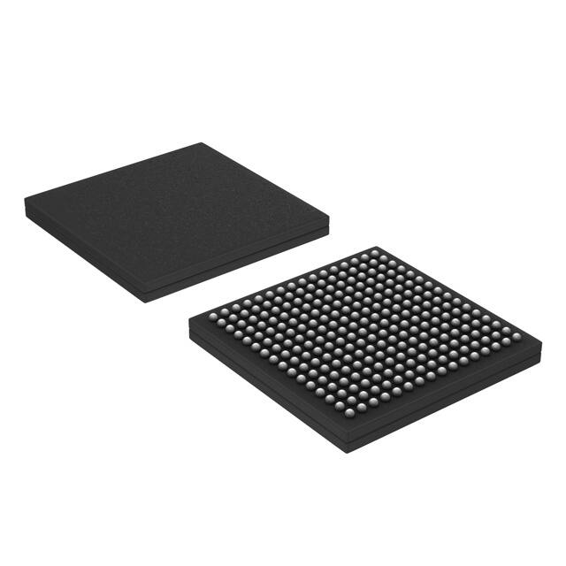


 工商网监
湘ICP备2023018690号
工商网监
湘ICP备2023018690号
