Freescale Semiconductor
Data Sheet: Technical Data
Document Number: MCIMX35SR2AEC
Rev. 10, 06/2012
IMX35
i.MX35 Applications
Processors for
Automotive Products
1
Introduction
The i.MX35 Auto Application Processor family is
designed for automotive infotainment and navigation
applications. These processors are AECQ100 Grade 3
qualified and rated for ambient operating temperatures
up to 85 °C.
Based on an ARM11 microprocessor core running at up
to 532 MHz, the device offers the following features and
optimized system cost for the target applications.
• Audio connectivity and telematics:
— Compressed audio playback from storage
devices (CD, USB, HDD or SD card)
— PlayFromDevice (1-wire and 2-wire
support) for portable media players
— iPod/iPhone control and playback
— High-speed CD ripping to USB, SD/MMC
or HDD for virtual CD changer
— Audio processing for hands-free telephony:
Bluetooth, AEC/NS, and microphone beam
forming
— Speech recognition
© Freescale Semiconductor, Inc., 2010. All rights reserved.
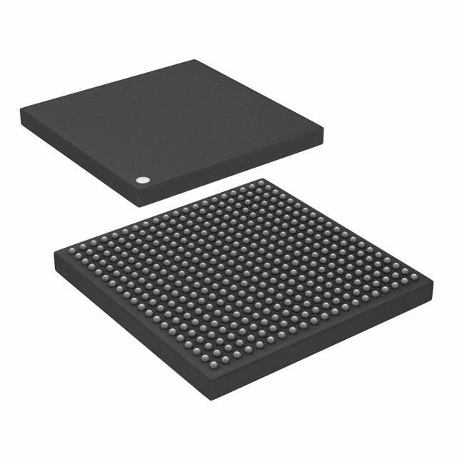
Package Information
Plastic Package
Case 5284 17 x 17 mm, 0.8 mm Pitch
Ordering Information
See Table 1 on page 3 for ordering information.
1. Introduction . . . . . . . . . . . . . . . . . . . . . . . . . . . . . . . . . . . . 1
1.1. Features . . . . . . . . . . . . . . . . . . . . . . . . . . . . . . . . . . 2
1.2 Ordering Information . . . . . . . . . . . . . . . . . . . . . . . . 3
1.3. Block Diagram . . . . . . . . . . . . . . . . . . . . . . . . . . . . . 5
2 Functional Description and Application Information. . . . . . 4
2.1. Application Processor Domain Overview . . . . . . . . . 5
2.2. Shared Domain Overview . . . . . . . . . . . . . . . . . . . . 6
2.3. Advanced Power Management Overview . . . . . . . . 6
2.4. ARM11 Microprocessor Core. . . . . . . . . . . . . . . . . . 6
2.5. Module Inventory . . . . . . . . . . . . . . . . . . . . . . . . . . . 7
3. Signal Descriptions: Special Function Related Pins . . . . 12
4. Electrical Characteristics . . . . . . . . . . . . . . . . . . . . . . . . . 13
4.1. i.MX35 Chip-Level Conditions . . . . . . . . . . . . . . . . 13
4.2. Power Modes . . . . . . . . . . . . . . . . . . . . . . . . . . . . . 15
4.3. Supply Power-Up/Power-Down Requirements and
Restrictions . . . . . . . . . . . . . . . . . . . . . . . . . . . . . . 16
4.4. Reset Timing . . . . . . . . . . . . . . . . . . . . . . . . . . . . . 18
4.5. Power Characteristics . . . . . . . . . . . . . . . . . . . . . . 19
4.6. Thermal Characteristics . . . . . . . . . . . . . . . . . . . . . 20
4.7. I/O Pin DC Electrical Characteristics . . . . . . . . . . . 21
4.8. I/O Pin AC Electrical Characteristics . . . . . . . . . . . 24
4.9. Module-Level AC Electrical Specifications . . . . . . . 30
5. Package Information and Pinout . . . . . . . . . . . . . . . . . . 131
5.1. MAPBGA Production Package 1568-01, 17 × 17 mm,
0.8 Pitch . . . . . . . . . . . . . . . . . . . . . . . . . . . . . . . . 132
5.2. MAPBGA Signal Assignments . . . . . . . . . . . . . . . 133
6. Product Documentation . . . . . . . . . . . . . . . . . . . . . . . . . 145
7. Revision History. . . . . . . . . . . . . . . . . . . . . . . . . . . . . . . 146
�•
A/V connectivity and navigation:
— Includes audio connectivity and telematics features
— Map display and route calculation
— QVGA video decode, WVGA video display
— Sophisticated graphical user interface
The i.MX35 processor takes advantage of the ARM1136JF-S™ core running at 532 MHz that is boosted
by a multilevel cache system, and features peripheral devices such as an autonomous image processing
unit, a vector floating point (VFP11) co-processor, and a RISC-based DMA controller.
The i.MX35 supports connections to various types of external memories, such as SDRAM, mobile DDR
and DDR2, SLC and MLC NAND Flash, NOR Flash and SRAM. The device can be connected to a variety
of external devices such as high-speed USB2.0 OTG, ATA, MMC/SDIO, and Compact Flash.
1.1
Features
The i.MX35 is designed for automotive infotainment video-enabled applications. It provides low-power
solutions for applications demanding high-performance multimedia and graphics.
The i.MX35 is based on the ARM1136 platform, which has the following features:
• ARM1136JF-S processor, version r1p3
• 16-Kbyte L1 instruction cache
• 16-Kbyte L1 data cache
• 128-Kbyte L2 cache, version r0p4
• 128 Kbytes of internal SRAM
• Vector floating point unit (VFP11)
To boost multimedia performance, the following hardware accelerators are integrated:
• Image processing unit (IPU)
• OpenVG 1.1 graphics processing unit (GPU) (not available for the MCIMX351)
The MCIMX35 provides the following interfaces to external devices (some of these interfaces are muxed
and not available simultaneously):
• 2 controller area network (CAN) interfaces
• 2 SDIO/MMC interfaces, 1 SDIO/CE-ATA interface (CE-ATA is not available for the MCIMX351)
• 32-bit mobile DDR, DDR2 (4-bank architecture), and SDRAM (up to 133 MHz)
• 2 configurable serial peripheral interfaces (CSPI) (up to 52 Mbps each)
• Enhanced serial audio interface (ESAI)
• 2 synchronous serial interfaces (SSI)
• Ethernet MAC 10/100 Mbps
• 1 USB 2.0 host with ULPI interface or internal full-speed PHY. Up to 480 Mbps if external HS
PHY is used.
• 1 USB 2.0 OTG (up to 480 Mbps) controller with internal high-speed OTG PHY
i.MX35 Applications Processors for Automotive Products, Rev. 10
2
Freescale Semiconductor
�•
•
•
•
•
•
•
•
•
•
•
•
•
•
1.2
Flash controller—MLC/SLC NAND and NOR
GPIO with interrupt capabilities
3 I2C modules (up to 400 Kbytes each)
JTAG
Key pin port
Media local bus (MLB) interface
Asynchronous sample rate converter (ASRC)
1-Wire
Parallel camera sensor (4/8/10/16-bit data port for video color models: YCC, YUV, 30 Mpixels/s)
Parallel display (primary up to 24-bit, 1024 x 1024)
Parallel ATA (up to 66 Mbytes) (not available for the MCIMX351)
PWM
SPDIF transceiver
3 UART (up to 4.0 Mbps each)
Ordering Information
Table 1 provides the ordering information for the i.MX35 processors for automotive applications.
Table 1. Ordering Information
1
2
Description
Part Number
Silicon
Revision
Package1
Speed
Operating
Temperature
Range (°C)
Signal Ball
Map
Locations
Ball Map
i.MX351
MCIMX351AVM4B
2.0
5284
400 MHz
–40 to 85
Table 94
Table 96
i.MX351
MCIMX351AVM5B
2.0
5284
532 MHz2
–40 to 85
Table 94
Table 96
i.MX355
MCIMX355AVM4B
2.0
5284
400 MHz
–40 to 85
Table 94
Table 96
i.MX355
MCIMX355AVM5B
2.0
5284
532 MHz2
–40 to 85
Table 94
Table 96
i.MX356
MCIMX356AVM4B
2.0
5284
400 MHz
–40 to 85
Table 94
Table 96
i.MX356
MCIMX356AVM5B
2.0
5284
532 MHz2
–40 to 85
Table 94
Table 96
i.MX351
MCIMX351AJQ4C
2.1
5284
400MHz
-40 to 85
Table 95
Table 97
i.MX351
MCIMX351AJQ5C
2.1
5284
532MHz2
-40 to 85
Table 95
Table 97
i.MX355
MCIMX355AJQ4C
2.1
5284
400MHz
-40 to 85
Table 95
Table 97
i.MX355
MCIMX355AJQ5C
2.1
5284
532MHz2
-40 to 85
Table 95
Table 97
i.MX356
MCIMX356AJQ4C
2.1
5284
400MHz
-40 to 85
Table 95
Table 97
i.MX356
MCIMX356AJQ5C
2.1
5284
532MHz2
-40 to 85
Table 95
Table 97
i.MX356
SCIMX356BVMB
2
5284
532MHz
-40 to 85
Table 94
Table 96
Case 5284 is RoHS-compliant, lead-free, MSL = 3, 1.
532 MHz rated devices meet all specifications of 400 MHz rated devices. A 532 MHz device can be substituted in place of a
400 MHz device.
i.MX35 Applications Processors for Automotive Products, Rev. 10
Freescale Semiconductor
3
�The ball map for silicon revision 2.1 is different than the ballmap for silicon revision 2.0. The layout for
each revision is not compatible, so it is important that the correct ballmap be used to implement the layout.
See Section 5, “Package Information and Pinout.”
Table 2 shows the functional differences between the different parts in the i.MX35 family.
Table 2. Functional Differences in the i.MX35 Parts
Module
MCIMX351
MCIMX353
MCIMX355
MCIMX356
MCIMX357
I2C (3)
Yes
Yes
Yes
Yes
Yes
CSPI (2)
Yes
Yes
Yes
Yes
Yes
SSI/I2S (2)
Yes
Yes
Yes
Yes
Yes
ESAI
Yes
Yes
Yes
Yes
Yes
SPDIF I/O
Yes
Yes
Yes
Yes
Yes
USB HS Host
Yes
Yes
Yes
Yes
Yes
USB OTG
Yes
Yes
Yes
Yes
Yes
FlexCAN (2)
Yes
Yes
Yes
Yes
Yes
MLB
Yes
Yes
Yes
Yes
Yes
Ethernet
Yes
Yes
Yes
Yes
Yes
1-Wire
Yes
Yes
Yes
Yes
Yes
KPP
Yes
Yes
Yes
Yes
Yes
SDIO/MMC (2)
Yes
Yes
Yes
Yes
Yes
SDIO/Memory Stick
Yes
Yes
Yes
Yes
Yes
External Memory Controller (EMC)
Yes
Yes
Yes
Yes
Yes
JTAG
Yes
Yes
Yes
Yes
Yes
PATA
—
Yes
Yes
Yes
Yes
CE-ATA
—
Yes
Yes
Yes
Yes
Image Processing Unit (IPU) (inversion
and rotation, pre- and post-processing,
camera interface, blending, display
controller)
—
Yes
Yes
Yes
Yes
Open VG graphics acceleration (GPU)
—
Yes
—
Yes
Yes
i.MX35 Applications Processors for Automotive Products, Rev. 10
4
Freescale Semiconductor
�1.3
Block Diagram
Figure 1 is the i.MX35 simplified interface block diagram.
NOR
Flash/
PSRAM
DDR2/SDDR
RAM
NAND
Flash
Camera
Sensor
External Memory
Interface (EMI)
Smart
DMA
Image
Processing Unit
(IPU)
ARM11
Platform
ARM1136JF-S
SPBA
LCD Display 1 External Graphics
Accelerator
LCD Display 2
VFP
ARM1136 Platform Peripherals
SSI
HS USBOTG
HS USBOTGPHY
AUDMUX
HS USBHost
FS USBPHY
L1 I/D cache
Peripherals
ESAI
MSHC
SPDIF
SSI
ASRC
L2 cache
I2C(3)
AVIC
UART(2)
MAX
CSPI
AIPS (2)
ATA
eSDHC(3)
ETM
UART
CSPI
GPU 2D
Internal
Memory
FEC
CAN(2)
ECT
MLB
IOMUX
IIM
RTICv3
GPIO(3)
RNGC
EPIT
SCC
PWM
Timers
RTC
WDOG
OWIRE
GPT
KPP
3 FuseBox
Audio/Power
Management
JTAG
Bluetooth
MMC/SDIO
or WLAN
Keypad
Connectivity
Access
Figure 1. i.MX35 Simplified Interface Block Diagram
2
Functional Description and Application Information
The i.MX35 consists of the following major subsystems:
• ARM1136 Platform—AP domain
• SDMA Platform and EMI—Shared domain
2.1
Application Processor Domain Overview
The applications processor (AP) and its domain are responsible for running the operating system and
applications software, providing the user interface, and supplying access to integrated and external
peripherals. The AP domain is built around an ARM1136JF-S core with 16-Kbyte instruction and data L1
caches, an MMU, a 128-Kbyte L2 cache, a multiported crossbar switch, and advanced debug and trace
interfaces.
i.MX35 Applications Processors for Automotive Products, Rev. 10
Freescale Semiconductor
5
�The i.MX35 core is intended to operate at a maximum frequency of 532 MHz to support the required
multimedia use cases. Furthermore, an image processing unit (IPU) is integrated into the AP domain to
offload the ARM11 core from performing functions such as color space conversion, image rotation and
scaling, graphics overlay, and pre- and post-processing.
The functionality of AP Domain peripherals includes the user interface; the connectivity, display, security,
and memory interfaces; and 128 Kbytes of multipurpose SRAM.
2.2
Shared Domain Overview
The shared domain is composed of the shared peripherals, a smart DMA engine (SDMA) and a number of
miscellaneous modules. For maximum flexibility, some peripherals are directly accessible by the SDMA
engine.
The i.MX35 has a hierarchical memory architecture including L1 caches and a unified L2 cache. This
reduces the bandwidth demands for the external bus and external memory. The external memory
subsystem supports a flexible external memory system, including support for SDRAM (SDR, DDR2 and
mobile DDR) and NAND Flash.
2.3
Advanced Power Management Overview
To address the continuing need to reduce power consumption, the following techniques are incorporated
in the i.MX35:
• Clock gating
• Power gating
• Power-optimized synthesis
• Well biasing
The insertion of gating into the clock paths allows unused portions of the chip to be disabled. Because
static CMOS logic consumes only leakage power, significant power savings can be realized.
“Well biasing” is applying a voltage that is greater than VDD to the nwells, and one that is lower than VSS
to the pwells. The effect of applying this well back bias voltage reduces the subthreshold channel leakage.
For the 90-nm digital process, it is estimated that the subthreshold leakage is reduced by a factor of ten
over the nominal leakage. Additionally, the supply voltage for internal logic can be reduced from 1.4 V to
1.22 V.
2.4
ARM11 Microprocessor Core
The CPU of the i.MX35 is the ARM1136JF-S core, based on the ARM v6 architecture. This core supports
the ARM Thumb® instruction sets, features Jazelle® technology (which enables direct execution of Java
byte codes) and a range of SIMD DSP instructions that operate on 16-bit or 8-bit data values in 32-bit
registers.
The ARM1136JF-S processor core features are as follows:
• Integer unit with integral EmbeddedICE™ logic
• Eight-stage pipeline
i.MX35 Applications Processors for Automotive Products, Rev. 10
6
Freescale Semiconductor
�•
•
•
•
•
•
•
•
•
•
Branch prediction with return stack
Low-interrupt latency
Instruction and data memory management units (MMUs), managed using micro TLB structures
backed by a unified main TLB
Instruction and data L1 caches, including a non-blocking data cache with hit-under-miss
Virtually indexed/physically addressed L1 caches
64-bit interface to both L1 caches
Write buffer (bypassable)
High-speed Advanced Micro Bus Architecture (AMBA)™ L2 interface
Vector floating point co-processor (VFP) for 3D graphics and hardware acceleration of other
floating-point applications
ETM™ and JTAG-based debug support
Table 3 summarizes information about the i.MX35 core.
Table 3. i.MX35 Core
Core
Acronym
ARM11 or
ARM1136
2.5
Core
Name
ARM1136
Platform
Brief Description
Integrated Memory
Features
The ARM1136™ platform consists of the ARM1136JF-S core, the ETM
real-time debug modules, a 6 × 5 multi-layer AHB crossbar switch (MAX), and
a vector floating processor (VFP).
The i.MX35 provides a high-performance ARM11 microprocessor core and
highly integrated system functions. The ARM Application Processor (AP) and
other subsystems address the needs of the personal, wireless, and portable
product market with integrated peripherals, advanced processor core, and
power management capabilities.
• 16-Kbyte
instruction cache
• 16-Kbyte data
cache
• 128-Kbyte L2
cache
• 32-Kbyte ROM
• 128-Kbyte RAM
Module Inventory
Table 4 shows an alphabetical listing of the modules in the MCIMX35. For extended descriptions of the
modules, see the MCIMX35 reference manual.
Table 4. Digital and Analog Modules
Block
Mnemonic
1-WIRE
ASRC
Block Name
Domain1
Subsystem
Brief Description
1-Wire
interface
ARM
ARM1136
platform
peripherals
1-Wire provides the communication line to a 1-Kbit add-only
memory. the interface can send or receive 1 bit at a time.
Asynchronous
sample rate
converter
SDMA
Connectivity
peripherals
The ASRC is designed to convert the sampling rate of a signal
associated to an input clock into a signal associated to a different
output clock. It supports a concurrent sample rate conversion of
about –120 dB THD+N. The sample rate conversion of each
channel is associated to a pair of incoming and outgoing sampling
rates.
i.MX35 Applications Processors for Automotive Products, Rev. 10
Freescale Semiconductor
7
�Table 4. Digital and Analog Modules (continued)
Block
Mnemonic
Block Name
Domain1
Subsystem
Brief Description
ATA
ATA module
SDMA
Connectivity
peripherals
The ATA block is an AT attachment host interface. Its main use is to
interface with IDE hard disk drives and ATAPI optical disk drives. It
interfaces with the ATA device over a number of ATA signals.
AUDMUX
Digital audio
mux
ARM
Multimedia
peripherals
The AUDMUX is a programmable interconnect for voice, audio, and
synchronous data routing between host serial interfaces (SSIs) and
peripheral serial interfaces (audio codecs). The AUDMUX has two
sets of interfaces: internal ports to on-chip peripherals and external
ports to off-chip audio devices. Data is routed by configuring the
appropriate internal and external ports.
CAN(2)
CAN module
ARM
Connectivity
peripherals
The CAN protocol is primarily designed to be used as a vehicle
serial data bus running at 1 Mbps.
CCM
Clock control
module
ARM
Clocks
This block generates all clocks for the peripherals in the SDMA
platform. The CCM also manages ARM1136 platform low-power
modes (WAIT, STOP), disabling peripheral clocks appropriately for
power conservation, and provides alternate clock sources for the
ARM1136 and SDMA platforms.
CSPI(2)
Configurable
serial
peripheral
interface
SDMA,
ARM
Connectivity
peripherals
This module is a serial interface equipped with data FIFOs; each
master/slave-configurable SPI module is capable of interfacing to
both serial port interface master and slave devices. The CSPI ready
(SPI_RDY) and slave select (SS) control signals enable fast data
communication with fewer software interrupts.
ECT
Embedded
cross trigger
SDMA,
ARM
Debug
ECT (embedded cross trigger) is an IP for real-time debug
purposes. It is a programmable matrix allowing several subsystems
to interact with each other. ECT receives signals required for
debugging purposes (from cores, peripherals, buses, external
inputs, and so on) and propagates them (propagation programmed
through software) to the different debug resources available within
the SoC.
EMI
External
memory
interface
SDMA
External
memory
interface
The EMI module provides access to external memory for the ARM
and other masters. It is composed of the following main
submodules:
M3IF—provides arbitration between multiple masters requesting
access to the external memory.
SDRAM CTRL—interfaces to mDDR, DDR2 (4-bank architecture
type), and SDR interfaces.
NANDFC—provides an interface to NAND Flash memories.
WEIM—interfaces to NOR Flash and PSRAM.
Enhanced
periodic
interrupt timer
ARM
Timer
peripherals
Each EPIT is a 32-bit “set-and-forget” timer that starts counting after
the EPIT is enabled by software. It is capable of providing precise
interrupts at regular intervals with minimal processor intervention. It
has a 12-bit prescaler to adjust the input clock frequency to the
required time setting for the interrupts, and the counter value can be
programmed on the fly.
EPIT(2)
i.MX35 Applications Processors for Automotive Products, Rev. 10
8
Freescale Semiconductor
�Table 4. Digital and Analog Modules (continued)
Block
Mnemonic
ESAI
eSDHCv2
(3)
FEC
GPIO(3)
Block Name
Domain1
Subsystem
Brief Description
Enhanced
serial audio
interface
SDMA
Connectivity
peripherals
The enhanced serial audio interface (ESAI) provides a full-duplex
serial port for serial communication with a variety of serial devices,
including industry-standard codecs, SPDIF transceivers, and other
DSPs. The ESAI consists of independent transmitter and receiver
sections, each section with its own clock generator.
Enhanced
secure digital
host controller
ARM
Connectivity
peripherals
The eSDHCv2 consists of four main modules: CE-ATA, MMC, SD
and SDIO. CE-ATA is a hard drive interface that is optimized for
embedded applications of storage. The MultiMediaCard (MMC) is a
universal, low-cost, data storage and communication media to
applications such as electronic toys, organizers, PDAs, and smart
phones. The secure digital (SD) card is an evolution of MMC and is
specifically designed to meet the security, capacity, performance,
and environment requirements inherent in emerging audio and
video consumer electronic devices. SD cards are categorized into
Memory and I/O. A memory card enables a copyright protection
mechanism that complies with the SDMI security standard. SDIO
cards provide high-speed data I/O (such as wireless LAN via SDIO
interface) with low power consumption.
Note: CE-ATA is not available for the MCIMX351.
Ethernet
SDMA
Connectivity
peripherals
The Ethernet media access controller (MAC) is designed to support
both 10 and 100 Mbps Ethernet/IEEE 802.3 networks. An external
transceiver interface and transceiver function are required to
complete the interface to the media
General
purpose I/O
modules
ARM
Pins
Used for general purpose input/output to external ICs. Each GPIO
module supports 32 bits of I/O.
GPT
General
ARM
purpose timers
Timer
peripherals
Each GPT is a 32-bit free-running or set-and-forget mode timer with
a programmable prescaler and compare and capture registers. A
timer counter value can be captured using an external event and can
be configured to trigger a capture event on either the leading or
trailing edges of an input pulse. When the timer is configured to
operate in set-and-forget mode, it is capable of providing precise
interrupts at regular intervals with minimal processor intervention.
The counter has output compare logic to provide the status and
interrupt at comparison. This timer can be configured to run either
on an external clock or on an internal clock.
GPU2D
Graphics
ARM
processing unit
2Dv1
Multimedia
peripherals
This module accelerates OpenVG and GDI graphics.
Note: Not available for the MCIMX351.
i.MX35 Applications Processors for Automotive Products, Rev. 10
Freescale Semiconductor
9
�Table 4. Digital and Analog Modules (continued)
Block
Mnemonic
Block Name
Domain1
Subsystem
Brief Description
I2C(3)
I2C module
ARM
ARM1136
platform
peripherals
Inter-integrated circuit (I2C) is an industry-standard, bidirectional
serial bus that provides a simple, efficient method of data exchange,
minimizing the interconnection between devices. I2C is suitable for
applications requiring occasional communications over a short
distance among many devices. The interface operates at up to
100 kbps with maximum bus loading and timing. The I2C system is
a true multiple-master bus, with arbitration and collision detection
that prevent data corruption if multiple devices attempt to control the
bus simultaneously. This feature supports complex applications with
multiprocessor control and can be used for rapid testing and
alignment of end products through external connections to an
assembly-line computer.
IIM
IC
identification
module
ARM
Security
modules
The IIM provides the primary user-visible mechanism for interfacing
with on-chip fuse elements. Among the uses for the fuses are
unique chip identifiers, mask revision numbers, cryptographic keys,
and various control signals requiring a fixed value.
IOMUX
External
ARM
signals and pin
multiplexing
Pins
Each I/O multiplexer provides a flexible, scalable multiplexing
solution with the following features:
• Up to eight output sources multiplexed per pin
• Up to four destinations for each input pin
• Unselected input paths held at constant levels for reduced power
consumption
IPUv1
Image
ARM
processing unit
Multimedia
peripherals
The IPU supports video and graphics processing functions. It also
provides the interface for image sensors and displays. The IPU
performs the following main functions:
• Preprocessing of data from the sensor or from the external
system memory
• Postprocessing of data from the external system memory
• Post-filtering of data from the system memory with support of the
MPEG-4 (both deblocking and deringing) and H.264 post-filtering
algorithms
• Displaying video and graphics on a synchronous (dumb or
memory-less) display
• Displaying video and graphics on an asynchronous (smart)
display
• Transferring data between IPU sub-modules and to/from the
system memory with flexible pixel reformatting
KPP
Keypin port
ARM
Connectivity
peripherals
Can be used for either keypin matrix scanning or general purpose
I/O.
MLB
Media local
bus
ARM
Connectivity
peripherals
The MLB is designed to interface to an automotive MOST ring.
OSCAUD
OSC audio
reference
oscillator
Analog
Clock
The OSCAUDIO oscillator provides a stable frequency reference for
the PLLs. This oscillator is designed to work in conjunction with an
external 24.576-MHz crystal.
i.MX35 Applications Processors for Automotive Products, Rev. 10
10
Freescale Semiconductor
�Table 4. Digital and Analog Modules (continued)
Block
Mnemonic
OSC24M
Block Name
Domain1
Subsystem
Brief Description
OSC24M
24-MHz
reference
oscillator
Analog
Clock
The signal from the external 24-MHz crystal is the source of the
CLK24M signal fed into USB PHY as the reference clock and to the
real time clock (RTC).
MPLL
PPLL
Digital
phase-locked
loops
SDMA
Clocks
DPLLs are used to generate the clocks:
MCU PLL (MPLL)—programmable
Peripheral PLL (PPLL)—programmable
PWM
Pulse-width
modulator
ARM
ARM1136
platform
peripherals
The pulse-width modulator (PWM) is optimized to generate sound
from stored sample audio images; it can also generate tones.
RTC
Real-time
clock
ARM
Clocks
Provides the ARM1136 platform with a clock function (days, hours,
minutes, seconds) and includes alarm, sampling timer, and minute
stopwatch capabilities.
Smart DMA
engine
SDMA
System
controls
The SDMA provides DMA capabilities inside the processor. It is a
shared module that implements 32 DMA channels and has an
interface to connect to the ARM1136 platform subsystem, EMI
interface, and the peripherals.
SJC
Secure JTAG
controller
ARM
Pins
The secure JTAG controller (SJC) provides debug and test control
with maximum security.
SPBA
SDMA
peripheral bus
arbiter
SDMA
System
controls
The SPBA controls access to the SDMA peripherals. It supports
shared peripheral ownership and access rights to an owned
peripheral.
S/PDIF
Serial audio
interface
SDMA
Connectivity
peripherals
Sony/Philips digital transceiver interface
SSI(2)
Synchronous
SDMA,
serial interface ARM(2)
Connectivity
peripherals
The SSI is a full-duplex serial port that allows the processor
connected to it to communicate with a variety of serial protocols,
including the Freescale Semiconductor SPI standard and the I2C
sound (I2S) bus standard. The SSIs interface to the AUDMUX for
flexible audio routing.
SDMA
UART(3)
Universal
asynchronous
receiver/trans
mitters
ARM
Connectivity
(UART1,2) peripherals
SDMA
(UART3)
Each UART provides serial communication capability with external
devices through an RS-232 cable using the standard RS-232
non-return-to-zero (NRZ) encoding format. Each module transmits
and receives characters containing either 7 or 8 bits
(program-selectable). Each UART can also provide low-speed IrDA
compatibility through the use of external circuitry that converts
infrared signals to electrical signals (for reception) or transforms
electrical signals to signals that drive an infrared LED (for
transmission).
i.MX35 Applications Processors for Automotive Products, Rev. 10
Freescale Semiconductor
11
�Table 4. Digital and Analog Modules (continued)
Block
Mnemonic
1
Block Name
Domain1
Subsystem
Brief Description
USBOH
High-speed
SDMA
USB on-the-go
Connectivity
peripherals
The USB module provides high performance USB on-the-go (OTG)
functionality (up to 480 Mbps), compliant with the USB 2.0
specification, the OTG supplement, and the ULPI 1.0 low pin count
specification. The module has DMA capabilities handling data
transfer between internal buffers and system memory.
WDOG
Watchdog
modules
Timer
peripherals
Each module protects against system failures by providing a method
of escaping from unexpected events or programming errors. Once
activated, the timer must be serviced by software on a periodic
basis. If servicing does not take place, the watchdog times out and
then either asserts a system reset signal or an interrupt request
signal, depending on the software configuration.
ARM
ARM = ARM1136 platform, SDMA = SDMA platform
3
Signal Descriptions: Special Function Related Pins
Some special functional requirements are supported in the device. The details about these special functions
and the corresponding pin names are listed in Table 5.
Table 5. Special Function Related Pins
Function Name
Pin Name
Mux Mode
EXT_ARMCLK
ALT0
External clock input for ARM clock.
External Peripheral Clock
I2C1_CLK
ALT6
External peripheral clock source.
External 32-kHz Clock
CAPTURE
ALT4
CSPI1_SS1
ALT2
External clock input of 32 kHz, used when the internal
24M Oscillator is powered off, which could be
configured either from CAPTURE or CSPI1_SS1.
CLKO
ALT0
Clock-out pin from CCM, clock source is controllable
and can also be used for debug.
GPIO1_0
ALT1
TX1
ALT1
PMIC power-ready signal, which can be configured
either from GPIO1_0 or TX1.
GPIO1_1
ALT6
External ARM Clock
Clock Out
Power Ready
Tamper Detect
Detailed Description
Tamper-detect logic is used to issue a security
violation. This logic is activated if the tamper-detect
input is asserted. Tamper-detect logic is enabled by the
bit of IOMUXC_GPRA[2]. After enabling the logic, it is
impossible to disable it until the next reset.
i.MX35 Applications Processors for Automotive Products, Rev. 10
12
Freescale Semiconductor
�4
Electrical Characteristics
The following sections provide the device-level and module-level electrical characteristics for the i.MX35
processor.
4.1
i.MX35 Chip-Level Conditions
This section provides the device-level electrical characteristics for the IC. See Table 6 for a quick reference
to the individual tables and sections.
Table 6. i.MX35 Chip-Level Conditions
Characteristics
Table/Location
Absolute Maximum Ratings
Table 7 on page 13
i.MX35 Operating Ranges
Table 8 on page 14
Interface Frequency
Table 9 on page 15
CAUTION
Stresses beyond those listed in Table 7 may cause permanent damage to the
device. These are stress ratings only. Functional operation of the device at
these or any other conditions beyond those indicated in Table 8 is not
implied. Exposure to absolute-maximum-rated conditions for extended
periods may affect device reliability.
Table 7. Absolute Maximum Ratings
Parameter
Symbol
Min.
Max.
Units
Supply voltage (core)
VDDmax1
–0.5
1.47
V
Supply voltage (I/O)
NVCCmax
–0.5
3.6
V
Input voltage range
VImax
–0.5
3.6
V
Tstorage
–40
125
oC
Human Body Model (HBM)
—
20002
Charge Device Model (CDM)
—
5003
Storage temperature
ESD damage immunity:
V
Vesd
1
VDD is also known as QVCC.
HBM ESD classification level according to the AEC-Q100-002 standard
3 Corner pins max. 750 V
2
i.MX35 Applications Processors for Automotive Products, Rev. 10
Freescale Semiconductor
13
�4.1.1
i.MX35 Operating Ranges
Table 8 provides the recommended operating ranges. The term NVCC in this section refers to the
associated supply rail of an input or output.
Table 8. i.MX35 Operating Ranges
Parameter
Symbol
Min.
Typical
Max.
Units
1.22
—
1.47
V
Core Operating Voltage
0 < fARM < 532 MHz
1.33
—
1.47
V
State Retention Voltage
1
—
—
V
VDD
Core Operating Voltage
0 < fARM < 400 MHz
EMI1
NVCC_EMI1,2,3
1.7
—
3.6
V
WTDG, Timer, CCM, CSPI1
NVCC_CRM
1.75
—
3.6
V
NANDF
NVCC_NANDF
1.75
—
3.6
V
ATA, USB generic
NVCC_ATA
1.75
—
3.6
V
eSDHC1
NVCC_SDIO
1.75
—
3.6
V
CSI, SDIO2
NVCC_CSI
1.75
—
3.6
V
JTAG
NVCC_JTAG
1.75
—
3.6
V
LCDC, TTM, I2C1
NVCC_LCDC
1.75
—
3.6
V
I2Sx2,ESAI, I2C2, UART2, UART1, FEC
NVCC_MISC
1.75
—
3.6
V
MLB
NVCC_MLB
2
1.75
—
3.6
V
USB OTG PHY
PHY1_VDDA
3.17
3.3
3.43
V
USB OTG PHY
USBPHY1_VDDA_BIAS
3.17
3.3
3.43
V
USB OTG PHY
USBPHY1_UPLLVDD
3.17
3.3
3.43
V
USB HOST PHY
PHY2_VDD
3.0
3.3
3.6
V
OSC24M
OSC24M_VDD
3.0
3.3
3.6
V
OSC_AUDIO
OSC_AUDIO_VDD
3.0
3.3
3.6
V
MPLL
MVDD
1.4
—
1.65
V
PPLL
PVDD
1.4
—
1.65
V
3.0
3.6
3.6
V
3
Fusebox program supply voltage
FUSE_VDD
Operating ambient temperature range
TA
–40
—
85
oC
Junction temperature range
TJ
–40
—
105
oC
1
EMI I/O interface power supply should be set up according to external memory. For example, if using SDRAM then
NVCC_EMI1,2,3 should all be set at 3.3 V (typ.). If using MDDR or DDR2, NVC_EMI1,2,3 must be set at 1.8 V (typ.).
2 MLB interface I/O pads can be programmed to function as GPIO by setting NVCC_MLB to 1.8 or 3.3 V, but if used as MLB
pads, NVCC_MLB must be set to 2.5 V in order to be compliant with external MOST devices. NVCC_MLB may be left floating.
3
The Fusebox read supply is connected to supply of the full speed USB PHY. FUSE_VDD is only used for programming. It is
recommended that FUSE_VDD be connected to ground when not being used for programming. FUSE_VDD should be
supplied by following the power up sequence given in Section 4.3.1, “Powering Up.”
i.MX35 Applications Processors for Automotive Products, Rev. 10
14
Freescale Semiconductor
�4.1.2
Interface Frequency Limits
Table 9 provides information on interface frequency limits.
Table 9. Interface Frequency
ID
1
4.2
Parameter
Symbol
Min.
Typ.
Max.
Units
fJTAG
DC
5
10
MHz
JTAG TCK Frequency
Power Modes
Table 10 provides descriptions of the power modes of the i.MX35 processor.
Table 10. i.MX35 Power Modes
Power
Mode
Wait
Doze
Description
QVCC (ARM/L2
Peripheral)
MVDD/PVDD
OSC24M_VDD
OSC_AUDO_VDD
Typ.
Max.
Typ.
Max.
Typ.
Max.
VDD1,2,3,4 = 1.1 V (min.)
ARM is in wait for interrupt mode.
MAX is active.
L2 cache is kept powered.
MCU PLL is on (400 MHz)
PER PLL is off (can be configured)
(default: 300 MHz)
Module clocks are gated off (can be
configured by CGR register).
OSC 24M is ON.
OSC audio is off (can be configured).
RNGC internal osc is off.
16 mA
170 mA
7.2 mA
14 mA
1.2 mA
3 mA
VDD1,2,3,4 = 1.1 V (min.)
ARM is in wait for interrupt mode.
MAX is halted.
L2 cache is kept powered.
L2 cache control logic off.
AWB enabled.
MCU PLL is on(400 MHz)
PER PLL is off (can be configured).
(300 Mhz).
Module clocks are gated off (can be
configured by CGR register).
OSC 24M is ON.
OSC audio is off (can be configured)
RNGC internal osc is off
12.4 mA
105 mA
7.2 mA
14 mA
1.2 mA
3 mA
i.MX35 Applications Processors for Automotive Products, Rev. 10
Freescale Semiconductor
15
�Table 10. i.MX35 Power Modes (continued)
Power
Mode
Stop
Static
Description
QVCC (ARM/L2
Peripheral)
MVDD/PVDD
OSC24M_VDD
OSC_AUDO_VDD
Typ.
Max.
Typ.
Max.
Typ.
Max.
VDD1,2,3,4 = 1.1 V (min.)
ARM is in wait for interrupt mode.
MAX is halted
L2 cache is kept powered.
L2 cache control logic off.
AWB enabled.
MCU PLL is off.
PER PLL is off.
All clocks are gated off.
OSC 24 MHz is on
OSC audio is off
RNGC internal osc is off
1.1 mA
77 mA
400 µA
2.2 mA
1.2 mA
2.2 mA
VDD1,2,3,4 = 1.1 V (min.)
ARM is in wait for interrupt mode.
MAX is halted
L2 cache is kept powered.
L2 cache control logic off.
AWB enabled.
MCU PLL is off.
PER PLL is off.
All clocks are gated off.
OSC 24MHz is on
OSC audio is off
RNGC internal osc is off
820 µA
72 mA
50 µA
1.7 mA
24 µA
35 µA
Note: Typical column: TA = 25 °C
Note: Maximum column: TA = 85 °C
4.3
Supply Power-Up/Power-Down Requirements and Restrictions
This section provides power-up and power-down sequence guidelines for the i.MX35 processor.
CAUTION
Any i.MX35 board design must comply with the power-up and power-down
sequence guidelines as described in this section to guarantee reliable
operation of the device. Any deviation from these sequences can result in
irreversible damage to the i.MX35 processor (worst-case scenario).
i.MX35 Applications Processors for Automotive Products, Rev. 10
16
Freescale Semiconductor
�NOTE
Deviation from these sequences may also result in one or more of the
following:
•
•
•
4.3.1
Excessive current during power-up phase
Prevent the device from booting
Programming of unprogrammed fuses
Powering Up
The power-up sequence should be completed as follows:
1. Assert Power on Reset (POR).
2. Turn on digital logic domain and IO power supply: VDDn, NVCCx
3. Wait until VDDn and NVCCx power supplies are stable + 32 μs.
4. Turn on all other power supplies: PHY1_VDDA, USBPHY1_VDDA_BIAS, PHY2_VDD,
USBPHY1_UPLLVDD, OSC24M_VDD, OSC_AUDIO_VDD, MVDD, PVDD, FUSEVDD.
(Always FUSE_VDD should be connected to ground, except when eFuses are to be
programmed.)
5. Wait until PHY1_VDDA, USBPHY1_VDDA_BIAS, PHY2_VDD, USBPHY1_UPLLVDD,
OSC24M_VDD, OSC_AUDIO_VDD, MVDD, PVDD, (FUSEVDD, optional). Power supplies
are stable + 100 μs.
6. Deassert the POR signal.
i.MX35 Applications Processors for Automotive Products, Rev. 10
Freescale Semiconductor
17
�Figure 2 shows the power-up sequence and timing.
Figure 2. i.MX35 Power-Up Sequence and Timing
4.3.2
Powering Down
The power-up sequence in reverse order is recommended for powering down. However, all power supplies
can be shut down at the same time.
4.4
Reset Timing
There are two ways of resetting the i.MX35 using external pins:
• Power On Reset (using the POR_B pin)
• System Reset (using the RESET_IN_B pin)
4.4.1
Power On Reset
POR_B is normally connected to a power management integrated circuit (PMIC). The PMIC asserts
POR_B while the power supplies are turned on and negates POR_B after the power up sequence is
finished. See Figure 2.
i.MX35 Applications Processors for Automotive Products, Rev. 10
18
Freescale Semiconductor
�Assuming the i.MX35 chip is already fully powered; it is still possible to reset all of the modules to their
default reset by asserting POR_B for at least 4 CKIL cycles and later de-asserting POR_B. This method
of resetting the i.MX35 can also be supported by tying the POR_B and RESET_IN_B pins together.
POR_B
At least 4 CKIL cycles
CKIL
Figure 3. Timing Between POR_B and CKIL for Complete Reset of i.MX35
4.4.2
System Reset
System reset can be achieved by asserting RESET_IN_B for at least 4 CKIL cycles and later negating
RESET_IN_B. The following modules are not reset upon system reset: RTC, PLLs, CCM, and IIM.
POR_B pin must be deasserted all the time.
RESET_IN_B
At least 4 CKIL cycles
CKIL
Figure 4. Timing Between RESET_IN_B and CKIL for i.MX35 System Reboot
4.5
Power Characteristics
The table shows values representing maximum current numbers for the i.MX35 under worst case voltage
and temperature conditions. These values are derived from the i.MX35 with core clock speeds up to
532 MHz. Common supplies have been bundled according to the i.MX35 power-up sequence
requirements. Peak numbers are provided for system designers so that the i.MX35 power supply
requirements will be satisfied during startup and transient conditions. Freescale recommends that system
current measurements be taken with customer-specific use-cases to reflect normal operating conditions in
the end system.
i.MX35 Applications Processors for Automotive Products, Rev. 10
Freescale Semiconductor
19
�Table 11. Power Consumption
Power Supply
Voltage (V)
Max Current (mA)
QVCC
1.47
400
MVDD, PVDD
1.65
20
NVCC_EMI1, NVCC_EMI2, NVCC_EMI3, NVCC_LCDC, NVCC_NFC
1.9
90
FUSE_VDD1
3.6
62
NVCC_MISC, NVCC_CSI, NVCC_SDIO, NVCC_CRM, NVCC_ATA, NVCC_MLB,
NVCC_JTAG
3.6
60
OSC24M_VDD, OSC_AUDIO_VDD, PHY1_VDDA, PHY2_VDD,
USBPHY1_UPLLVDD, USBPHY1_VDDA_BIAS
3.6
25
1
This rail is connected to ground; it only needs a voltage if eFuses are to be programmed. FUSE_VDD should be supplied by
following the power up sequence given in Section 4.3.1, “Powering Up.”
The method for obtaining max current is as follows:
1. Measure worst case power consumption on individual rails using directed test on i.MX35.
2. Correlate worst case power consumption power measurements with worst case power
consumption simulations.
3. Combine common voltage rails based on power supply sequencing requirements
4. Guard band worst case numbers for temperature and process variation. Guard band is based on
process data and correlated with actual data measured on i.MX35.
5. The sum of individual rails is greater than real world power consumption, as a real system does
not typically maximize power consumption on all peripherals simultaneously.
4.6
Thermal Characteristics
The thermal resistance characteristics for the device are given in Table 12. These values were measured
under the following conditions:
• Two-layer substrate
• Substrate solder mask thickness: 0.025 mm
• Substrate metal thicknesses: 0.016 mm
• Substrate core thickness: 0.200 mm
• Core via I.D: 0.168 mm, Core via plating 0.016 mm.
• Full array map design, but nearly all balls under die are power or ground.
• Die Attach: 0.033 mm non-conductive die attach, k = 0.3 W/m K
• Mold compound: k = 0.9 W/m K
Table 12. Thermal Resistance Data
Rating
Condition
Symbol
Value
Unit
Junction to ambient1 natural convection
Single layer board (1s)
ReJA
53
ºC/W
1
Four layer board (2s2p)
ReJA
30
ºC/W
Junction to ambient natural convection
i.MX35 Applications Processors for Automotive Products, Rev. 10
20
Freescale Semiconductor
�Table 12. Thermal Resistance Data (continued)
Rating
Condition
Symbol
Value
Unit
Junction to ambient1 (at 200 ft/min)
Single layer board (1s)
ReJMA
44
ºC/W
Junction to ambient1 (at 200 ft/min)
Four layer board (2s2p)
ReJMA
27
ºC/W
—
ReJB
19
ºC/W
—
ReJCtop
10
ºC/W
Natural convection
ΨJT
2
ºC/W
Junction to boards
2
Junction to case (top)3
Junction to package top4
1
Junction-to-ambient thermal resistance determined per JEDC JESD51-3 and JESD51-6. Thermal test board meets JEDEC
specification for this package.
2
Junction-to-board thermal resistance determined per JEDC JESD51-8. Thermal test board meets JEDEC specification for this
package.
3
Junction-to-case at the top of the package determined using MIL-STD 883 Method 1012.1. The cold plate temperature is used
for the case temperature. Reported value includes the thermal resistance of the interface layer.
4 Thermal characterization parameter indicating the temperature difference between the package top and the junction
temperature per JEDEC JESD51-2. When Greek letters are not available, this thermal characterization parameter is written
as Psi-JT.
4.7
I/O Pin DC Electrical Characteristics
I/O pins are of two types: GPIO and DDR. DDR pins can be configured in three different drive strength
modes: mobile DDR, SDRAM, and DDR2. The SDRAM and mobile DDR modes can be further
customized at three drive strength levels: normal, high, and max.
Table 13 shows currents for the different DDR pin drive strength modes.
Table 13. DDR Pin Drive Strength Mode Current Levels
Drive Mode
Normal
High
Max.
3.6 mA
7.2 mA
10.8 mA
SDRAM (1.8 V)
—
—
6.5 mA
SDRAM (3.3 V)
4 mA
8 mA
12 mA
—
—
13.4 mA
Mobile DDR (1.8 V)
DDR2 (1.8 V)
i.MX35 Applications Processors for Automotive Products, Rev. 10
Freescale Semiconductor
21
�Table 14 shows the DC electrical characteristics for GPIO, DDR2, mobile DDR, and SDRAM pins. The
term NVCC refers to the power supply voltage that feeds the I/O of the module in question. For example,
NVCC for the SD/MMC interface refers to NVCC_SDIO.
Table 14. I/O Pin DC Electrical Characteristics
Pin
GPIO
DC Electrical Characteristics Symbol
Test Condition
Min.
Typ.
Max.
Unit
High-level output voltage
Voh
Ioh = –1 mA
Ioh = specified drive
NVCC – 0.15
0.8 × NVCC
—
—
V
Low-level output voltage
Vol
Iol = 1 mA
Iol = specified drive
—
—
0.15
0.2 × NVCC
V
High-level output current for
slow mode
(Voh = 0.8 × NVCC)
Ioh
Standard drive
High drive
Max. drive
–2.0
–4.0
–8.0
—
—
mA
High-level output current
for fast mode
(Voh = 0.8 × NVCC)
Ioh
Standard drive
High drive
Max. drive
–4.0
–6.0
–8.0
—
—
mA
Low-level output current
for slow mode
(Voh = 0.2 × NVCC)
Iol
Standard drive
High drive
Max. drive
2.0
4.0
8.0
—
—
mA
Low-level output current
for fast mode
(Voh = 0.2 × NVCC)
Iol
Standard drive
High drive
Max. drive
4.0
6.0
8.0
—
—
mA
High-level DC Input
Voltage with 1.8 V,
3.3 V NVCC (for digital
cells in input mode)
VIH
—
0.7 × NVCC
—
NVCC
V
Low-level DC Input
Voltage with 1.8 V,
3.3 V NVCC (for digital
cells in input mode
VIL
—
–0.3 V
—
0.3 × NVCC
V
VHYS
OVDD = 3.3 V
OVDD = 1.8 V
—
410
330
—
mV
Schmitt trigger VT+
VT+
—
0.5 × NVCC
—
Schmitt trigger VT–
VT–
—
—
—
0.5 × NVCC
V
Pull-up resistor
(22 kΩ PU)
Rpu
Vi = 0
—
22
—
kΩ
Pull-up resistor
(47 kΩ PU)
Rpu
Vi = 0
—
47
—
kΩ
Pull-up resistor
(100 kΩ PU)
Rpu
Vi = 0
—
100
—
kΩ
Pull-down resistor (100 kΩ PD)
Rpd
Vi = NVCC
—
100
—
kΩ
External resistance to pull
keeper up when enabled
Rkpu
Ipu > 620 μA
@ min Vddio = 3.0 V
—
—
4.8
kΩ
External resistance to pull
keeper down when enabled
Rkpd
Ipu > 510 μA
@min Vddio = 3.0 V
—
—
5.9
kΩ
Input Hysteresis
V
i.MX35 Applications Processors for Automotive Products, Rev. 10
22
Freescale Semiconductor
�Table 14. I/O Pin DC Electrical Characteristics (continued)
Pin
DDR2
DC Electrical Characteristics Symbol
Min.
Typ.
Max.
Unit
NVCC – 0.28
—
—
V
—
0.28
V
High-level output voltage
Voh
—
Low-level output voltage
Vol
—
Output min. source current
Ioh
—
–13.4
—
—
mA
Output min. sink current
Iol
—
13.4
—
—
mA
DC input logic high
VIH(dc)
—
NVCC ÷ 2 +
0.125
—
NVCC + 0.3
V
DC input logic low
VIL(dc)
—
–0.3 V
—
NVCC ÷ 2 –
0.125
V
DC input signal voltage
(for differential signal)
Vin(dc)
—
–0.3
—
NVCC + 0.3
V
DC differential input voltage
Vid(dc)
—
0.25
—
NVCC + 0.6
V
Termination voltage
Vtt
—
NVCC ÷ 2 –
0.04
NV
CC
÷2
NVCC ÷ 2 +
0.04
V
Input current (no
pull-up/down)
IIN
—
—
—
±1
μA
Icc – N
VCC
—
—
—
±1
μA
High-level output voltage
—
IOH = –1mA
IOH = specified drive
NVCC – 0.08
0.8 × NVCC
—
—
V
Low-level output voltage
—
IOL = 1mA
IOL = specified drive
—
—
0.08
0.2 × NVCC
V
High-level output current
(Voh = 0.8 × NVCCV)
—
Standard drive
High drive
Max. drive
–3.6
–7.2
–10.8
—
—
mA
Low-level output current
(Vol = 0.2 × NVCCV)
—
Standard Drive
High Drive
Max. Drive
3.6
7.2
10.8
—
—
mA
High-Level DC CMOS
input voltage
VIH
—
0.7 × NVCC
—
NVCC + 0.3
V
Low-Level DC CMOS
input voltage
VIL
—
–0.3
—
0.2 × NVCC
V
Differential receiver VTH+
VTH+
—
—
—
100
mV
Differential receiver VTH–
VTH–
—
–100
—
IIN
VI = 0
VI = NVCC
—
—
±1
μA
Icc – N
VCC
VI = NVCC or 0
—
—
±1
μA
Tri-state I/O supply current
Mobile
DDR
Test Condition
Input current (no
pull-up/down)
Tri-state I/O supply current
mV
i.MX35 Applications Processors for Automotive Products, Rev. 10
Freescale Semiconductor
23
�Table 14. I/O Pin DC Electrical Characteristics (continued)
Pin
DC Electrical Characteristics Symbol
Test Condition
Min.
Typ.
Max.
Unit
SDR High-level output voltage
(1.8 V)
Low-level output voltage
Voh
loh = 5.7 mA
OVDD – 0.28
—
—
V
Vol
loh = 5.7 mA
—
—
0.4
V
High-level output current
Ioh
Max. drive
5.7
—
—
mA
Low-level output current
Iol
Max. drive
7.3
—
—
mA
High-level DC Input Voltage
VIH
—
1.4
—
1.98
V
Low-level DC Input Voltage
VIL
—
–0.3
—
0.8
V
Input current (no
pull-up/down)
IIN
VI = 0
VI=NVCC
—
—
150
80
μA
Tri-state I/O supply current
Icc
(NVCC)
VI = OVDD or 0
—
—
1180
μA
Tri-state core supply current
Icc
(NVCC)
VI = VDD or 0
—
—
1220
μA
SDR High-level output voltage
(3.3 V)
Voh
Ioh=specified drive
(Ioh = –4, –8, –12,
–16 mA)
2.4
—
—
V
Low-level output voltage
Vol
Ioh=specified drive (Ioh = 4,
8, 12, 16 mA)
—
—
0.4
V
High-level output current
Ioh
Standard drive
High drive
Max. drive
–4.0
–8.0
–12.0
—
—
mA
Low-level output current
Iol
Standard drive
High drive
Max. drive
4.0
8.0
12.0
—
—
mA
High-level DC Input Voltage
VIH
—
2.0
—
3.6
V
Low-level DC Input Voltage
VIL
—
–0.3V
—
0.8
V
Input current (no
pull-up/down)
IIN
VI = 0
—
—
±1
μA
—
—
±1
μA
VI = NVCC
Tri-state I/O supply current
4.8
Icc
(NVCC)
VI = NVCC or 0
I/O Pin AC Electrical Characteristics
Figure 5 shows the load circuit for output pins.
From Output
Under Test
Test Point
CL
CL includes package, probe and jig capacitance
Figure 5. Load Circuit for Output Pin
i.MX35 Applications Processors for Automotive Products, Rev. 10
24
Freescale Semiconductor
�Figure 6 shows the output pin transition time waveform.
NVCC
80%
80%
20%
0V
20%
Output (at pin)
PA1
PA1
Figure 6. Output Pin Transition Time Waveform
4.8.1
AC Electrical Test Parameter Definitions
AC electrical characteristics in Table 16 through Table 21 are not applicable for the output open drain
pull-down driver.
The dI/dt parameters are measured with the following methodology:
• The zero voltage source is connected between pin and load capacitance.
• The current (through this source) derivative is calculated during output transitions.
Table 15. AC Requirements of I/O Pins
Parameter
Symbol
Min.
Max.
Units
AC input logic high
VIH(ac)
NVCC ÷ 2 + 0.25
NVCC + 0.3
V
AC input logic low
VIL(ac)
–0.3
NVCC ÷ 2 – 0.25
V
Table 16. AC Electrical Characteristics of GPIO Pins in Slow Slew Rate Mode
[NVCC = 3.0 V–3.6 V]
Symbol
Test
Condition
Min.
Rise/Fall
Typ. Rise/Fall
Max.
Rise/Fall
Units
Fduty
—
40
—
60
%
Output pin slew rate (max. drive)
tps
25 pF
50 pF
0.79/1.12
0.49/0.73
1.30/1.77
0.84/1.23
2.02/2.58
1.19/1.58
V/ns
Output pin slew rate (high drive)
tps
25 pF
50 pF
0.48/0.72
0.27/0.42
0.76/1.10
0.41/0.62
1.17/1.56
0.63/0.86
V/ns
Output pin slew rate (standard
drive)
tps
25 pF
50 pF
0.25/0.40
0.14/0.21
0.40/0.59
0.21/0.32
0.60/0.83
0.32/0.44
V/ns
Output pin di/dt (max. drive)
tdit
25 pF
50 pF
15
16
36
38
76
80
mA/ns
Output pin di/dt (high drive)
tdit
25 pF
50 pF
8
9
20
21
45
47
mA/ns
Output pin di/dt (standard
drive)
tdit
25 pF
50 pF
4
4
10
10
22
23
mA/ns
Parameter
Duty cycle
i.MX35 Applications Processors for Automotive Products, Rev. 10
Freescale Semiconductor
25
�Table 17. AC Electrical Characteristics of GPIO Pins in Slow Slew Rate Mode
[NVCC = 1.65 V–1.95 V]
Symbol
Test Condition
Min.
Rise/Fall
Typ.
Max.
Rise/Fall
Units
Fduty
—
40
—
60
%
Output pin slew rate (max. drive)
tps
25 pF
50 pF
0.30/0.42
0.20/0.29
0.54/0.73
0.35/0.50
0.91/1.20
0.60/0.80
V/ns
Output pin slew rate (high drive)
tps
25 pF
50 pF
0.19/0.28
0.12/0.18
0.34/0.49
0.34/0.49
0.58/0/79
0.36/0.49
V/ns
Output pin slew rate (standard drive)
tps
25 pF
50 pF
0.12/0.18
0.07/0.11
0.20/0.30
0.11/0.17
0.34/0.47
0.20/0.27
V/ns
Output pin di/dt (max. drive)
tdit
25 pF
50 pF
7
7
21
22
56
58
mA/ns
Output pin di/dt (high drive)
tdit
25 pF
50 pF
5
5
14
15
38
40
mA/ns
Output pin di/dt (standard
drive)
tdit
25 pF
50 pF
2
2
7
7
18
19
mA/ns
Parameter
Duty cycle
Table 18. AC Electrical Characteristics of GPIO Pins in Fast Slew Rate Mode for
[NVCC = 3.0 V–3.6 V]
Symbol
Test Condition
Min.
rise/fall
Typ.
Max.
Rise/Fall
Units
Fduty
—
40
—
60
%
Output pin slew rate (max. drive)
tps
25 pF
50 pF
0.96/1.40
0.54/0.83
1.54/2.10
0.85/1.24
2.30/3.00
1.26/1.70
V/ns
Output pin slew rate (high drive)
tps
25 pF
50 pF
0.76/1.10
0.41/0.64
1.19/1.71
0.63/0.95
1.78/2.39
0.95/1.30
V/ns
Output pin slew rate (standard drive)
tps
25 pF
50 pF
0.52/0.78
0.28/0.44
0.80/1.19
0.43/0.64
1.20/1.60
0.63/0.87
V/ns
Output pin di/dt (max. drive)
tdit
25 pF
50 pF
46
49
108
113
250
262
mA/ns
Output pin di/dt (high drive)
tdit
25 pF
50 pF
35
37
82
86
197
207
mA/ns
Output pin di/dt (standard
drive)
tdit
25 pF
50 pF
22
23
52
55
116
121
mA/ns
Parameter
Duty cycle
i.MX35 Applications Processors for Automotive Products, Rev. 10
26
Freescale Semiconductor
�Table 19. AC Electrical Characteristics, GPIO Pins in Fast Slew Rate Mode
[NVCC = 1.65 V–1.95 V]
Symbol
Test Condition
Min.
Rise/Fall
Typ.
Max.
Rise/Fall
Units
Fduty
—
40
—
60
%
Output pin slew rate (max. drive)
tps
25 pF
50 pF
0.40/0.57
0.25/0.36
0.72/0.97
0.43/0.61
1.2/1.5
0.72/0.95
V/ns
Output pin slew rate (high drive)
tps
25 pF
50 pF
0.38/0.48
0.20/0.30
0.59/0.81
0.34/0.50
0.98/1.27
0.56/0.72
V/ns
Output pin slew rate (standard drive)
tps
25 pF
50 pF
0.23/0.32
0.13/0.20
0.40/0.55
0.23/0.34
0.66/0.87
0.38/0.52
V/ns
Output pin di/dt (max. drive)
tdit
25 pF
50 pF
7
7
43
46
112
118
mA/ns
Output pin di/dt (high drive)
tdit
25 pF
50 pF
11
12
31
33
81
85
mA/ns
Output pin di/dt (standard
drive)
tdit
25 pF
50 pF
9
10
27
28
71
74
mA/ns
Parameter
Duty cycle
Table 20. AC Electrical Characteristics of GPIO Pins in Slow Slew Rate Mode
[NVCC = 2.25 V–2.75 V]
Symbol
Test Condition
Min.
Rise/Fall
Typ.
Max.
Rise/Fall
Units
Fduty
—
40
—
60
%
Output pin slew rate (max. drive)
tps
25 pF
40 pF
50 pF
0.63/0.85
0.52/0.67
0.41/0.59
1.10/1.40
0.90/1.10
0.73/0.99
1.86/2.20
1.53/1.73
1.20/1.50
V/ns
Output pin slew rate (high drive)
tps
25 pF
40 pF
50 pF
0.40/0.58
0.33/0.43
0.25/0.37
0.71/0.98
0.56/0.70
0.43/0.60
1.16/1.40
0.93/1.07
0.68/0.90
V/ns
Output pin slew rate (standard drive)
tps
25 pF
40 pF
50 pF
0.24/0.36
0.19/0.25
0.13/0.21
0.41/0.59
0.32/0.35
0.23/0.33
0.66/0.87
0.51/0.59
0.36/0.48
V/ns
Output pin di/dt (max. drive)
tdit
25 pF
50 pF
22
23
62
65
148
151
mA/ns
Output pin di/dt (high drive)
tdit
25 pF
50 pF
15
16
42
44
102
107
mA/ns
Output pin di/dt (standard
drive)
tdit
25 pF
50 pF
7
8
21
22
52
54
mA/ns
Parameter
Duty cycle
i.MX35 Applications Processors for Automotive Products, Rev. 10
Freescale Semiconductor
27
�Table 21. AC Electrical Characteristics of GPIO Pins in Fast Slew Rate Mode
[NVCC = 2.25 V–2.75 V]
Parameter
Symbol
Duty cycle
Test
Min.
Condition Rise/Fall
Fduty
—
Output pin slew rate (max. drive)
tps
25 pF
40 pF
50 pF
Output pin slew rate (high drive)
tps
Output pin slew rate (standard drive)
Max.
Units Notes
Rise/Fall
Typ.
%
—
0.84/1.10 1.45/1.80 2.40/2.80
0.68/0.83 1.14/1.34 1.88/2.06
0.58/0.72 0.86/1.10 1.40/1.70
V/ns
2
25 pF
40 pF
50 pF
0.69/0.96 1.18/1.50 1.90/2.30
0.55/0.69 0.92/1.10 1.49/1.67
0.40/0.59 0.67/0.95 1.10/1.30
V/ns
tps
25 pF
40 pF
50 pF
0.24/0.36 0.80/1.00 1.30/1.60
0.37/0.47 0.62/0.76 1.00/1.14
0.13/0.21 0.45/0.65 0.70/0.95
V/ns
Output pin di/dt (max. drive)
tdit
25 pF
50 pF
46
49
124
131
310
324
mA/ns
Output pin di/dt (high drive)
tdit
25 pF
50 pF
33
35
89
94
290
304
mA/ns
Output pin di/dt (standard
drive)
tdit
25 pF
50 pF
28
29
75
79
188
198
mA/ns
4.8.2
40
—
60
3
AC Electrical Characteristics for DDR Pins (DDR2, Mobile DDR, and
SDRAM Modes)
Table 22. AC Electrical Characteristics of DDR Type IO Pins in DDR2 Mode
Symbol
Test Condition
Min.
Rise/Fall
Typ.
Max.
Rise/Fall
Units
Fduty
—
45
50
55
%
f
—
—
133
—
MHz
Output pin slew rate
tps
25 pF
50 pF
0.86/0.98
0.46/054
1.35/1.5
0.72/0.81
2.15/2.19
1.12/1.16
V/ns
Output pin di/dt
tdit
25 pF
50 pF
65
70
157
167
373
396
mA/ns
Parameter
Duty cycle
Clock frequency
Table 23. AC Requirements of DDR2 Pins
Parameter1
Symbol
Min.
Max.
AC input logic high
VIH(ac)
NVCC ÷ 2 + 0.25
NVCC + 0.3
V
AC input logic low
VIL(ac)
–0.3
NVCC ÷ 2 – 0.25
V
AC differential cross point voltage for output2
Vox(ac)
NVCC ÷ 2 – 0.125
NVCC ÷ 2 + 0.125
V
1
Units
The Jedec SSTL_18 specification (JESD8-15a) for an SSTL interface for class II operation supersedes any specification in this
document.
i.MX35 Applications Processors for Automotive Products, Rev. 10
28
Freescale Semiconductor
�2
The typical value of Vox(ac) is expected to be about 0.5 × NVCC and Vox(ac) is expected to track variation in NVCC. Vox(ac)
indicates the voltage at which the differential output signal must cross. Cload = 25 pF.
Table 24. AC Electrical Characteristics of DDR Type IO Pins in mDDR Mode
Symbol
Test Condition
Min.
Rise/Fall
Typ.
Max.
Rise/Fall
Units
Fduty
—
45
50
55
%
f
—
—
133
—
MHz
Output pin slew rate (max. drive)
tps
25 pF
50 pF
0.80/0.92
0.43/0.50
1.35/1.50
0.72/0.81
2.23/2.27
1.66/1.68
V/ns
Output pin slew rate (high drive)
tps
25 pF
50 pF
0.37/0.43
0.19/0.23
0.62/0.70
0.33/0.37
1.03/1.05
0.75/0.77
V/ns
Output pin slew rate (standard drive)
tps
25 pF
50 pF
0.18/0.22
0.10/0.12
0.31/0.35
0.16/0.18
0.51/0.53
0.38/0.39
V/ns
Output pin di/dt (max. drive)
tdit
25 pF
50 pF
64
69
171
183
407
432
mA/ns
Output pin di/dt (high drive)
tdit
25 pF
50 pF
37
39
100
106
232
246
mA/ns
Output pin di/dt (standard drive)
tdit
25 pF
50 pF
18
20
50
52
116
123
mA/ns
Parameter
Duty cycle
Clock frequency
Table 25. AC Electrical Characteristics of DDR Type IO Pins in SDRAM Mode
Symbol
Test Condition
Min.
Rise/Fall
Min. Clock
Frequency
Max.
Rise/Fall
Units
f
—
—
125
—
MHz
Output pin slew rate (max. drive)
tps
25 pF
50 pF
1.11/1.20
0.97/0.65
1.74/1.75
0.92/0.94
2.42/2.46
1.39/1.30
V/ns
Output pin slew rate (high drive)
tps
25 pF
50 pF
0.76/0.80
0.40/0.43
1.16/1.19
0.61/0.63
1.76/1.66
0.93/0.87
V/ns
Output pin slew rate (standard drive)
tps
25 pF
50 pF
0.38/0.41
0.20/0.22
0.59/0.60
0.31/0.32
0.89/0.82
0.47/0.43
V/ns
Output pin di/dt (max. drive)
tdit
25 pF
50 pF
89
94
198
209
398
421
mA/ns
Output pin di/dt (high drive)
tdit
25 pF
50 pF
59
62
132
139
265
279
mA/ns
Output pin di/dt (standard drive)
tdit
25 pF
50 pF
29
31
65
69
132
139
mA/ns
Parameter
Clock frequency
i.MX35 Applications Processors for Automotive Products, Rev. 10
Freescale Semiconductor
29
�Table 26. AC Electrical Characteristics of DDR Type IO Pins in SDRAM Mode Max Drive (1.8 V)
Symbol
Test Condition
Min.
Rise/Fall
Typ.
Max.
Rise/Fall
Units
f
—
125
—
—
MHz
tps
25 pF
50 pF
2.83/2.68
1.59/1.49
1.84/1.85
1.03/1.05
1.21/1.40
0.70/0.75
V/ns
Output pin di/dt (max. drive)2
didt
25 pF
50 pF
89
95
202
213
435
456
mA/ns
Input pin transition times3
trfi
1.0 pF
0.07/0.08
0.11/0.12
0.16/0.20
ns
Input pin propagation delay, 50%–50%
tpi
1.0 pF
0.35/1.17
0.63/1.53
1.16/2.04
ns
Input pin propagation delay, 40%–60%
tpi
1.0 pF
1.18/1.99
1.45/2.35
1.97/2.85
ns
Parameter
Clock frequency
Output pin slew rate (max. drive)
1
1
Min. condition for tps: wcs model, 1.1 V, IO 1.65 V, and 105 °C. tps is measured between VIL to VIH for rising edge and between
VIH to VIL for falling edge.
2 Max. condition for tdit: bcs model, 1.3 V, IO 1.95 V, and –40 °C.
3 Max. condition for tpi and trfi: wcs model, 1.1 V, IO 1.65 V and 105 °C. Min. condition for tpi and trfi: bcs model, 1.3 V, IO 1.95 V
and –40 °C. Input transition time from pad is 5 ns (20%–80%).
4.9
Module-Level AC Electrical Specifications
This section contains the AC electrical information (including timing specifications) for the modules of
the i.MX35. The modules are listed in alphabetical order.
4.9.1
AUDMUX Electrical Specifications
The AUDMUX provides a programmable interconnect logic for voice, audio and data routing between
internal serial interfaces (SSI) and external serial interfaces (audio and voice codecs). The AC timing of
AUDMUX external pins is hence governed by the SSI module. See the electrical specification for SSI.
4.9.2
CSPI AC Electrical Specifications
The i.MX35 provides two CSPI modules. CSPI ports are multiplexed in the i.MX35 with other pins. See
the “External Signals and Multiplexing” chapter of the reference manual for more details.
i.MX35 Applications Processors for Automotive Products, Rev. 10
30
Freescale Semiconductor
�Figure 7 and Figure 8 depict the master mode and slave mode timings of the CSPI, and Table 27 lists the
timing parameters.
SPI_RDY
CS11
SSn[3:0]
CS1
CS3
CS2
CS6
CS5
CS3
CS4
SCLK
CS2
CS7 CS8
MOSI
CS9
CS10
MISO
Figure 7. CSPI Master Mode Timing Diagram
SSn[3:0]
CS1
CS3
CS2
CS5
CS6
CS4
SCLK
CS9
CS3
CS10
CS2
MISO
CS8
CS7
MOSI
Figure 8. CSPI Slave Mode Timing Diagram
Table 27. CSPI Interface Timing Parameters
ID
Parameter
Symbol
Min.
Max.
Units
CS1
SCLK cycle time
tclk
60
—
ns
CS2
SCLK high or low time
tSW
30
—
ns
CS3
SCLK rise or fall
tRISE/FALL
—
7.6
ns
CS4
SSn[3:0] pulse width
tCSLH
30
—
ns
CS5
SSn[3:0] lead time (CS setup time)
tSCS
30
—
ns
CS6
SSn[3:0] lag time (CS hold time)
tHCS
30
—
ns
CS7
MOSI setup time
tSmosi
5
—
ns
CS8
MOSI hold time
tHmosi
5
—
ns
CS9
MISO setup time
tSmiso
5
—
ns
i.MX35 Applications Processors for Automotive Products, Rev. 10
Freescale Semiconductor
31
�Table 27. CSPI Interface Timing Parameters (continued)
ID
Parameter
Symbol
Min.
Max.
Units
CS10
MISO hold time
tHmiso
5
—
ns
CS11
SPI_RDY setup time
tSDRY
5
—
ns
4.9.3
DPLL Electrical Specifications
There are three PLLs inside the i.MX35, all based on the same PLL design. The reference clock for these
PLLs is normally generated from an external 24-MHz crystal connected to an internal oscillator via
EXTAL24M and XTAL24 pins. It is also possible to connect an external 24-MHz clock directly to
EXTAL24M, bypassing the internal oscillator.
DPLL specifications are listed in Table 28.
Table 28. DPLL Specifications
Parameter
Min. Typ. Max.
Unit
Comments
Reference clock frequency
10
24
100
Max. allowed reference clock phase noise
—
—
0.03 2 Tdck1 Fmodulation < 50 kHz
0.01
50 kHz < Fmodulation 300 Hz
0.15
Fmodulation > 300 KHz
Frequency lock time (FOL mode or non-integer MF)
—
—
80
μs
—
Phase lock time
—
—
100
μs
—
Max. allowed PL voltage ripple
—
—
150
100
150
mV
1
MHz
Fmodulation < 50 kHz
50 kHz < Fmodulation 300 Hz
Fmodulation > 300 KHz
There are two PLL are used in the i.MX35, MPLL and PPLL. Both are based on same DPLL design.
If crystals are used instead of external oscillators, they should meed the following specifications:
Table 29. Clock Input Tolerance
Parameters
OSC24M
OSC_AUDIO
Normal Frequency
24 MHz
25.576 MHz
Frequency Tolerance
30 ppm
20 ppm (high quality)
ESR