NXP Semiconductors
Document Number: IMX6ULAEC
Rev. 2.2, 05/2017
Data Sheet: Technical Data
MCIMX6G1AVM05AA
MCIMX6G1AVM07AA
MCIMX6G2AVM05AA
MCIMX6G2AVM07AA
MCIMX6G1AVM05AB
MCIMX6G1AVM07AB
MCIMX6G2AVM05AB
MCIMX6G2AVM07AB
i.MX 6UltraLite
Automotive Applications
Processors
Package Information
Plastic Package
BGA 14 x 14 mm, 0.8 mm pitch
Ordering Information
See Table 1 on page 3
1
i.MX 6UltraLite introduction 1.
The i.MX 6UltraLite is a high performance, ultra
efficient processor family featuring NXP’s advanced
implementation of the single ARM Cortex®-A7 core,
which operates at speeds up to 696 MHz. The i.MX
6UltraLite includes an integrated power management
module that reduces the complexity of the external
power supply and simplifies the power sequencing. Each
processor in this family provides various memory
interfaces, including LPDDR2, DDR3, DDR3L, Raw
and Managed NAND flash, NOR flash, eMMC, Quad
SPI, and a wide range of other interfaces for connecting
peripherals, such as WLAN, Bluetooth™, GPS,
displays, and camera sensors.
The i.MX 6UltraLite is specifically useful for
automotive applications such as:
• Telematics
• Human Machine Interfaces (HMI)
2.
3.
4.
5.
6.
7.
© 2016-2017 NXP B.V.
i.MX 6UltraLite introduction . . . . . . . . . . . . . . . . . . . . . . . 1
1.1. Ordering information . . . . . . . . . . . . . . . . . . . . . . . 3
1.2. Features . . . . . . . . . . . . . . . . . . . . . . . . . . . . . . . . 6
Architectural overview . . . . . . . . . . . . . . . . . . . . . . . . . . 10
2.1. Block diagram . . . . . . . . . . . . . . . . . . . . . . . . . . . 10
Modules list . . . . . . . . . . . . . . . . . . . . . . . . . . . . . . . . . . 11
3.1. Special signal considerations . . . . . . . . . . . . . . . 17
3.2. Recommended connections for unused analog
interfaces . . . . . . . . . . . . . . . . . . . . . . . . . . . . . . . 19
Electrical characteristics . . . . . . . . . . . . . . . . . . . . . . . . 20
4.1. Chip-Level conditions . . . . . . . . . . . . . . . . . . . . . 20
4.2. Power supplies requirements and restrictions . . . 28
4.3. Integrated LDO voltage regulator parameters . . . 30
4.4. PLL’s electrical characteristics . . . . . . . . . . . . . . . 31
4.5. On-Chip oscillators . . . . . . . . . . . . . . . . . . . . . . . 33
4.6. I/O DC parameters . . . . . . . . . . . . . . . . . . . . . . . 34
4.7. I/O AC parameters . . . . . . . . . . . . . . . . . . . . . . . . 37
4.8. Output buffer impedance parameters . . . . . . . . . 40
4.9. System modules timing . . . . . . . . . . . . . . . . . . . . 43
4.10. Multi-Mode DDR Controller (MMDC) . . . . . . . . . . 53
4.11. General-Purpose Media Interface (GPMI) timing 54
4.12. External peripheral interface parameters . . . . . . 62
4.13. A/D converter . . . . . . . . . . . . . . . . . . . . . . . . . . . 90
Boot mode configuration . . . . . . . . . . . . . . . . . . . . . . . . 95
5.1. Boot mode configuration pins . . . . . . . . . . . . . . . 95
5.2. Boot device interface allocation . . . . . . . . . . . . . . 96
Package information and contact assignments . . . . . . 103
6.1. 14x14 mm package information . . . . . . . . . . . . 103
6.2. GPIO reset behaviors during reset . . . . . . . . . . 116
Revision history . . . . . . . . . . . . . . . . . . . . . . . . . . . . . . . 118
�i.MX 6UltraLite introduction
The features of the i.MX 6UltraLite processor include1:
• Single-core ARM Cortex-A7—The single core A7 provides a cost-effective and power-efficient
solution.
• Multilevel memory system—The multilevel memory system of each device is based on the L1
instruction and data caches, L2 cache, and internal and external memory. The device supports
many types of external memory devices, including DDR3, low voltage DDR3, LPDDR2, NOR
Flash, NAND Flash (MLC and SLC), OneNAND™, Quad SPI, and managed NAND, including
eMMC up to rev 4.4/4.41/4.5.
• Smart speed technology—Power management implemented throughout the IC that enables
multimedia features and peripherals to consume minimum power in both active and various low
power modes.
• Dynamic voltage and frequency scaling—The processor improves the power efficiency by scaling
the voltage and frequency to optimize performance.
• Multimedia powerhouse—Multimedia performance is enhanced by a multilevel cache system,
NEON™ MPE (Media Processor Engine) co-processor, a programmable smart DMA (SDMA)
controller, an asynchronous audio sample rate converter, and a Pixel processing pipeline (PXP) to
support 2D image processing, including color-space conversion, scaling, alpha-blending, and
rotation.
• Ethernet interfaces—10/100 Mbps Ethernet controllers.
• Human-machine interface—Support digital parallel display interface.
• Interface flexibility—Each processor supports connections to a variety of interfaces: High-speed
USB on-the-go with PHY, multiple expansion card port (high-speed MMC/SDIO host and other),
12-bit ADC module, CAN port, smart card interface compatible with EMV Standard v4.3, and a
variety of other popular interfaces (such as UART, I2C, and I2S serial audio).
• Automotive environment support—Each processor includes interfaces, such as CAN, three SAI
audio interfaces, and an asynchronous sample rate converter for multichannel/multisource audio.
• Advanced security—The processor delivers hardware-enabled security features that enable secure
e-commerce, digital rights management (DRM), information encryption, secure boot, and secure
software downloads. The security features are discussed in detail in the i.MX 6UltraLite Security
Reference Manual (IMX6ULSRM).
• Integrated power management—The processor integrates linear regulators and internally generate
voltage levels for different domains. This significantly simplifies system power management
structure.
For a comprehensive list of the i.MX 6UltraLite features, see Section 1.2, “Features"”.
1. The actual feature set depends on the part numbers as described in the Table 1 and Table 2.
i.MX 6UltraLite Automotive Applications Processors, Rev. 2.2, 05/2017
2
NXP Semiconductors
�i.MX 6UltraLite introduction
1.1
Ordering information
Table 1 provides examples of orderable part numbers covered by this data sheet. The automotive parts in
this subset of the i.MX 6UltraLite derivatives are single core devices offered in a 14x14 mm, 0.8 pitch
BGA whose temperature range is -40 o C to 125 o C. Each of these devices have differences in
characteristics or features according to the Table 2.
Table 1. Ordering Information
Part Number
Core
Frequency
eFuse
Bits
Ethernet Ports
(10/100M)
CAN
ADC
CSI
LCD IF
MCIMX6G1AVM05AA
528 MHz
1024
1
1
1
No
No
MCIMX6G1AVM05AB
528 MHz
1024
1
1
1
No
No
MCIMX6G1AVM07AA
696 MHz
1024
1
1
1
No
No
MCIMX6G1AVM07AB
696 MHz
1024
1
1
1
No
No
MCIMX6G2AVM05AA
528 MHz
1536
2
2
2
Yes
Yes
MCIMX6G2AVM05AB
528 MHz
1536
2
2
2
Yes
Yes
MCIMX6G2AVM07AA
696 MHz
1536
2
2
2
Yes
Yes
MCIMX6G2AVM07AB
696 MHz
1536
2
2
2
Yes
Yes
.
Figure 1 describes the part number nomenclature so that characteristics of a specific part number can be
identified (for example, cores, frequency, temperature grade, fuse options, and silicon revision). The
primary characteristic which describes which data sheet applies to a specific part is the temperature grade
(junction) field.
• The i.MX 6UltraLite Automotive Applications Processors Data Sheet (IMX6ULAEC) covers parts
listed with an “A (Automotive temp)”
Ensure to have the proper data sheet for specific part by verifying the temperature grade (junction) field
and matching it to the proper data sheet. If there are any questions, visit the web page nxp.com/imx6series
or contact an NXP representative for details.
i.MX 6UltraLite Automotive Applications Processors, Rev. 2.2, 05/2017
NXP Semiconductors
3
�i.MX 6UltraLite introduction
MC
Qualification Level
MC
Prototype Samples
PC
Mass Production
MC
Special
SC
IMX6
X
@
i.MX 6UltraLite
G
Commercial
VM
-
VK
-
Y
-
VK
VM
VM
Silicon Rev
A
Rev. 1.0 (Maskset ID:
0N52P)
A
Ethernet C U
(10/100M) A A
N R
T
I2
C
B
Fuse Option
%
Reserved
A
SPI I2S Timer ADC CSI
/PWM
L
C
D
2048
2048
2048
2048
1536
1536
1536
1536
1536
1024
128
128
128
128
128
128
128
128
128
128
KB
KB
KB
KB
KB
KB
KB
KB
KB
KB
2
2
2
2
2
2
2
2
2
2
2
2
2
2
2
2
2
2
2
1
2
2
2
2
2
2
2
2
2
1
8
8
8
8
8
8
8
8
8
8
4
4
4
4
4
4
4
4
4
4
4
4
4
4
4
4
4
4
4
4
3
3
3
3
3
3
3
3
3
3
4/8
4/8
4/8
4/8
4/8
4/8
4/8
4/8
4/8
4/8
2
2
2
2
2
2
2
2
2
1
Y
Y
Y
Y
Y
Y
Y
Y
Y
-
Y
Y
Y
Y
Y
Y
Y
Y
Y
-
1024
512
128 KB
0 KB
2
1
1
1
1
0
8
4
4
2
4
2
3
1
4/8
2/4
1
1
-
-
$$
528 MHz
05
696 MHz
07
Package Type
@
Y
Y
Y
Y
Y
Y
Y
Y
Y
Y
VM
Y
Y
Y
Y
-
A
%
ARM Cortex-A7 Frequency
Part Differentiator
USB
with
PHY
$$
Rev. 1.2 (Maskset ID
2N52P)
X
Pac Enha Stand eFuse L2
kage nced ard
bit
Cache
Secur Secur
ity
ity
VV
Rev. 1.1 (Maskset ID:
1N52P)
i.MX 6 Family
Commercial
Industrial
Commercial
Industrial
Automotive
Commercial
Industrial
Commercial
Industrial
Automotive
Industrial
+
ROHS
MAPBGA 14x14 0.8 mm
VM
MAPBGA 9x9 0.5 mm
VK
3
Junction Temperature (Tj)
+
Commercial: 0 to + 95 °C
D
Industrial: -40 to +105 °C
C
Auto: -40 to + 125 °C
A
2
1
0
Figure 1. Part Number Nomenclature—i.MX 6UltraLite
Table 2 shows the detailed information about peripherals.
Table 2. Detailed Peripherals Information 1,2,3
Peripheral Name
Ethernet
Instance
G0
G1
G2
G3
ENET1
Y
Y
Y
Y
ENET2
NA
NA
Y
Y
OTG1
Y
Y
Y
Y
OTG2
NA
Y
Y
Y
FLEXCAN1
NA
Y
Y
Y
FLEXCAN2
NA
NA
Y
Y
CSI
CSI
NA
NA
Y
Y
LCD
LCDIF
NA
NA
Y
Y
QSPI
QSPI
Y
Y
Y
Y
USB with PHY
CAN
i.MX 6UltraLite Automotive Applications Processors, Rev. 2.2, 05/2017
4
NXP Semiconductors
�i.MX 6UltraLite introduction
Table 2. Detailed Peripherals Information (continued)1,2,3
Peripheral Name
SDIO
UART
ISO7816-3
I2C
SPI
I2S/SAI
Instance
G0
G1
G2
G3
uSDHC1
Y
Y
Y
Y
uSDHC2
Y
Y
Y
Y
UART1
Y
Y
Y
Y
UART2
Y
Y
Y
Y
UART3
Y
Y
Y
Y
UART4
Y
Y
Y
Y
UART5
NA
Y
Y
Y
UART6
NA
Y
Y
Y
UART7
NA
Y
Y
Y
UART8
NA
Y
Y
Y
SIM1
NA
Y
Y
Y
SIM2
NA
Y
Y
Y
I2C1
Y
Y
Y
Y
I2C2
Y
Y
Y
Y
I2C3
NA
Y
Y
Y
I2C4
NA
Y
Y
Y
ECSPI1
Y
Y
Y
Y
ECSPI2
Y
Y
Y
Y
ECSPI3
NA
Y
Y
Y
ECSPI4
NA
Y
Y
Y
SAI1
Y
Y
Y
Y
SAI2
NA
Y
Y
Y
SAI3
NA
Y
Y
Y
i.MX 6UltraLite Automotive Applications Processors, Rev. 2.2, 05/2017
NXP Semiconductors
5
�i.MX 6UltraLite introduction
Table 2. Detailed Peripherals Information (continued)1,2,3
Peripheral Name
Instance
Timer/PWM
ADC
G0
G1
G2
G3
EPIT1
Y
Y
Y
Y
EPIT2
NA
Y
Y
Y
GPT1
Y
Y
Y
Y
GPT2
NA
Y
Y
Y
PWM1
Y
Y
Y
Y
PWM2
Y
Y
Y
Y
PWM3
Y
Y
Y
Y
PWM4
Y
Y
Y
Y
PWM5
NA
Y
Y
Y
PWM6
NA
Y
Y
Y
PWM7
NA
Y
Y
Y
PWM8
NA
Y
Y
Y
ADC1
Y
Y
Y
Y
ADC2
NA
NA
Y
Y
1For detailed pin mux information, please refer to “Chapter 4 External Signals and Pin Multiplexing” of i.MX 6UltraLite
Reference Manual (IMX6ULRM).
2
3
Y stands for yes, NA stands for not available.
G0 and G3 are offered in automotive grade.
1.2
Features
The i.MX 6UltraLite processors are based on ARM Cortex-A7 MPCore™ Platform, which has the
following features:
• Supports single ARM Cortex-A7 MPCore (with TrustZone) with:
— 32 KBytes L1 Instruction Cache
— 32 KBytes L1 Data Cache
— Private Timer
— Cortex-A7 NEON Media Processing Engine (MPE) Co-processor
• General Interrupt Controller (GIC) with 128 interrupts support
• Global Timer
• Snoop Control Unit (SCU)
• 128 KB unified I/D L2 cache
• Single Master AXI bus interface output of L2 cache
• Frequency of the core (including Neon and L1 cache), as per Table 10, "Operating Ranges," on
page 23.
i.MX 6UltraLite Automotive Applications Processors, Rev. 2.2, 05/2017
6
NXP Semiconductors
�i.MX 6UltraLite introduction
The SoC-level memory system consists of the following additional components:
— Boot ROM, including HAB (96 KB)
— Internal multimedia/shared, fast access RAM (OCRAM, 128 KB)
— Secure/non-secure RAM (32 KB)
• External memory interfaces: The i.MX 6UltraLite processors support handheld DRAM, NOR, and
NAND Flash memory standards.
— 16-bit LP-DDR2-800, 16-bit DDR3-800 and LV-DDR3-800
— 8-bit NAND-Flash, including support for Raw MLC/SLC, 2 KB, 4 KB, and 8 KB page size,
BA-NAND, PBA-NAND, LBA-NAND, OneNAND™ and others. BCH ECC up to 40 bits.
— 16/8-bit NOR Flash. All EIMv2 pins are muxed on other interfaces.
Each i.MX 6UltraLite processor enables the following interfaces to external devices (some of them are
muxed and not available simultaneously):
• Displays:
— One parallel display port supports max 85 MHz display clock and up to WXGA (1366 x 768)
at 60 Hz
— Support 24-bit, 18-bit, 16-bit, and 8-bit parallel display
• Camera sensors1:
— One parallel camera port, up to 24 bit and 148.5 MHz pixel clock
— Support 24-bit, 16-bit, 10-bit, and 8-bit input
— Support BT.656 interface
• Expansion cards:
— Two MMC/SD/SDIO card ports all supporting:
– 1-bit or 4-bit transfer mode specifications for SD and SDIO cards up to UHS-I SDR-104
mode (104 MB/s max)
– 1-bit, 4-bit, or 8-bit transfer mode specifications for MMC cards up to 52 MHz in both SDR
and DDR modes (104 MB/s max)
– 4-bit or 8-bit transfer mode specifications for eMMC chips up to 200 MHz in HS200 mode
(200 MB/s max)
• USB:
— Two high speed (HS) USB 2.0 OTG (Up to 480 Mbps) with integrated HS USB Phy
• Miscellaneous IPs and interfaces:
— Three SAI supporting up to three I2S
— Sony Philips Digital Interconnect Format (SPDIF), Rx and Tx
— Eight UARTs, up to 5.0 Mbps each:
– Providing RS232 interface
– Supporting 9-bit RS485 multidrop mode
– Support RTS/CTS for hardware flow control
— Four enhanced CSPI (eCSPI)
1. G2 and G3 only
i.MX 6UltraLite Automotive Applications Processors, Rev. 2.2, 05/2017
NXP Semiconductors
7
�i.MX 6UltraLite introduction
—
—
—
—
—
—
—
—
—
—
—
Four I2C
Two 10/100M Ethernet Controller (IEEE1588 compliant)
Eight Pulse Width Modulators (PWM)
System JTAG Controller (SJC)
GPIO with interrupt capabilities
8x8 Key Pad Port (KPP)
One Quad SPI
Two Flexible Controller Area Network (FlexCAN)
Three Watchdog timers (WDOG)
Two 12-bit Analog to Digital Converters (ADC) with up to 10 input channels in total
Touch Screen Controller (TSC)
The i.MX 6UltraLite processors integrate advanced power management unit and controllers:
• Provide PMU, including LDO supplies, for on-chip resources
• Use Temperature Sensor for monitoring the die temperature
• Use Voltage Sensor for monitoring the die voltage
• Support DVFS techniques for low power modes
• Use SW State Retention and Power Gating for ARM and NEON
• Support various levels of system power modes
• Use flexible clock gating control scheme
• Two smart card interfaces compatible with EVM Standard 4.3
The i.MX 6UltraLite processors use dedicated hardware accelerators to meet the targeted multimedia
performance. The use of hardware accelerators is a key factor in obtaining high performance at low power
consumption, while having the CPU core relatively free for performing other tasks.
The i.MX 6UltraLite processors incorporate the following hardware accelerators:
• PXP—Pixel Processing Pipeline for imagine resize, rotation, overlay and CSC1. Off loading key
pixel processing operations are required to support the LCD display applications.
• ASRC—Asynchronous Sample Rate Converter
Security functions are enabled and accelerated by the following hardware:
• ARM TrustZone including the TZ architecture (separation of interrupts, memory mapping, etc.)
• SJC—System JTAG Controller. Protecting JTAG from debug port attacks by regulating or
blocking the access to the system debug features.
• CAAM—Cryptographic Acceleration and Assurance Module, containing cryptographic and hash
engines, 32 KB secure RAM, and True and Pseudo Random Number Generator (NIST certified).
• SNVS—Secure Non-Volatile Storage, including Secure Real Time Clock.
• CSU—Central Security Unit. CSU is configured during boot and by eFUSEs and determine the
security level operation mode as well as the TZ policy.
1. G2 and G3 only
i.MX 6UltraLite Automotive Applications Processors, Rev. 2.2, 05/2017
8
NXP Semiconductors
�i.MX 6UltraLite introduction
•
A-HAB—Advanced High Assurance Boot—HABv4 with the new embedded enhancements:
SHA-256, 2048-bit RSA key, version control mechanism, warm boot, CSU, and TZ initialization.
NOTE
The actual feature set depends on the part numbers as described in Table 1
and Table 2. Functions such as display and camera interfaces, connectivity
interfaces, and security features are not offered on all derivatives.
i.MX 6UltraLite Automotive Applications Processors, Rev. 2.2, 05/2017
NXP Semiconductors
9
�Architectural overview
2
Architectural overview
The following subsections provide an architectural overview of the i.MX 6UltraLite processor system.
2.1
Block diagram
Figure 2 shows the functional modules in the i.MX 6UltraLite processor system.
/3�''5��
��''5�
%DWWHU\�&WUO�
'HYLFH
([WHUQDO�0HPRU\
1$1'�)/$6+
$50�&RUWH[�$ �
03&RUH�3ODWIRUP
00'&
&RUWH[�$��&RUH
(,0
*30,� �%&+
125�)/$6+
�3DUDOOHO �
-7$*
�,(((���� ���
6HQVRUV
463,
,� ��.%�
'� ��.%�
1(21
(70
'HEXJ
&ORFN� �5HVHW
'$3
3//����
73,8
&&0
&7,V
*3&
6-&
65&
6&8� �7LPHU
7LPHU�&RQWURO
6HFXULW\
6196�
�657& �
2&5$0����.%
(3,7����
$3�3HULSKHUDOV
520���.%
7HPS�0RQLWRU
X6'+&����
,�&����
6PDUW�'0$
6'0$
6KDUHG�3HULSKHUDOV
$65&�
H&63,����
'LVSOD\�,QWHUIDFH
,PDJH�3URFVVLQJ
63',)�7[ �5[
3L[HO�3URFHVVLQJ�3LSHOLQH�
�3;3�
6$,����
8$57����
&026�6HQVRU
&DPHUD�,QWHUIDFH
3RZHU�0DQDJHPHQW
&6,
.
/'2V
0RGHP�,&
'LJLWDO�$XGLR
.H\SDG
3:0����
046�
/&',)
7RXFK�3DQHO�
&RQWURO
*37 � ��
/&'�3DQHO
:/$1
��.�26&
,QWHUQDO�0HPRU\
63%$
&68
)XVH�%R[
00&�6'
6';&
:'2*� ���
$;,�DQG�$+%�6ZLWFK�)DEULF
&$$0�
���.%�5$0 �
00&�6'
H00&�H6'
;7$/�26&
/��&DFKH����.%
125�)/$6+
�4XDG�63, �
&U\VWDO� �
&ORFN�6RXUFH
6,0Y�����
(096,0����
&$1�[�
2&273
,208;&
������0�
(WKHUQHW �[�
76&
.33
*3,2
(WKHUQHW����
&RQWUROOHU�$UHD
1HWZRUN
&$1����
86%�27*����
86%�27*
�GHY�KRVW�
Figure 2. i.MX 6UltraLite System Block Diagram1
1. Some modules shown in this block diagram are not offered on all derivatives. See Table 2 for exceptions.
i.MX 6UltraLite Automotive Applications Processors, Rev. 2.2, 05/2017
10
NXP Semiconductors
�Modules list
3
Modules list
The i.MX 6UltraLite processors contain a variety of digital and analog modules. Table 3 describes these
modules in alphabetical order.1
Table 3. i.MX 6UltraLite Modules List
Block Mnemonic
Block Name
Subsystem
ADC1
ADC2
Analog to Digital
Converter
—
The ADC is a 12-bit general purpose analog to digital
converter.
ARM
ARM Platform
ARM
The ARM Core Platform includes 1x Cortex-A7 core. It
also includes associated sub-blocks, such as the Level
2 Cache Controller, SCU (Snoop Control Unit), GIC
(General Interrupt Controller), private timers, watchdog,
and CoreSight debug modules.
ASRC
Asynchronous Sample
Rate Converter
Multimedia
Peripherals
The Asynchronous Sample Rate Converter (ASRC)
converts the sampling rate of a signal associated to an
input clock into a signal associated to a different output
clock. The ASRC supports concurrent sample rate
conversion of up to 10 channels of about -120dB
THD+N. The sample rate conversion of each channel is
associated to a pair of incoming and outgoing sampling
rates. The ASRC supports up to three sampling rate
pairs.
BCH
Binary-BCH ECC
Processor
System Control
Peripherals
The BCH module provides up to 40-bit ECC for NAND
Flash controller (GPMI)
CAAM
Cryptographic
accelerator and
assurance module
Security
CAAM is a cryptographic accelerator and assurance
module. CAAM implements several encryption and
hashing functions, a run-time integrity checker, and a
Pseudo Random Number Generator (PRNG). The
pseudo random number generator is certified by
Cryptographic Algorithm Validation Program (CAVP) of
National Institute of Standards and Technology (NIST).
Its deterministic random bit generator (DRBG)
validation number is 94 and its SHS validation number
is 1455.
CAAM also implements a Secure Memory mechanism.
In i.MX 6UltraLite processors, the security memory
provided is 32 KB.
CCM
GPC
SRC
CSI
Brief Description
Clock Control Module, Clocks, Resets, and These modules are responsible for clock and reset
General Power
Power Control
distribution in the system, and also for the system
Controller, System Reset
power management.
Controller
Parallel CSI
Multimedia
Peripherals
The CSI IP provides parallel CSI standard camera
interface port. The CSI parallel data ports are up to 24
bits. It is designed to support 24-bit RGB888/YUV444,
CCIR656 video interface, 8-bit YCbCr, YUV or RGB,
and 8-bit/10-bit/16-bit Bayer data input.
1. Note that some modules listed in this table are not offered on all derivatives. See Table 2 for exceptions.
i.MX 6UltraLite Automotive Applications Processors, Rev. 2.2, 05/2017
NXP Semiconductors
11
�Modules list
Table 3. i.MX 6UltraLite Modules List (continued)
Block Mnemonic
Block Name
Subsystem
Brief Description
CSU
Central Security Unit
Security
DAP
Debug Access Port
System Control
Peripherals
eCSPI1
eCSPI2
eCSPI3
eCSPI4
Configurable SPI
Connectivity
Peripherals
Full-duplex enhanced Synchronous Serial Interface,
with data rate up to 52 Mbit/s. It is configurable to
support Master/Slave modes, four chip selects to
support multiple peripherals.
EIM
NOR-Flash /PSRAM
interface
Connectivity
Peripherals
The EIM NOR-FLASH / PSRAM provides:
• Support 16-bit PSRAM memories (sync and async
operating modes), at slow frequency
• Support 16-bit NOR-Flash memories, at slow
frequency
• Multiple chip selects
EMV SIM1
EMV SIM2
Europay, Master and Visa
Subscriber Identification
Module
Connectivity
peripherals
EMV SIM is designed to facilitate communication to
Smart Cards compatible to the EMV version 4.3
standard (Book 1) and Smart Cards compatible with
ISO/IEC 7816-3 standard.
ENET1
ENET2
Ethernet Controller
Connectivity
Peripherals
The Ethernet Media Access Controller (MAC) is
designed to support 10/100 Mbit/s Ethernet/IEEE 802.3
networks. An external transceiver interface and
transceiver function are required to complete the
interface to the media. The module has dedicated
hardware to support the IEEE 1588 standard. See the
ENET chapter of the reference manual for details.
EPIT1
EPIT2
Enhanced Periodic
Interrupt Timer
Timer Peripherals
Each EPIT is a 32-bit “set and forget” timer that starts
counting after the EPIT is enabled by software. It is
capable of providing precise interrupts at regular
intervals with minimal processor intervention. It has a
12-bit prescaler for division of input clock frequency to
get the required time setting for the interrupts to occur,
and counter value can be programmed on the fly.
FLEXCAN1
FLEXCAN2
Flexible Controller Area
Network
Connectivity
Peripherals
The CAN protocol was primarily, but not only, designed
to be used as a vehicle serial data bus, meeting the
specific requirements of this field: real-time processing,
reliable operation in the Electromagnetic interference
(EMI) environment of a vehicle, cost-effectiveness and
required bandwidth. The FlexCAN module is a full
implementation of the CAN protocol specification,
Version 2.0 B, which supports both standard and
extended message frames.
The Central Security Unit (CSU) is responsible for
setting comprehensive security policy within the i.MX
6UltraLite platform.
The DAP provides real-time access for the debugger
without halting the core to:
• System memory and peripheral registers
• All debug configuration registers
The DAP also provides debugger access to JTAG scan
chains. The DAP module is internal to the Cortex-A7
Core Platform.
i.MX 6UltraLite Automotive Applications Processors, Rev. 2.2, 05/2017
12
NXP Semiconductors
�Modules list
Table 3. i.MX 6UltraLite Modules List (continued)
Block Mnemonic
Block Name
Subsystem
Brief Description
GPIO1
GPIO2
GPIO3
GPIO4
GPIO5
General Purpose I/O
Modules
System Control
Peripherals
Used for general purpose input/output to external ICs.
Each GPIO module supports up to 32 bits of I/O.
GPMI
General Purpose
Memory Interface
Connectivity
Peripherals
The GPMI module supports up to 8x NAND devices and
40-bit ECC for NAND Flash Controller (GPMI2). GPMI
supports separate DMA channels for each NAND
device.
GPT1
GPT2
General Purpose Timer
Timer peripherals
Each GPT is a 32-bit “free-running” or “set and forget”
mode timer with programmable prescaler and compare
and capture register. A timer counter value can be
captured using an external event and can be configured
to trigger a capture event on either the leading or trailing
edges of an input pulse. When the timer is configured to
operate in “set and forget” mode, it is capable of
providing precise interrupts at regular intervals with
minimal processor intervention. The counter has output
compare logic to provide the status and interrupt at
comparison. This timer can be configured to run either
on an external clock or on an internal clock.
LCDIF
LCD interface
Connectivity
peripherals
The LCDIF is a general purpose display controller used
to drive a wide range of display devices varying in size
and capability. The LCDIF is designed to support dumb
(synchronous 24-bit Parallel RGB interface) and smart
(asynchronous parallel MPU interface) LCD devices.
MQS
Medium Quality Sound
Multimedia
Peripherals
MQS is used to generate 2-channel medium quality
PWM-like audio via two standard digital GPIO pins.
PWM1
PWM2
PWM3
PWM4
PWM5
PWM6
PWM7
PWM8
Pulse Width Modulation
Connectivity
peripherals
The pulse-width modulator (PWM) has a 16-bit counter
and is optimized to generate sound from stored sample
audio images and it can also generate tones. It uses
16-bit resolution and a 4x16 data FIFO to generate
sound.
PXP
Pixel Processing Pipeline Display peripherals A high-performance pixel processor capable of 1
pixel/clock performance for combined operations, such
as color-space conversion, alpha blending,
gamma-mapping, and rotation. The PXP is enhanced
with features specifically for gray scale applications. In
addition, the PXP supports traditional pixel/frame
processing paths for still-image and video processing
applications, allowing it to interface with the integrated
EPD.
i.MX 6UltraLite Automotive Applications Processors, Rev. 2.2, 05/2017
NXP Semiconductors
13
�Modules list
Table 3. i.MX 6UltraLite Modules List (continued)
Block Mnemonic
Block Name
Subsystem
Brief Description
QSPI
Quad SPI
Connectivity
peripherals
Quad SPI module act as an interface to external serial
flash devices. This module contains the following
features:
• Flexible sequence engine to support various flash
vendor devices
• Single pad/Dual pad/Quad pad mode of operation
• Single Data Rate/Double Data Rate mode of
operation
• Parallel Flash mode
• DMA support
• Memory mapped read access to connected flash
devices
• Multi-master access with priority and flexible and
configurable buffer for each master
SAI1
SAI2
SAI3
—
—
The SAI module provides a synchronous audio
interface (SAI) that supports full duplex serial interfaces
with frame synchronization, such as I2S, AC97, TDM,
and codec/DSP interfaces.
SDMA
Smart Direct Memory
Access
System Control
Peripherals
The SDMA is multi-channel flexible DMA engine. It
helps in maximizing system performance by off-loading
the various cores in dynamic data routing. It has the
following features:
• Powered by a 16-bit instruction-set micro-RISC
engine
• Multi-channel DMA supporting up to 32 time-division
multiplexed DMA channels
• 48 events with total flexibility to trigger any
combination of channels
• Memory accesses including linear, FIFO, and 2D
addressing
• Shared peripherals between ARM and SDMA
• Very fast context-switching with 2-level priority based
preemptive multi-tasking
• DMA units with auto-flush and prefetch capability
• Flexible address management for DMA transfers
(increment, decrement, and no address changes on
source and destination address)
• DMA ports can handle unit-directional and
bi-directional flows (copy mode)
• Support of byte-swapping
• Library of Scripts and API is available
2x SIMv2
Smart Card
Connectivity
peripherals
Smart card interface compliant with ISO7816.
i.MX 6UltraLite Automotive Applications Processors, Rev. 2.2, 05/2017
14
NXP Semiconductors
�Modules list
Table 3. i.MX 6UltraLite Modules List (continued)
Block Mnemonic
Block Name
Subsystem
Brief Description
SJC
System JTAG Controller
System Control
Peripherals
The SJC provides JTAG interface, which complies with
JTAG TAP standards, to internal logic. The i.MX
6UltraLite processors use JTAG port for production,
testing, and system debugging. In addition, the SJC
provides BSR (Boundary Scan Register) standard
support, which complies with IEEE1149.1 and
IEEE1149.6 standards.
The JTAG port must be accessible during platform initial
laboratory bring-up, for manufacturing tests and
troubleshooting, as well as for software debugging by
authorized entities. The i.MX 6UltraLite SJC
incorporates three security modes for protecting
against unauthorized accesses. Modes are selected
through eFUSE configuration.
SNVS
Secure Non-Volatile
Storage
Security
Secure Non-Volatile Storage, including Secure Real
Time Clock, Security State Machine, Master Key
Control, and Violation/Tamper Detection and reporting.
SPDIF
Sony Philips Digital
Interconnect Format
Multimedia
Peripherals
A standard audio file transfer format, developed jointly
by the Sony and Phillips corporations. Has Transmitter
and Receiver functionality.
System Counter
—
—
The system counter module is a programmable system
counter which provides a shared time base to the
Cortex A series cores as part of ARM’s generic timer
architecture. It is intended for use in application where
the counter is always powered on and supports
multiple, unrelated clocks.
TSC
Touch Screen
Touch Controller
TZASC
Trust-Zone Address
Space Controller
Security
The TZASC (TZC-380 by ARM) provides security
address region control functions required for intended
application. It is used on the path to the DRAM
controller.
UART1
UART2
UART3
UART4
UART5
UART6
UART7
UART8
UART Interface
Connectivity
Peripherals
Each of the UART modules support the following serial
data transmit/receive protocols and configurations:
• 7- or 8-bit data words, 1 or 2 stop bits, programmable
parity (even, odd or none)
• Programmable baud rates up to 5 Mbps.
• 32-byte FIFO on Tx and 32 half-word FIFO on Rx
supporting auto-baud
With touch controller to support 4-wire and 5-wire
resistive touch panel.
i.MX 6UltraLite Automotive Applications Processors, Rev. 2.2, 05/2017
NXP Semiconductors
15
�Modules list
Table 3. i.MX 6UltraLite Modules List (continued)
Block Mnemonic
Block Name
Subsystem
Brief Description
uSDHC1
uSDHC2
SD/MMC and SDXC
Enhanced Multi-Media
Card / Secure Digital Host
Controller
Connectivity
Peripherals
i.MX 6UltraLite specific SoC characteristics:
All four MMC/SD/SDIO controller IPs are identical and
are based on the uSDHC IP. They are:
• Fully compliant with MMC command/response sets
and Physical Layer as defined in the Multimedia
Card System Specification, v4.5/4.2/4.3/4.4/4.41/
including high-capacity (size > 2 GB) cards HC
MMC.
• Fully compliant with SD command/response sets
and Physical Layer as defined in the SD Memory
Card Specifications, v3.0 including high-capacity
SDXC cards up to 2 TB.
• Fully compliant with SDIO command/response sets
and interrupt/read-wait mode as defined in the SDIO
Card Specification, Part E1, v3.0
Two ports support:
• 1-bit or 4-bit transfer mode specifications for SD and
SDIO cards up to UHS-I SDR104 mode (104 MB/s
max)
• 1-bit, 4-bit, or 8-bit transfer mode specifications for
MMC cards up to 52 MHz in both SDR and DDR
modes (104 MB/s max)
• 4-bit or 8-bit transfer mode specifications for eMMC
chips up to 200 MHz in HS200 mode (200 MB/s max)
USB
Universal Serial Bus 2.0
Connectivity
Peripherals
USBO2 (USB OTG1 and USB OTG2) contains:
• Two high-speed OTG 2.0 modules with integrated
HS USB PHYs
• Support eight Transmit (TX) and eight Receive (Rx)
endpoints, including endpoint 0
WDOG1
WDOG3
Watch Dog
Timer Peripherals
The Watch Dog Timer supports two comparison points
during each counting period. Each of the comparison
points is configurable to evoke an interrupt to the ARM
core, and a second point evokes an external event on
the WDOG line.
WDOG2
(TZ)
Watch Dog (TrustZone)
Timer Peripherals
The TrustZone Watchdog (TZ WDOG) timer module
protects against TrustZone starvation by providing a
method of escaping normal mode and forcing a switch
to the TZ mode. TZ starvation is a situation where the
normal OS prevents switching to the TZ mode. Such
situation is undesirable as it can compromise the
system’s security. Once the TZ WDOG module is
activated, it must be serviced by TZ software on a
periodic basis. If servicing does not take place, the timer
times out. Upon a time-out, the TZ WDOG asserts a TZ
mapped interrupt that forces switching to the TZ mode.
If it is still not served, the TZ WDOG asserts a security
violation signal to the CSU. The TZ WDOG module
cannot be programmed or deactivated by a normal
mode SW.
i.MX 6UltraLite Automotive Applications Processors, Rev. 2.2, 05/2017
16
NXP Semiconductors
�Modules list
3.1
Special signal considerations
Table 4 lists special signal considerations for the i.MX 6UltraLite processors. The signal names are listed
in alphabetical order.
The package contact assignments can be found in Section 6, “Package information and contact
assignments".” Signal descriptions are provided in the i.MX 6UltraLite Reference Manual
(IMX6ULRM).
Table 4. Special Signal Considerations
Signal Name
Remarks
CCM_CLK1_P/
CCM_CLK1_N
One general purpose differential high speed clock Input/output is provided.
It can be used:
• To feed external reference clock to the PLLs and further to the modules inside SoC.
• To output internal SoC clock to be used outside the SoC as either reference clock or as a
functional clock for peripherals.
See the i.MX 6UltraLite Reference Manual (IMX6ULRM) for details on the respective clock trees.
Alternatively one may use single ended signal to drive CLK1_P input. In this case corresponding
CLK1_N input should be tied to the constant voltage level equal 1/2 of the input signal swing.
Termination should be provided in case of high frequency signals.
After initialization, the CLK1 input/output can be disabled (if not used). If unused either or both of
the CLK1_N/P pairs may remain unconnected.
RTC_XTALI/RTC_XTALO If the user wishes to configure RTC_XTALI and RTC_XTALO as an RTC oscillator, a 32.768 kHz
crystal, (100 k ESR, 10 pF load) should be connected between RTC_XTALI and RTC_XTALO.
Keep in mind the capacitors implemented on either side of the crystal are about twice the crystal
load capacitor. To hit the exact oscillation frequency, the board capacitors need to be reduced to
account for board and chip parasitics. The integrated oscillation amplifier is self biasing, but
relatively weak. Care must be taken to limit parasitic leakage from RTC_XTALI and RTC_XTALO
to either power or ground (>100 M). This will debias the amplifier and cause a reduction of startup
margin. Typically RTC_XTALI and RTC_XTALO should bias to approximately 0.5 V.
If it is desired to feed an external low frequency clock into RTC_XTALI, the RTC_XTALO pin must
remain unconnected or driven with a complimentary signal. The logic level of this forcing clock
should not exceed VDD_SNVS_CAP level and the frequency should be �����@
/&'Q�&RQWURO�6LJQDOV
/�
/�
/�
/�
Figure 48. LCD Timing
i.MX 6UltraLite Automotive Applications Processors, Rev. 2.2, 05/2017
76
NXP Semiconductors
�Electrical characteristics
Table 59. LCD Timing Parameters
ID
Parameter
Symbol
Min
Max
Unit
tCLK(LCD)
—
150
MHz
L1
LCD pixel clock frequency
L2
LCD pixel clock high (falling edge capture)
tCLKH(LCD)
3
—
ns
L3
LCD pixel clock low (rising edge capture)
tCLKL(LCD)
3
—
ns
L4
LCD pixel clock high to data valid (falling edge capture)
td(CLKH-DV)
-1
1
ns
L5
LCD pixel clock low to data valid (rising edge capture)
td(CLKL-DV)
-1
1
ns
L6
LCD pixel clock high to control signal valid (falling edge capture)
td(CLKH-CTRLV)
-1
1
ns
L7
LCD pixel clock low to control signal valid (rising edge capture)
td(CLKL-CTRLV)
-1
1
ns
4.12.8.1
LCDIF signal mapping
Table 60 lists the details about the mapping signals.
Table 60. LCD Signal Parameters
Pin name
8-bit DOTCLK LCD
IF
16-bit DOTCLK LCD
IF
18-bit DOTCLK LCD
IF
24-bit DOTCLK LCD
IF
8-bit DVI LCD
IF
LCD_RS
—
—
—
—
CCIR_CLK
LCD_VSYNC*
(Two options)
LCD_VSYNC
LCD_VSYNC
LCD_VSYNC
LCD_VSYNC
—
LCD_HSYNC
LCD_HSYNC
LCD_HSYNC
LCD_HSYNC
LCD_HSYNC
—
LCD_DOTCLK
LCD_DOTCLK
LCD_DOTCLK
LCD_DOTCLK
LCD_DOTCLK
—
LCD_ENABLE
LCD_ENABLE
LCD_ENABLE
LCD_ENABLE
LCD_ENABLE
—
LCD_D23
—
—
—
R[7]
—
LCD_D22
—
—
—
R[6]
—
LCD_D21
—
—
—
R[5]
—
LCD_D20
—
—
—
R[4]
—
LCD_D19
—
—
—
R[3]
—
LCD_D18
—
—
—
R[2]
—
LCD_D17
—
—
R[5]
R[1]
—
LCD_D16
—
—
R[4]
R[0]
—
LCD_D15 /
VSYNC*
—
R[4]
R[3]
G[7]
—
LCD_D14 /
HSYNC**
—
R[3]
R[2]
G[6]
—
LCD_D13 /
LCD_DOTCLK
**
—
R21]
R[1]
G[5]
—
i.MX 6UltraLite Automotive Applications Processors, Rev. 2.2, 05/2017
NXP Semiconductors
77
�Electrical characteristics
Table 60. LCD Signal Parameters (continued)
LCD_D12 /
ENABLE**
—
R[1]
R[0]
G[4]
—
LCD_D11
—
R[0]
G[5]
G[3]
—
LCD_D10
—
G[5]
G[4]
G[2]
—
LCD_D9
—
G[4]
G[3]
G[1]
—
LCD_D8
—
G[3]
G[2]
G[0]
—
LCD_D8
—
G[3]
G[2]
G[0]
—
LCD_D7
R[2]
G[2]
G[1]
B[7]
Y/C[7]
LCD_D6
R[1]
G[1]
G[0]
B[6]
Y/C[6]
LCD_D5
R[0]
G[0]
B[5]
B[5]
Y/C[5]
LCD_D4
G[2]
B[4]
B[4]
B[4]
Y/C[4]
LCD_D3
G[1]
B[3]
B[3]
B[3]
Y/C[3]
LCD_D2
G[0]
B[2]
B[2]
B[2]
Y/C[2]
LCD_D1
B[1]
B[1]
B[1]
B[1]
Y/C[1]
LCD_D0
B[0]
B[0]
B[0]
B[0]
Y/C[0]
LCD_RESET
LCD_RESET
LCD_RESET
LCD_RESET
LCD_RESET
—
LCD_BUSY /
LCD_VSYNC
LCD_BUSY (or
optional
LCD_VSYNC)
LCD_BUSY (or
optional LCD_VSYNC)
LCD_BUSY (or
optional
LCD_VSYNC)
LCD_BUSY (or
optional
LCD_VSYNC)
—
4.12.9
QUAD SPI (QSPI) timing parameters
Measurement conditions are with 35 pF load on SCK and SIO pins and input slew rate of 1 V/ns.
4.12.9.1
SDR mode
463,[B6&/.
7,6
7,+
7,6
7,+
463,[B'$7$>���@
Figure 49. QuadSPI Input/Read Timing (SDR mode with internal sampling)
i.MX 6UltraLite Automotive Applications Processors, Rev. 2.2, 05/2017
78
NXP Semiconductors
�Electrical characteristics
Table 61. QuadSPI Input Timing (SDR mode with internal sampling)
Value
Symbol
Parameter
Unit
Min
Max
TIS
Setup time for incoming data
8.67
—
ns
TIH
Hold time requirement for incoming data
0
—
ns
�
�
�
�
463,[B6&/.
463,[B'$7$>���@
7,6
7,+
7,6
7,+
463,[B'46
Figure 50. QuadSPI Input/Read Timing (SDR mode with loopback DQS sampling)
Table 62. QuadSPI Input/Read Timing (SDR mode with loopback DQS sampling)
Value
Symbol
Parameter
Unit
Min
Max
TIS
Setup time for incoming data
2
—
ns
TIH
Hold time requirement for incoming data
1
—
ns
•
•
NOTE
For internal sampling, the timing values assumes using sample point 0,
that is QuadSPIx_SMPR[SDRSMP] = 0.
For loopback DQS sampling, the data strobe is output to the DQS pad
together with the serial clock. The data strobe is looped back from DQS
pad and used to sample input data.
463,[B6&/.
7&66
7&6+
7&.
463,[B&6
7'92
7'92
463,[B6,2
7'+2
7'+2
Figure 51. QuadSPI Output/Write Timing (SDR mode)
i.MX 6UltraLite Automotive Applications Processors, Rev. 2.2, 05/2017
NXP Semiconductors
79
�Electrical characteristics
Table 63. QuadSPI Output/Write Timing (SDR mode)
Value
Symbol
Parameter
Unit
Min
Max
TDVO
Output data valid time
—
2
ns
TDHO
Output data hold time
0
—
ns
TCK
SCK clock period
10
—
ns
TCSS
Chip select output setup time
3
—
SCK cycle(s)
TCSH
Chip select output hold time
3
—
SCK cycle(s)
NOTE
Tcss and Tcsh are configured by the QuadSPIx_FLSHCR register, the default
value of 3 are shown on the timing. Please refer to the i.MX 6UltraLite
Reference Manual (IMX6ULRM) for more details.
4.12.9.2
DDR mode
463,[B6&/.
7,6
7,+
7,6
7,+
463,[B'$7$>���@
Figure 52. QuadSPI Input/Read Timing (DDR mode with internal sampling)
Table 64. QuadSPI Input/Read Timing (DDR mode with internal sampling)
Value
Symbol
Parameter
Unit
Min
Max
TIS
Setup time for incoming data
8.67
—
ns
TIH
Hold time requirement for incoming data
0
—
ns
i.MX 6UltraLite Automotive Applications Processors, Rev. 2.2, 05/2017
80
NXP Semiconductors
�Electrical characteristics
�
�
�
�
463,[B6&/.
463,[B'$7$>���@
7,6
7,+
7,6
7,+
463,[B'46
Figure 53. QuadSPI Input/Read Timing (DDR mode with loopback DQS sampling)
Table 65. QuadSPI Input/Read Timing (DDR mode with loopback DQS sampling)
Value
Symbol
Parameter
Unit
Min
Max
TIS
Setup time for incoming data
2
—
ns
TIH
Hold time requirement for incoming data
1
—
ns
•
•
NOTE
For internal sampling, the timing values assumes using sample point 0,
that is QuadSPIx_SMPR[SDRSMP] = 0.
For loopback DQS sampling, the data strobe is output to the DQS pad
together with the serial clock. The data strobe is looped back from DQS
pad and used to sample input data.
�
�
463,[B6&/.
7&66
7&.
7&6+
463,[B&6
7'92
7'92
463,[B6,2
7'+2
7'+2
Figure 54. QuadSPI Output/Write Timing (DDR mode)
Table 66. QuadSPI Output/Write Timing (DDR mode)
Value
Symbol
Parameter
Unit
Min
Max
TDVO
Output data valid time
—
0.25 x TSCLK + 2 ns
ns
TDHO
Output data hold time
0.25 x TSCLK
—
ns
TCK
SCK clock period
20
—
ns
i.MX 6UltraLite Automotive Applications Processors, Rev. 2.2, 05/2017
NXP Semiconductors
81
�Electrical characteristics
Table 66. QuadSPI Output/Write Timing (DDR mode)
Value
Symbol
Parameter
Unit
Min
Max
TCSS
Chip select output setup time
3
—
SCK cycle(s)
TCSH
Chip select output hold time
3
—
SCK cycle(s)
NOTE
Tcss and Tcsh are configured by the QuadSPIx_FLSHCR register, the default
value of 3 are shown on the timing. Please refer to the i.MX 6UltraLite
Reference Manual (IMX6ULRM) for more details.
4.12.10 SAI/I2S switching specifications
This section provides the AC timings for the SAI in master (clocks driven) and slave (clocks input) modes.
All timings are given for non-inverted serial clock polarity (SAI_TCR[TSCKP] = 0, SAI_RCR[RSCKP]
= 0) and non-inverted frame sync (SAI_TCR[TFSI] = 0, SAI_RCR[RFSI] = 0). If the polarity of the clock
and/or the frame sync have been inverted, all the timings remain valid by inverting the clock signal
(SAI_BCLK) and/or the frame sync (SAI_FS) shown in the figures below.
Table 67. Master Mode SAI Timing
Num
Characteristic
Min
Max
Unit
S1
SAI_MCLK cycle time
2 x tsys
—
ns
S2
SAI_MCLK pulse width high/low
40%
60%
MCLK period
S3
SAI_BCLK cycle time
4 x tsys
—
ns
S4
SAI_BCLK pulse width high/low
40%
60%
BCLK period
S5
SAI_BCLK to SAI_FS output valid
—
15
ns
S6
SAI_BCLK to SAI_FS output invalid
0
—
ns
S7
SAI_BCLK to SAI_TXD valid
—
15
ns
S8
SAI_BCLK to SAI_TXD invalid
0
—
ns
S9
SAI_RXD/SAI_FS input setup before SAI_BCLK
15
—
ns
S10
SAI_RXD/SAI_FS input hold after SAI_BCLK
0
—
ns
i.MX 6UltraLite Automotive Applications Processors, Rev. 2.2, 05/2017
82
NXP Semiconductors
�Electrical characteristics
Figure 55. SAI Timing — Master Modes
Table 68. Master Mode SAI Timing
Num
Characteristic
Min
Max
Unit
S11
SAI_BCLK cycle time (input)
4 x tsys
—
ns
S12
SAI_BCLK pulse width high/low (input)
40%
60%
BCLK period
S13
SAI_FS input setup before SAI_BCLK
10
—
ns
S14
SAI_FA input hold after SAI_BCLK
2
—
ns
S15
SAI_BCLK to SAI_TXD/SAI_FS output valid
—
20
ns
S16
SAI_BCLK to SAI_TXD/SAI_FS output invalid
0
—
ns
S17
SAI_RXD setup before SAI_BCLK
10
—
ns
S18
SAI_RXD hold after SAI_BCLK
2
—
ns
Figure 56. SAI Timing — Slave Modes
i.MX 6UltraLite Automotive Applications Processors, Rev. 2.2, 05/2017
NXP Semiconductors
83
�Electrical characteristics
4.12.11 SCAN JTAG Controller (SJC) timing parameters
Figure 57 depicts the SJC test clock input timing. Figure 58 depicts the SJC boundary scan timing.
Figure 59 depicts the SJC test access port. Signal parameters are listed in Table 69.
SJ1
SJ2
JTAG_TCK
(Input)
SJ2
VM
VIH
VM
VIL
SJ3
SJ3
Figure 57. Test Clock Input Timing Diagram
JTAG_TCK
(Input)
VIH
VIL
SJ4
Data
Inputs
SJ5
Input Data Valid
SJ6
Data
Outputs
Output Data Valid
SJ7
Data
Outputs
SJ6
Data
Outputs
Output Data Valid
Figure 58. Boundary Scan (JTAG) Timing Diagram
i.MX 6UltraLite Automotive Applications Processors, Rev. 2.2, 05/2017
84
NXP Semiconductors
�Electrical characteristics
JTAG_TCK
(Input)
VIH
VIL
SJ8
JTAG_TDI
JTAG_TMS
(Input)
SJ9
Input Data Valid
SJ10
JTAG_TDO
(Output)
Output Data Valid
SJ11
JTAG_TDO
(Output)
SJ10
JTAG_TDO
(Output)
Output Data Valid
Figure 59. Test Access Port Timing Diagram
JTAG_TCK
(Input)
JTAG_TRST_B
(Input)
SJ13
SJ12
Figure 60. JTAG_TRST_B Timing Diagram
Table 69. JTAG Timing
All Frequencies
Parameter1,2
ID
Unit
Min
Max
0.001
22
MHz
45
—
ns
22.5
—
ns
SJ0
JTAG_TCK frequency of operation 1/(3•TDC)1
SJ1
JTAG_TCK cycle time in crystal mode
SJ2
JTAG_TCK clock pulse width measured at VM2
SJ3
JTAG_TCK rise and fall times
—
3
ns
SJ4
Boundary scan input data set-up time
5
—
ns
SJ5
Boundary scan input data hold time
24
—
ns
SJ6
JTAG_TCK low to output data valid
—
40
ns
SJ7
JTAG_TCK low to output high impedance
—
40
ns
SJ8
JTAG_TMS, JTAG_TDI data set-up time
5
—
ns
i.MX 6UltraLite Automotive Applications Processors, Rev. 2.2, 05/2017
NXP Semiconductors
85
�Electrical characteristics
Table 69. JTAG Timing (continued)
1
2
All Frequencies
Parameter1,2
ID
Unit
Min
Max
SJ9
JTAG_TMS, JTAG_TDI data hold time
25
—
ns
SJ10
JTAG_TCK low to JTAG_TDO data valid
—
44
ns
SJ11
JTAG_TCK low to JTAG_TDO high impedance
—
44
ns
SJ12
JTAG_TRST_B assert time
100
—
ns
SJ13
JTAG_TRST_B set-up time to JTAG_TCK low
40
—
ns
TDC = target frequency of SJC
VM = mid-point voltage
4.12.12 SPDIF timing parameters
The Sony/Philips Digital Interconnect Format (SPDIF) data is sent using the bi-phase marking code. When
encoding, the SPDIF data signal is modulated by a clock that is twice the bit rate of the data signal.
Table 70 and Figure 61 and Figure 62 show SPDIF timing parameters for the Sony/Philips Digital
Interconnect Format (SPDIF), including the timing of the modulating Rx clock (SPDIF_SR_CLK) for
SPDIF in Rx mode and the timing of the modulating Tx clock (SPDIF_ST_CLK) for SPDIF in Tx mode.
Table 70. SPDIF Timing Parameters
Timing Parameter Range
Characteristics
Symbol
Unit
Min
Max
SPDIF_IN Skew: asynchronous inputs, no specs apply
—
—
0.7
ns
SPDIF_OUT output (Load = 50pf)
• Skew
• Transition rising
• Transition falling
—
—
—
—
—
—
1.5
24.2
31.3
ns
SPDIF_OUT1 output (Load = 30pf)
• Skew
• Transition rising
• Transition falling
—
—
—
—
—
—
1.5
13.6
18.0
ns
Modulating Rx clock (SPDIF_SR_CLK) period
srckp
40.0
—
ns
SPDIF_SR_CLK high period
srckph
16.0
—
ns
SPDIF_SR_CLK low period
srckpl
16.0
—
ns
Modulating Tx clock (SPDIF_ST_CLK) period
stclkp
40.0
—
ns
SPDIF_ST_CLK high period
stclkph
16.0
—
ns
SPDIF_ST_CLK low period
stclkpl
16.0
—
ns
i.MX 6UltraLite Automotive Applications Processors, Rev. 2.2, 05/2017
86
NXP Semiconductors
�Electrical characteristics
srckp
srckpl
SPDIF_SR_CLK
srckph
VM
VM
(Output)
Figure 61. SPDIF_SR_CLK Timing Diagram
stclkp
stclkpl
SPDIF_ST_CLK
stclkph
VM
VM
(Input)
Figure 62. SPDIF_ST_CLK Timing Diagram
4.12.13 UART I/O configuration and timing parameters
4.12.13.1 UART RS-232 serial mode timing
The following sections describe the electrical information of the UART module in the RS-232 mode.
4.12.13.1.1 UART transmitter
Figure 63 depicts the transmit timing of UART in the RS-232 serial mode, with 8 data bit/1 stop bit
format. Table 71 lists the UART RS-232 serial mode transmits timing characteristics.
UA1
UARTx_TX_DATA
(output)
Possible
Parity
Bit
UA1
Start
Bit
Bit 0
Bit 1
Bit 2
Bit 3
Bit 4
Bit 5
Bit 6
Bit 7
Par Bit STOP
BIT
Next
Start
Bit
UA1
UA1
Figure 63. UART RS-232 Serial Mode Transmit Timing Diagram
Table 71. RS-232 Serial Mode Transmit Timing Parameters
ID
UA1
1
2
Parameter
Transmit Bit Time
Symbol
Min
Max
Unit
tTbit
1/Fbaud_rate1 - Tref_clk2
1/Fbaud_rate + Tref_clk
—
Fbaud_rate: Baud rate frequency. The maximum baud rate the UART can support is (ipg_perclk frequency)/16.
Tref_clk: The period of UART reference clock ref_clk (ipg_perclk after RFDIV divider).
i.MX 6UltraLite Automotive Applications Processors, Rev. 2.2, 05/2017
NXP Semiconductors
87
�Electrical characteristics
4.12.13.1.2 UART receiver
Figure 64 depicts the RS-232 serial mode receives timing with 8 data bit/1 stop bit format. Table 72 lists
serial mode receive timing characteristics.
UA2
UARTx_RX_DATA
(output)
Start
Bit
Possible
Parity
Bit
UA2
Bit 0
Bit 1
Bit 2
Bit 3
Bit 4
Bit 5
Bit 6
Bit 7
Next
Start
Bit
Par Bit STOP
BIT
UA2
UA2
Figure 64. UART RS-232 Serial Mode Receive Timing Diagram
Table 72. RS-232 Serial Mode Receive Timing Parameters
ID
Parameter
Symbol
Min
Max
Unit
UA2
Receive Bit Time1
tRbit
1/Fbaud_rate2 - 1/(16
x Fbaud_rate)
1/Fbaud_rate +
1/(16 x Fbaud_rate)
—
1
The UART receiver can tolerate 1/(16 x Fbaud_rate) tolerance in each bit. But accumulation tolerance in one frame must not
exceed 3/(16 x Fbaud_rate).
2 F
baud_rate: Baud rate frequency. The maximum baud rate the UART can support is (ipg_perclk frequency)/16.
4.12.13.1.3 UART IrDA mode timing
The following subsections give the UART transmit and receive timings in IrDA mode.
UART IrDA mode transmitter
Figure 65 depicts the UART IrDA mode transmit timing, with 8 data bit/1 stop bit format. Table 73 lists
the transmit timing characteristics.
UA3
UA4
UA3
UA3
UA3
UARTX_TX_
DATA
Start
Bit
Bit 0
Bit 1
Bit 2
Bit 3
Bit 4
Bit 5
Bit 6
Bit 7
Possible
Parity
Bit
STOP
BIT
Figure 65. UART IrDA Mode Transmit Timing Diagram
Table 73. IrDA Mode Transmit Timing Parameters
1
ID
Parameter
Symbol
Min
Max
Unit
UA3
Transmit Bit Time in IrDA mode
tTIRbit
1/Fbaud_rate1 Tref_clk2
1/Fbaud_rate + Tref_clk
—
UA4
Transmit IR Pulse Duration
tTIRpulse
(3/16) x (1/Fbaud_rate) (3/16) x (1/Fbaud_rate)
- Tref_clk
+ Tref_clk
—
Fbaud_rate: Baud rate frequency. The maximum baud rate the UART can support is (ipg_perclk frequency)/16.
i.MX 6UltraLite Automotive Applications Processors, Rev. 2.2, 05/2017
88
NXP Semiconductors
�Electrical characteristics
2
Tref_clk: The period of UART reference clock ref_clk (ipg_perclk after RFDIV divider).
UART IrDA mode receiver
Figure 66 depicts the UART IrDA mode receive timing, with 8 data bit/1 stop bit format. Table 74 lists
the receive timing characteristics.
UA5
UA6
UA5
UA5
UA5
UARTx_RX_
DATA
Start
Bit
Bit 0
Bit 1
Bit 2
Bit 3
Bit 4
Bit 5
Bit 6
Possible
Parity
Bit
Bit 7
STOP
BIT
Figure 66. UART IrDA Mode Receive Timing Diagram
Table 74. IrDA Mode Receive Timing Parameters
ID
Parameter
UA5
Receive Bit Time1 in IrDA mode
UA6
Receive IR Pulse Duration
Symbol
Min
Max
Unit
tRIRbit
1/Fbaud_rate2 - 1/(16
x Fbaud_rate)
1/Fbaud_rate + 1/(16 x
Fbaud_rate)
—
tRIRpulse
1.41 s
(5/16) x (1/Fbaud_rate)
—
1
The UART receiver can tolerate 1/(16 x Fbaud_rate) tolerance in each bit. But accumulation tolerance in one frame must not
exceed 3/(16 x Fbaud_rate).
2 F
baud_rate: Baud rate frequency. The maximum baud rate the UART can support is (ipg_perclk frequency)/16.
4.12.14 USB PHY parameters
This section describes the USB-OTG PHY parameters.
The USB PHY meets the electrical compliance requirements defined in the Universal Serial Bus Revision
2.0 OTG with the following amendments.
• USB ENGINEERING CHANGE NOTICE
— Title: 5V Short Circuit Withstand Requirement Change
— Applies to: Universal Serial Bus Specification, Revision 2.0
• Errata for USB Revision 2.0 April 27, 2000 as of 12/7/2000
• USB ENGINEERING CHANGE NOTICE
— Title: Pull-up/Pull-down resistors
— Applies to: Universal Serial Bus Specification, Revision 2.0
• USB ENGINEERING CHANGE NOTICE
— Title: Suspend Current Limit Changes
— Applies to: Universal Serial Bus Specification, Revision 2.0
• USB ENGINEERING CHANGE NOTICE
— Title: USB 2.0 Phase Locked SOFs
i.MX 6UltraLite Automotive Applications Processors, Rev. 2.2, 05/2017
NXP Semiconductors
89
�Electrical characteristics
•
•
— Applies to: Universal Serial Bus Specification, Revision 2.0
On-The-Go and Embedded Host Supplement to the USB Revision 2.0 Specification
— Revision 2.0 plus errata and ecn June 4, 2010
Battery Charging Specification (available from USB-IF)
— Revision 1.2, December 7, 2010
— Portable device only
4.13
A/D converter
4.13.1
12-bit ADC electrical characteristics
4.13.1.1
12-bit ADC operating conditions
Table 75. 12-bit ADC Operating Conditions
Characteristic
Conditions
Symb
Typ1
Min
Max
Unit
Comment
Absolute
VDDAD
3.0
-
3.6
V
—
Delta to VDD
(VDD-VDDAD)2
VDDAD
-100
0
100
mV
—
Ground voltage
Delta to VSS
(VSS-VSSAD)
VSSAD
-100
0
100
mV
—
Ref Voltage High
—
VREFH
1.13
VDDAD
VDDAD
V
—
Ref Voltage Low
—
VREFL
VSSAD
VSSAD
VSSAD
V
—
Input Voltage
—
VADIN
VREFL
—
VREFH
V
—
Input Capacitance
8/10/12 bit modes
CADIN
—
1.5
2
pF
—
Input Resistance
ADLPC=0, ADHSC=1
RADIN
—
5
7
kohms
—
ADLPC=0, ADHSC=0
—
12.5
15
kohms
—
ADLPC=1, ADHSC=0
—
25
30
kohms
—
12 bit mode fADCK =
RAS
40MHz ADLSMP=0,
ADSTS=10, ADHSC=1
—
—
1
kohms
Tsamp=150
ns
Supply voltage
Analog Source
Resistance
RAS depends on Sample Time Setting (ADLSMP, ADSTS) and ADC Power Mode (ADHSC, ADLPC). See charts for Minimum
Sample Time vs RAS
ADC Conversion Clock ADLPC=0, ADHSC=1
Frequency
12 bit mode
1
fADCK
4
—
40
MHz
—
ADLPC=0, ADHSC=0
12 bit mode
4
—
30
MHz
—
ADLPC=1, ADHSC=0
12 bit mode
4
—
20
MHz
—
Typical values assume VDDAD = 3.0 V, Temp = 25°C, fADCK=20 MHz unless otherwise stated. Typical values are for reference
only and are not tested in production.
i.MX 6UltraLite Automotive Applications Processors, Rev. 2.2, 05/2017
90
NXP Semiconductors
�Electrical characteristics
2
DC potential differences
Figure 67. 12-bit ADC Input Impedance Equivalency Diagram
4.13.1.1.1
12-bit ADC characteristics
Table 76. 12-bit ADC Characteristics (VREFH = VDDAD, VREFL = VSSAD)
Characteristic
[L:] Supply Current
Conditions1
ADLPC=1,
ADHSC=0
Symb
IDDAD
Typ2
Min
—
250
ADLPC=0,
ADHSC=0
350
ADLPC=0,
ADHSC=1
400
Max
Unit
Comment
—
µA
ADLSMP=0
ADSTS=10 ADCO=1
[L:] Supply Current
Stop, Reset, Module
Off
IDDAD
—
0.01
0.8
µA
—
ADC Asynchronous
Clock Source
ADHSC=0
fADACK
—
10
—
MHz
tADACK = 1/fADACK
—
20
—
ADHSC=1
i.MX 6UltraLite Automotive Applications Processors, Rev. 2.2, 05/2017
NXP Semiconductors
91
�Electrical characteristics
Table 76. 12-bit ADC Characteristics (VREFH = VDDAD, VREFL = VSSAD) (continued)
Characteristic
Sample Cycles
Conversion Cycles
Conditions1
ADLSMP=0,
ADSTS=00
Symb
Csamp
Typ2
Min
—
2
ADLSMP=0,
ADSTS=01
4
ADLSMP=0,
ADSTS=10
6
ADLSMP=0,
ADSTS=11
8
ADLSMP=1,
ADSTS=00
12
ADLSMP=1,
ADSTS=01
16
ADLSMP=1,
ADSTS=10
20
ADLSMP=1,
ADSTS=11
24
ADLSMP=0
ADSTS=00
Cconv
—
28
ADLSMP=0
ADSTS=01
30
ADLSMP=0
ADSTS=10
32
ADLSMP=0
ADSTS=11
34
ADLSMP=1
ADSTS=00
38
ADLSMP=1
ADSTS=01
42
ADLSMP=1
ADSTS=10
46
ADLSMP=1,
ADSTS=11
50
Max
Unit
Comment
—
cycles
—
—
cycles
—
i.MX 6UltraLite Automotive Applications Processors, Rev. 2.2, 05/2017
92
NXP Semiconductors
�Electrical characteristics
Table 76. 12-bit ADC Characteristics (VREFH = VDDAD, VREFL = VSSAD) (continued)
Characteristic
Conversion Time
[P:][C:] Total
Unadjusted Error
[P:][C:] Differential
Non-Linearity
[P:][C:] Integral
Non-Linearity
Zero-Scale Error
Full-Scale Error
Conditions1
ADLSMP=0
ADSTS=00
Symb
Tconv
Typ2
Min
—
0.7
ADLSMP=0
ADSTS=01
0.75
ADLSMP=0
ADSTS=10
0.8
ADLSMP=0
ADSTS=11
0.85
ADLSMP=1
ADSTS=00
0.95
ADLSMP=1
ADSTS=01
1.05
ADLSMP=1
ADSTS=10
1.15
ADLSMP=1,
ADSTS=11
1.25
12 bit mode
Fadc=40 MHz
LSB
1 LSB =
(VREFH VREFL)/2
N
—
LSB
—
LSB
—
LSB
—
LSB
—
Bits
—
dB
—
—
10 bit mode
—
2
—
8 bit mode
—
1.5
—
—
1
—
10bit mode
—
0.5
—
8 bit mode
—
0.2
—
—
2.6
—
10bit mode
—
0.8
—
8 bit mode
—
0.3
—
—
-0.3
—
10bit mode
—
-0.15
—
8 bit mode
—
-0.15
—
—
-2.5
—
10bit mode
—
-0.6
—
8 bit mode
—
-0.3
—
10.7
—
12 bit mode
12 bit mode
12 bit mode
INL
EZS
EFS
[L:] Effective Number 12 bit mode
of Bits
ENOB
10.1
[L:] Signal to Noise
plus Distortion
SINAD
SINAD = 6.02 x ENOB + 1.76
1
See ENOB
Comment
µs
4.5
DNL
Unit
—
—
12 bit mode
TUE
Max
All accuracy numbers assume the ADC is calibrated with VREFH=VDDAD
i.MX 6UltraLite Automotive Applications Processors, Rev. 2.2, 05/2017
NXP Semiconductors
93
�Electrical characteristics
2
Typical values assume VDDAD = 3.0 V, Temp = 25°C, Fadck=20 MHz unless otherwise stated. Typical values are for reference
only and are not tested in production.
NOTE
The ADC electrical spec would be met with the calibration enabled
configuration.
i.MX 6UltraLite Automotive Applications Processors, Rev. 2.2, 05/2017
94
NXP Semiconductors
�Boot mode configuration
5
Boot mode configuration
This section provides information on boot mode configuration pins allocation and boot devices interfaces
allocation.
5.1
Boot mode configuration pins
Table 77 provides boot options, functionality, fuse values, and associated pins. Several input pins are also
sampled at reset and can be used to override fuse values, depending on the value of BT_FUSE_SEL fuse.
The boot option pins are in effect when BT_FUSE_SEL fuse is ‘0’ (cleared, which is the case for an
unblown fuse). For detailed boot mode options configured by the boot mode pins, see the i.MX
6UltraLite Fuse Map document and the System Boot chapter in i.MX 6UltraLite Reference Manual
(IMX6ULRM).
Table 77. Fuses and Associated Pins Used for Boot
Pin
Direction at reset
eFuse name
Details
BOOT_MODE0
Input with 100 K pull-down
N/A
Boot mode selection
BOOT_MODE1
Input with 100 K pull-down
N/A
Boot mode selection
i.MX 6UltraLite Automotive Applications Processors, Rev. 2.2, 05/2017
NXP Semiconductors
95
�Boot mode configuration
Table 77. Fuses and Associated Pins Used for Boot (continued)
Pin
5.2
Direction at reset
eFuse name
LCD_DATA00
Input with 100 K pull-down
BT_CFG1[0]
LCD_DATA01
Input with 100 K pull-down
BT_CFG1[1]
LCD_DATA02
Input with 100 K pull-down
BT_CFG1[2]
LCD_DATA03
Input with 100 K pull-down
BT_CFG1[3]
LCD_DATA04
Input with 100 K pull-down
BT_CFG1[4]
LCD_DATA05
Input with 100 K pull-down
BT_CFG1[5]
LCD_DATA06
Input with 100 K pull-down
BT_CFG1[6]
LCD_DATA07
Input with 100 K pull-down
BT_CFG1[7]
LCD_DATA08
Input with 100 K pull-down
BT_CFG2[0]
LCD_DATA09
Input with 100 K pull-down
BT_CFG2[1]
LCD_DATA10
Input with 100 K pull-down
BT_CFG2[2]
LCD_DATA11
Input with 100 K pull-down
BT_CFG2[3]
LCD_DATA12
Input with 100 K pull-down
BT_CFG2[4]
LCD_DATA13
Input with 100 K pull-down
BT_CFG2[5]
LCD_DATA14
Input with 100 K pull-down
BT_CFG2[6]
LCD_DATA15
Input with 100 K pull-down
BT_CFG2[7]
LCD_DATA16
Input with 100 K pull-down
BT_CFG4[0]
LCD_DATA17
Input with 100 K pull-down
BT_CFG4[1]
LCD_DATA18
Input with 100 K pull-down
BT_CFG4[2]
LCD_DATA19
Input with 100 K pull-down
BT_CFG4[3]
LCD_DATA20
Input with 100 K pull-down
BT_CFG4[4]
LCD_DATA21
Input with 100 K pull-down
BT_CFG4[5]
LCD_DATA22
Input with 100 K pull-down
BT_CFG4[6]
LCD_DATA23
Input with 100 K pull-down
BT_CFG4[7]
Details
Boot Options, Pin value overrides
fuse settings for BT_FUSE_SEL =
‘0’. Signal Configuration as Fuse
Override Input at Power Up.
These are special I/O lines that
control the boot up configuration
during product development. In
production, the boot configuration
can be controlled by fuses.
Boot device interface allocation
The following tables list the interfaces that can be used by the boot process in accordance with the
specific boot mode configuration. The tables also describe the interface’s specific modes and IOMUXC
allocation, which are configured during boot when appropriate.
Table 78. QSPI Boot trough QSPI
Ball Name
Signal Name
Mux
Mode
Common
Quad
Mode
NAND_WP_B
qspi.A_SCLK
Alt2
Yes
Yes
NAND_DQS
qspi.A_SS0_B
Alt2
Yes
Yes
+ Port A
DQS
+ Port A
CS1
+ Port
B
+ Port B
DQS
+ Port B
CS1
i.MX 6UltraLite Automotive Applications Processors, Rev. 2.2, 05/2017
96
NXP Semiconductors
�Boot mode configuration
Table 78. QSPI Boot trough QSPI (continued)
NAND_READY_B
qspi.A_DATA[0]
Alt2
Yes
Yes
NAND_CE0_B
qspi.A_DATA[1]
Alt2
Yes
Yes
NAND_CE1_B
qspi.A_DATA[2]
Alt2
Yes
Yes
NAND_CLE
qspi.A_DATA[3]
Alt2
Yes
Yes
NAND_DATA05
qspi.B_DATA[3]
Alt2
Yes
NAND_DATA04
qspi.B_DATA[2]
Alt2
Yes
NAND_DATA03
qspi.B_DATA[1]
Alt2
Yes
NAND_DATA02
qspi.B_DATA[0]
Alt2
Yes
NAND_WE_B
qspi.B_SS0_B
Alt2
Yes
NAND_RE_B
qspi.B_SCLK
Alt2
Yes
NAND_DATA07
qspi.A_SS1_B
Alt2
NAND_ALE
qspi.A_DQS
Alt2
NAND_DATA00
qspi.B_SS1_B
Alt2
NAND_DATA01
qspi.B_DQS
Alt2
Yes
Yes
Yes
Yes
Table 79. SPI Boot through ECSPI1
Ball Name
Signal Name
Mux
Mode
Common
CSI_DATA07
ecspi1.MISO
Alt 3
Yes
CSI_DATA06
ecspi1.MOSI
Alt 3
Yes
CSI_DATA04
ecspi1.SCLK
Alt 3
Yes
CSI_DATA05
ecspi1.SS0
Alt 3
LCD_DATA05
ecspi1.SS1
Alt 8
LCD_DATA06
ecspi1.SS2
Alt 8
LCD_DATA07
ecspi1.SS3
Alt 8
BOOT_CFG4 BOOT_CFG4 BOOT_CFG4 BOOT_CFG4
[5:4]=00b
[5:4]=01b
[5:4]=10b
[5:4]=11b
Yes
Yes
Yes
Yes
Table 80. SPI Boot through ECSPI2
Ball Name
Signal Name
Mux Mode
Common
CSI_DATA03
ecspi2.MISO
Alt 3
Yes
CSI_DATA02
ecspi2.MOSI
Alt 3
Yes
CSI_DATA00
ecspi2.SCLK
Alt 3
Yes
CSI_DATA01
ecspi2.SS0
Alt 3
LCD_HSYNC
ecspi2.SS1
Alt 8
BOOT_CFG
4[5:4]=00b
BOOT_CFG4 BOOT_CFG4 BOOT_CFG4
[5:4]=01b
[5:4]=10b
[5:4]=11b
Yes
Yes
i.MX 6UltraLite Automotive Applications Processors, Rev. 2.2, 05/2017
NXP Semiconductors
97
�Boot mode configuration
Table 80. SPI Boot through ECSPI2 (continued)
LCD_VSYNC
ecspi2.SS2
Alt 8
LCD_RESET
ecspi2.SS3
Alt 8
Yes
Yes
Table 81. SPI Boot through ECSPI3
Ball Name
Signal Name
Mux
Mode
Common
UART2_RTS_B
ecspi3.MISO
Alt 8
Yes
UART2_CTS_B
ecspi3.MOSI
Alt 8
Yes
UART2_RX_DATA
ecspi3.SCLK
Alt 8
Yes
UART2_TX_DATA
ecspi3.SS0
Alt 8
NAND_ALE
ecspi3.SS1
Alt 8
NAND_RE_B
ecspi3.SS2
Alt 8
NAND_WE_B
ecspi3.SS3
Alt 8
BOOT_CFG4 BOOT_CFG4[ BOOT_CFG4[ BOOT_CFG4
[5:4]=00b
5:4]=01b
5:4]=10b
[5:4]=11b
Yes
Yes
Yes
Yes
Table 82. SPI Boot through ECSPI4
Ball Name
Signal Name
Mux
Mode
Common
ENET2_TX_CLK
ecspi4.MISO
Alt 3
Yes
ENET2_TX_EN
ecspi4.MOSI
Alt 3
Yes
ENET2_TX_DATA1
ecspi4.SCLK
Alt 3
Yes
ENET2_RX_ER
ecspi4.SS0
Alt 3
NAND_DATA01
ecspi4.SS1
Alt 8
NAND_DATA02
ecspi4.SS2
Alt 8
NAND_DATA03
ecspi4.SS3
Alt 8
BOOT_CFG4 BOOT_CFG4
[5:4]=00b
[5:4]=01b
BOOT_CFG4[
5:4]=10b
BOOT_CFG
4[5:4]=11b
Yes
Yes
Yes
Yes
Table 83. NAND Boot through GPMI
Ball Name
Signal Name
Mux Mode
Common
NAND_CLE
rawnand.CLE
Alt 0
Yes
NAND_ALE
rawnand.ALE
Alt 0
Yes
NAND_WP_B
rawnand.WP_B
Alt 0
Yes
NAND_READY_B
rawnand.READY_B
Alt 0
Yes
NAND_CE0_B
rawnand.CE0_B
Alt 0
Yes
NAND_CE1_B
rawnand.CE1_B
Alt 0
NAND_RE_B
rawnand.RE_B
Alt 0
Yes
NAND_WE_B
rawnand.WE_B
Alt 0
Yes
BOOT_CFG1[3:2]= BOOT_CFG1[3:2]=
01b
10b
Yes
Yes
i.MX 6UltraLite Automotive Applications Processors, Rev. 2.2, 05/2017
98
NXP Semiconductors
�Boot mode configuration
Table 83. NAND Boot through GPMI (continued)
BOOT_CFG1[3:2]= BOOT_CFG1[3:2]=
01b
10b
Ball Name
Signal Name
Mux Mode
Common
NAND_DATA00
rawnand.DATA00
Alt 0
Yes
NAND_DATA01
rawnand.DATA01
Alt 0
Yes
NAND_DATA02
rawnand.DATA02
Alt 0
Yes
NAND_DATA03
rawnand.DATA03
Alt 0
Yes
NAND_DATA04
rawnand.DATA04
Alt 0
Yes
NAND_DATA05
rawnand.DATA05
Alt 0
Yes
NAND_DATA06
rawnand.DATA06
Alt 0
Yes
NAND_DATA07
rawnand.DATA07
Alt 0
Yes
NAND_DQS
rawnand.DQS
Alt 0
Yes
CSI_MCLK
rawnand.CE2_B
Alt 2
Yes
CSI_PIXCLK
rawnand.CE3_B
Alt 2
Yes
Table 84. SD/MMC Boot through USDHC1
Ball Name
Signal Name
Mux
Mode
UART1_RTS_B
usdhc1.CD_B
Alt 2
SD1_CLK
usdhc1.CLK
Alt 0
Yes
SD1_CMD
usdhc1.CMD
Alt 0
Yes
SD1_DATA0
usdhc1.DATA0
Alt 0
Yes
SD1_DATA1
usdhc1.DATA1
Alt 0
Yes
Yes
SD1_DATA2
usdhc1.DATA2
Alt 0
Yes
Yes
SD1_DATA3
usdhc1.DATA3
Alt 0
NAND_READY_B
usdhc1.DATA4
Alt 1
Yes
NAND_CE0_B
usdhc1.DATA5
Alt 1
Yes
NAND_CE1_B
usdhc1.DATA6
Alt 1
Yes
NAND_CLE
usdhc1.DATA7
Alt 1
Yes
GPIO1_IO09
usdhc1.RESET_B
Alt 5
Yes
GPIO1_IO05
usdhc1.VSELECT
Alt 4
Yes
Common
4-bit
8-bit
BOOT_CFG1[1]=1
(SD Power Cycle)
SDMMC
MFG
mode
Yes
Yes
i.MX 6UltraLite Automotive Applications Processors, Rev. 2.2, 05/2017
NXP Semiconductors
99
�Boot mode configuration
Table 85. SD/MMC Boot through USDHC2
Ball Name
Signal Name
Mux Mode
Commo
n
NAND_RE_B
usdhc2.CLK
Alt 1
Yes
NAND_WE_B
usdhc2.CMD
Alt 1
Yes
NAND_DATA00
usdhc2.DATA0
Alt 1
Yes
NAND_DATA01
usdhc2.DATA1
NAND_DATA02
BOOT_CFG1[1]=1
(SD Power Cycle)
4-bit
8-bit
Alt 1
Yes
Yes
usdhc2.DATA2
Alt 1
Yes
Yes
NAND_DATA03
usdhc2.DATA3
Alt 1
NAND_DATA04
usdhc2.DATA4
Alt 1
Yes
NAND_DATA05
usdhc2.DATA5
Alt 1
Yes
NAND_DATA06
usdhc2.DATA6
Alt 1
Yes
NAND_DATA07
usdhc2.DATA7
Alt 1
Yes
NAND_ALE
usdhc2.RESET_B
Alt 5
Yes
GPIO1_IO08
usdhc2.VSELECT
Alt 4
Yes
Yes
Table 86. NOR/OneNAND Boot through EIM
Ball Name
Signal Name
Mux Mode
Common
CSI_DATA00
weim.AD[0]
Alt 4
Yes
CSI_DATA01
weim.AD[1]
Alt 4
Yes
CSI_DATA02
weim.AD[2]
Alt 4
Yes
CSI_DATA03
weim.AD[3]
Alt 4
Yes
CSI_DATA04
weim.AD[4]
Alt 4
Yes
CSI_DATA05
weim.AD[5]
Alt 4
Yes
CSI_DATA06
weim.AD[6]
Alt 4
Yes
CSI_DATA07
weim.AD[7]
Alt 4
Yes
NAND_DATA00
weim.AD[8]
Alt 4
Yes
NAND_DATA01
weim.AD[9]
Alt 4
Yes
NAND_DATA02
weim.AD[10]
Alt 4
Yes
NAND_DATA03
weim.AD[11]
Alt 4
Yes
NAND_DATA04
weim.AD[12]
Alt 4
Yes
NAND_DATA05
weim.AD[13]
Alt 4
Yes
NAND_DATA06
weim.AD[14]
Alt 4
Yes
NAND_DATA07
weim.AD[15]
Alt 4
Yes
NAND_CLE
weim.ADDR[16]
Alt 4
ADL16
Non-Mux
AD16 Mux
Yes
Yes
i.MX 6UltraLite Automotive Applications Processors, Rev. 2.2, 05/2017
100
NXP Semiconductors
�Boot mode configuration
Table 86. NOR/OneNAND Boot through EIM (continued)
ADL16
Non-Mux
AD16 Mux
Alt 4
Yes
Yes
weim.ADDR[18]
Alt 4
Yes
Yes
SD1_CMD
weim.ADDR[19]
Alt 4
Yes
Yes
SD1_CLK
weim.ADDR[20]
Alt 4
Yes
Yes
SD1_DATA0
weim.ADDR[21]
Alt 4
Yes
Yes
SD1_DATA1
weim.ADDR[22]
Alt 4
Yes
Yes
SD1_DATA2
weim.ADDR[23]
Alt 4
Yes
Yes
SD1_DATA3
weim.ADDR[24]
Alt 4
Yes
Yes
ENET2_RXER
weim.ADDR[25]
Alt 4
Yes
Yes
ENET2_CRS_DV
weim.ADDR[26]
Alt 4
Yes
Yes
CSI_MCLK
weim.CS0_B
Alt 4
LCD_DATA08
weim.DATA[0]
Alt 4
Yes
LCD_DATA09
weim.DATA[1]
Alt 4
Yes
LCD_DATA10
weim.DATA[2]
Alt 4
Yes
LCD_DATA11
weim.DATA[3]
Alt 4
Yes
LCD_DATA12
weim.DATA[4]
Alt 4
Yes
LCD_DATA13
weim.DATA[5]
Alt 4
Yes
LCD_DATA14
weim.DATA[6]
Alt 4
Yes
LCD_DATA15
weim.DATA[7]
Alt 4
Yes
LCD_DATA16
weim.DATA[8]
Alt 4
Yes
LCD_DATA17
weim.DATA[9]
Alt 4
Yes
LCD_DATA18
weim.DATA[10]
Alt 4
Yes
LCD_DATA19
weim.DATA[11]
Alt 4
Yes
LCD_DATA20
weim.DATA[12]
Alt 4
Yes
LCD_DATA21
weim.DATA[13]
Alt 4
Yes
LCD_DATA22
weim.DATA[14]
Alt 4
Yes
LCD_DATA23
weim.DATA[15]
Alt 4
Yes
NAND_RE_B
weim.EB_B[0]
Alt 4
Yes
Yes
NAND_WE_B
weim.EB_B[1]
Alt 4
Yes
Yes
CSI_HSYNC
weim.LBA_B
Alt 4
Yes
CSI_PIXCLK
weim.OE
Alt 4
Yes
CSI_VSYNC
weim.RW
Alt 4
Yes
Ball Name
Signal Name
Mux Mode
NAND_ALE
weim.ADDR[17]
NAND_CE1_B
Common
Yes
i.MX 6UltraLite Automotive Applications Processors, Rev. 2.2, 05/2017
NXP Semiconductors
101
�Boot mode configuration
Table 87. Serial Download through UART1
Ball Name
Signal Name
Mux Mode
Common
UART1_TX_DATA
uart1.TX_DATA
Alt 0
Yes
UART1_RX_DATA
uart1.RX_DATA
Alt 0
Yes
Table 88. Serial Download through UART2
Ball Name
Signal Name
Mux Mode
Common
UART2_TX_DATA
uart2.TX_DATA
Alt 0
Yes
UART2_RX_DATA
uart2.RX_DATA
Alt 0
Yes
i.MX 6UltraLite Automotive Applications Processors, Rev. 2.2, 05/2017
102
NXP Semiconductors
�Package information and contact assignments
6
Package information and contact assignments
This section includes the contact assignment information and mechanical package drawing.
6.1
6.1.1
14x14 mm package information
14x14 mm, 0.8 mm pitch, ball matrix
Figure 68 shows the top, bottom, and side views of the 14x14 mm BGA package.
i.MX 6UltraLite Automotive Applications Processors, Rev. 2.2, 05/2017
NXP Semiconductors
103
�Package information and contact assignments
Figure 68. 14x14 mm BGA, Case x Package Top, Bottom, and Side Views
i.MX 6UltraLite Automotive Applications Processors, Rev. 2.2, 05/2017
104
NXP Semiconductors
�Package information and contact assignments
6.1.2
14x14 mm supplies contact assignments and functional contact
assignments
Table 89 shows the device connection list for ground, sense, and reference contact signals.
Table 89. 14x14 mm Supplies Contact Assignment
Supply Rail Name
Ball(s) Position(s)
Remark
ADC_VREFH
M13
—
DRAM_VREF
p4
—
GPANAIO
R13
—
NGND_KEL0
M12
—
NVCC_CSI
F4
—
NVCC_DRAM
G6, H6, J6, K6, L6, M6
—
NVCC_DRAM_2P5
N6
—
NVCC_ENET
F13
—
NVCC_GPIO
J13
—
NVCC_LCD
E13
—
NVCC_NAND
E7
—
NVCC_PLL
P13
—
NVCC_SD1
C4
—
NVCC_UART
H13
—
VDD_ARM_CAP
G9, G10, G11, H11
—
VDD_HIGH_CAP
R14, R15
—
VDD_HIGH_IN
N13
—
VDD_SNVS_CAP
N12
—
VDD_SNVS_IN
P12
—
VDD_SOC_CAP
G8, H8, J8, J11, K8, K11, L8, L9, L10, L11
—
VDD_SOC_IN
H9, H10, J9, J10, K9, K10
—
VDD_USB_CAP
R12
—
VDDA_ADC_3P3
L13
—
VSS
A1, A17, C3, C7, C11, C15, E8, E11, F6, F7, F8, F9, F10,F11, F12, G3, G5, G7,
G12, G15, H7, H12, J5, J7, J12, K7, K12, L3, L7, L12, M7, M8, M9, M10, M11,
N3, N5, R3, R5, R7, R11, R16, R17, T14, U1, U14, U17
—
i.MX 6UltraLite Automotive Applications Processors, Rev. 2.2, 05/2017
NXP Semiconductors
105
�Package information and contact assignments
Table 90 shows an alpha-sorted list of functional contact assignments for the 14x14 mm package.
Table 90. 14x14 mm Functional Contact Assignments
Out of Reset Condition
14x14
Ball
Power
Group
Ball
Type
BOOT_MODE0
T10
VDD_SNVS_IN
BOOT_MODE1
U10
CCM_CLK1_N
Ball Name
Default
Mode
Default
Function
Input/
Output
GPIO
ALT5
BOOT_MODE0
Input
100 k
pull-down
VDD_SNVS_IN
GPIO
ALT5
BOOT_MODE1
Input
100 k
pull-down
P16
VDD_HIGH_CAP
LVDS
—
CCM_CLK1_N
—
—
CCM_CLK1_P
P17
VDD_HIGH_CAP
LVDS
—
CCM_CLK1_P
—
—
CCM_PMIC_STBY_REQ
U9
VDD_SNVS_IN
GPIO
ALT0
CCM_PMIC_STBY_REQ
Output
—
CSI_DATA00
E4
NVCC_CSI
GPIO
ALT5
CSI_DATA00
Input
Keeper
CSI_DATA01
E3
NVCC_CSI
GPIO
ALT5
CSI_DATA01
Input
Keeper
CSI_DATA02
E2
NVCC_CSI
GPIO
ALT5
CSI_DATA02
Input
Keeper
CSI_DATA03
E1
NVCC_CSI
GPIO
ALT5
CSI_DATA03
Input
Keeper
CSI_DATA04
D4
NVCC_CSI
GPIO
ALT5
CSI_DATA04
Input
Keeper
CSI_DATA05
D3
NVCC_CSI
GPIO
ALT0
CSI_DATA05
Input
Keeper
CSI_DATA06
D2
NVCC_CSI
GPIO
ALT5
CSI_DATA06
Input
Keeper
CSI_DATA07
D1
NVCC_CSI
GPIO
ALT5
CSI_DATA07
Input
Keeper
CSI_HSYNC
F3
NVCC_CSI
GPIO
ALT5
CSI_HSYNC
Input
Keeper
CSI_MCLK
F5
NVCC_CSI
GPIO
ALT5
CSI_MCLK
Input
Keeper
CSI_PIXCLK
E5
NVCC_CSI
GPIO
ALT5
CSI_PIXCLK
Input
Keeper
CSI_VSYNC
F2
NVCC_CSI
GPIO
ALT5
CSI_VSYNC
Input
Keeper
DRAM_ADDR00
L5
NVCC_DRAM
DDR
ALT0
DRAM_ADDR00
Output
100 k
pull-up
DRAM_ADDR01
H2
NVCC_DRAM
DDR
ALT0
DRAM_ADDR01
Output
100 k
pull-up
DRAM_ADDR02
K1
NVCC_DRAM
DDR
ALT0
DRAM_ADDR02
Output
100 k
pull-up
DRAM_ADDR03
M2
NVCC_DRAM
DDR
ALT0
DRAM_ADDR03
Output
100 k
pull-up
DRAM_ADDR04
K4
NVCC_DRAM
DDR
ALT0
DRAM_ADDR04
Output
100 k
pull-up
DRAM_ADDR05
L1
NVCC_DRAM
DDR
ALT0
DRAM_ADDR05
Output
100 k
pull-up
DRAM_ADDR06
G2
NVCC_DRAM
DDR
ALT0
DRAM_ADDR06
Output
100 k
pull-up
Value
i.MX 6UltraLite Automotive Applications Processors, Rev. 2.2, 05/2017
106
NXP Semiconductors
�Package information and contact assignments
Table 90. 14x14 mm Functional Contact Assignments (continued)
DRAM_ADDR07
H4
NVCC_DRAM
DDR
ALT0
DRAM_ADDR07
Output
100 k
pull-up
DRAM_ADDR08
J4
NVCC_DRAM
DDR
ALT0
DRAM_ADDR08
Output
100 k
pull-up
DRAM_ADDR09
L2
NVCC_DRAM
DDR
ALT0
DRAM_ADDR09
Output
100 k
pull-up
DRAM_ADDR10
M4
NVCC_DRAM
DDR
ALT0
DRAM_ADDR10
Output
100 k
pull-up
DRAM_ADDR11
K3
NVCC_DRAM
DDR
ALT0
DRAM_ADDR11
Output
100 k
pull-up
DRAM_ADDR12
L4
NVCC_DRAM
DDR
ALT0
DRAM_ADDR12
Output
100 k
pull-up
DRAM_ADDR13
H3
NVCC_DRAM
DDR
ALT0
DRAM_ADDR13
Output
100 k
pull-up
DRAM_ADDR14
G1
NVCC_DRAM
DDR
ALT0
DRAM_ADDR14
Output
100 k
pull-up
DRAM_ADDR15
K5
NVCC_DRAM
DDR
ALT0
DRAM_ADDR15
Output
100 k
pull-up
DRAM_CAS_B
J2
NVCC_DRAM
DDR
ALT0
DRAM_CAS_B
Output
100 k
pull-up
DRAM_CS0_B
N2
NVCC_DRAM
DDR
ALT0
DRAM_CS0_B
Output
100 k
pull-up
DRAM_CS1_B
H5
NVCC_DRAM
DDR
ALT0
DRAM_CS1_B
Output
100 k
pull-up
DRAM_DATA00
T4
NVCC_DRAM
DDR
ALT0
DRAM_DATA00
Input
100 k
pull-up
DRAM_DATA01
U6
NVCC_DRAM
DDR
ALT0
DRAM_DATA01
Input
100 k
pull-up
DRAM_DATA02
T6
NVCC_DRAM
DDR
ALT0
DRAM_DATA02
Input
100 k
pull-up
DRAM_DATA03
U7
NVCC_DRAM
DDR
ALT0
DRAM_DATA03
Input
100 k
pull-up
DRAM_DATA04
U8
NVCC_DRAM
DDR
ALT0
DRAM_DATA04
Input
100 k
pull-up
DRAM_DATA05
T8
NVCC_DRAM
DDR
ALT0
DRAM_DATA05
Input
100 k
pull-up
DRAM_DATA06
T5
NVCC_DRAM
DDR
ALT0
DRAM_DATA06
Input
100 k
pull-up
DRAM_DATA07
U4
NVCC_DRAM
DDR
ALT0
DRAM_DATA07
Input
100 k
pull-up
DRAM_DATA08
U2
NVCC_DRAM
DDR
ALT0
DRAM_DATA08
Input
100 k
pull-up
i.MX 6UltraLite Automotive Applications Processors, Rev. 2.2, 05/2017
NXP Semiconductors
107
�Package information and contact assignments
Table 90. 14x14 mm Functional Contact Assignments (continued)
DRAM_DATA09
U3
NVCC_DRAM
DDR
ALT0
DRAM_DATA09
Input
100 k
pull-up
DRAM_DATA10
U5
NVCC_DRAM
DDR
ALT0
DRAM_DATA10
Input
100 k
pull-up
DRAM_DATA11
R4
NVCC_DRAM
DDR
ALT0
DRAM_DATA11
Input
100 k
pull-up
DRAM_DATA12
P5
NVCC_DRAM
DDR
ALT0
DRAM_DATA12
Input
100 k
pull-up
DRAM_DATA13
P3
NVCC_DRAM
DDR
ALT0
DRAM_DATA13
Input
100 k
pull-up
DRAM_DATA14
R2
NVCC_DRAM
DDR
ALT0
DRAM_DATA14
Input
100 k
pull-up
DRAM_DATA15
R1
NVCC_DRAM
DDR
ALT0
DRAM_DATA15
Input
100 k
pull-up
DRAM_DQM0
T7
NVCC_DRAM
DDR
ALT0
DRAM_DQM0
Output
100 k
pull-up
DRAM_DQM1
T3
NVCC_DRAM
DDR
ALT0
DRAM_DQM1
Output
100 k
pull-up
DRAM_ODT0
N1
NVCC_DRAM
DDR
ALT0
DRAM_ODT0
Output
100 k
pull-down
DRAM_ODT1
F1
NVCC_DRAM
DDR
ALT0
DRAM_ODT1
Output
100 k
pull-down
DRAM_RAS_B
M5
NVCC_DRAM
DDR
ALT0
DRAM_RAS_B
Output
100 k
pull-up
DRAM_RESET
G4
NVCC_DRAM
DDR
ALT0
DRAM_RESET
Output
100 k
pull-down
DRAM_SDBA0
M1
NVCC_DRAM
DDR
ALT0
DRAM_SDBA0
Output
100 k
pull-up
DRAM_SDBA1
H1
NVCC_DRAM
DDR
ALT0
DRAM_SDBA1
Output
100 k
pull-up
DRAM_SDBA2
K2
NVCC_DRAM
DDR
ALT0
DRAM_SDBA2
Output
100 k
pull-up
DRAM_SDCKE0
M3
NVCC_DRAM
DDR
ALT0
DRAM_SDCKE0
Output
100 k
pull-down
DRAM_SDCKE1
J3
NVCC_DRAM
DDR
ALT0
DRAM_SDCKE1
Output
100 k
pull-down
DRAM_SDCLK0_N
P2
NVCC_DRAM
DDRCLK
ALT0
DRAM_SDCLK0_N
Input
100 k
pull-up
DRAM_SDCLK0_P
P1
NVCC_DRAM
DDRCLK
ALT0
DRAM_SDCLK0_P
Input
100 k
pull-up
DRAM_SDQS0_N
P7
NVCC_DRAM
DDRCLK
ALT0
DRAM_SDQS0_N
Input
100 k
pull-down
i.MX 6UltraLite Automotive Applications Processors, Rev. 2.2, 05/2017
108
NXP Semiconductors
�Package information and contact assignments
Table 90. 14x14 mm Functional Contact Assignments (continued)
DRAM_SDQS0_P
P6
NVCC_DRAM
DDRCLK
ALT0
DRAM_SDQS0_P
Input
100 k
pull-down
DRAM_SDQS1_N
T2
NVCC_DRAM
DDRCLK
ALT0
DRAM_SDQS1_N
Input
100 k
pull-down
DRAM_SDQS1_P
T1
NVCC_DRAM
DDRCLK
ALT0
DRAM_SDQS1_P
Input
100 k
pull-down
DRAM_SDWE_B
J1
NVCC_DRAM
DDR
ALT0
DRAM_SDWE_B
Output
100 k
pull-up
DRAM_ZQPAD
N4
NVCC_DRAM
GPIO
—
DRAM_ZQPAD
Input
Keeper
ENET1_RX_DATA0
F16
NVCC_ENET
GPIO
ALT5
ENET1_RX_DATA0
Input
Keeper
ENET1_RX_DATA1
E17
NVCC_ENET
GPIO
ALT5
ENET1_RX_DATA1
Input
Keeper
ENET1_RX_EN
E16
NVCC_ENET
GPIO
ALT5
ENET1_RX_EN
Input
Keeper
ENET1_RX_ER
D15
NVCC_ENET
GPIO
ALT5
ENET1_RX_ER
Input
Keeper
ENET1_TX_CLK
F14
NVCC_ENET
GPIO
ALT5
ENET1_TX_CLK
Input
Keeper
ENET1_TX_DATA0
E15
NVCC_ENET
GPIO
ALT5
ENET1_TX_DATA0
Input
Keeper
ENET1_TX_DATA1
E14
NVCC_ENET
GPIO
ALT5
ENET1_TX_DATA1
Input
Keeper
ENET1_TX_EN
F15
NVCC_ENET
GPIO
ALT5
ENET1_TX_EN
Input
Keeper
ENET2_RX_DATA0
C17
NVCC_ENET
GPIO
ALT5
ENET2_RX_DATA0
Input
Keeper
ENET2_RX_DATA1
C16
NVCC_ENET
GPIO
ALT5
ENET2_RX_DATA1
Input
Keeper
ENET2_RX_EN
B17
NVCC_ENET
GPIO
ALT5
ENET2_RX_EN
Input
Keeper
ENET2_RX_ER
D16
NVCC_ENET
GPIO
ALT5
ENET2_RX_ER
Input
Keeper
ENET2_TX_CLK
D17
NVCC_ENET
GPIO
ALT5
ENET2_TX_CLK
Input
Keeper
ENET2_TX_DATA0
A15
NVCC_ENET
GPIO
ALT5
ENET2_TX_DATA0
Input
Keeper
ENET2_TX_DATA1
A16
NVCC_ENET
GPIO
ALT5
ENET2_TX_DATA1
Input
Keeper
ENET2_TX_EN
B15
NVCC_ENET
GPIO
ALT5
ENET2_TX_EN
Input
Keeper
GPIO1_IO00
K13
NVCC_GPIO
GPIO
ALT5
GPIO1_IO00
Input
Keeper
GPIO1_IO01
L15
NVCC_GPIO
GPIO
ALT5
GPIO1_IO01
Input
Keeper
GPIO1_IO02
L14
NVCC_GPIO
GPIO
ALT5
GPIO1_IO02
Input
Keeper
GPIO1_IO03
L17
NVCC_GPIO
GPIO
ALT5
GPIO1_IO03
Input
Keeper
GPIO1_IO04
M16
NVCC_GPIO
GPIO
ALT5
GPIO1_IO04
Input
Keeper
GPIO1_IO05
M17
NVCC_GPIO
GPIO
ALT5
GPIO1_IO05
Input
Keeper
GPIO1_IO06
K17
NVCC_GPIO
GPIO
ALT5
GPIO1_IO06
Input
Keeper
GPIO1_IO07
L16
NVCC_GPIO
GPIO
ALT5
GPIO1_IO07
Input
Keeper
GPIO1_IO08
N17
NVCC_GPIO
GPIO
ALT5
GPIO1_IO08
Input
Keeper
GPIO1_IO09
M15
NVCC_GPIO
GPIO
ALT5
GPIO1_IO09
Input
Keeper
i.MX 6UltraLite Automotive Applications Processors, Rev. 2.2, 05/2017
NXP Semiconductors
109
�Package information and contact assignments
Table 90. 14x14 mm Functional Contact Assignments (continued)
JTAG_MOD
P15
NVCC_GPIO
GPIO
ALT5
JTAG_MOD
Input
100 k
pull-up
JTAG_TCK
M14
NVCC_GPIO
GPIO
ALT5
JTAG_TCK
Input
47 k
pull-up
JTAG_TDI
N16
NVCC_GPIO
GPIO
ALT5
JTAG_TDI
Input
47 k
pull-up
JTAG_TDO
N15
NVCC_GPIO
GPIO
ALT5
JTAG_TDO
Output
Keeper
JTAG_TMS
P14
NVCC_GPIO
GPIO
ALT5
JTAG_TMS
Input
47 k
pull-up
JTAG_TRST_B
N14
NVCC_GPIO
GPIO
ALT5
JTAG_TRST_B
Input
47 k
pull-up
LCD_CLK
A8
NVCC_LCD
GPIO
ALT5
LCD_CLK
Input
Keeper
LCD_DATA00
B9
NVCC_LCD
GPIO
ALT5
LCD_DATA00
Input
Keeper
LCD_DATA01
A9
NVCC_LCD
GPIO
ALT5
LCD_DATA01
Input
Keeper
LCD_DATA02
E10
NVCC_LCD
GPIO
ALT5
LCD_DATA02
Input
Keeper
LCD_DATA03
D10
NVCC_LCD
GPIO
ALT5
LCD_DATA03
Input
Keeper
LCD_DATA04
C10
NVCC_LCD
GPIO
ALT5
LCD_DATA04
Input
Keeper
LCD_DATA05
B10
NVCC_LCD
GPIO
ALT5
LCD_DATA05
Input
Keeper
LCD_DATA06
A10
NVCC_LCD
GPIO
ALT5
LCD_DATA06
Input
Keeper
LCD_DATA07
D11
NVCC_LCD
GPIO
ALT5
LCD_DATA07
Input
Keeper
LCD_DATA08
B11
NVCC_LCD
GPIO
ALT5
LCD_DATA08
Input
Keeper
LCD_DATA09
A11
NVCC_LCD
GPIO
ALT5
LCD_DATA09
Input
Keeper
LCD_DATA10
E12
NVCC_LCD
GPIO
ALT5
LCD_DATA10
Input
Keeper
LCD_DATA11
D12
NVCC_LCD
GPIO
ALT5
LCD_DATA11
Input
Keeper
LCD_DATA12
C12
NVCC_LCD
GPIO
ALT5
LCD_DATA12
Input
Keeper
LCD_DATA13
B12
NVCC_LCD
GPIO
ALT5
LCD_DATA13
Input
Keeper
LCD_DATA14
A12
NVCC_LCD
GPIO
ALT5
LCD_DATA14
Input
Keeper
LCD_DATA15
D13
NVCC_LCD
GPIO
ALT5
LCD_DATA15
Input
Keeper
LCD_DATA16
C13
NVCC_LCD
GPIO
ALT5
LCD_DATA16
Input
Keeper
LCD_DATA17
B13
NVCC_LCD
GPIO
ALT5
LCD_DATA17
Input
Keeper
LCD_DATA18
A13
NVCC_LCD
GPIO
ALT5
LCD_DATA18
Input
Keeper
LCD_DATA19
D14
NVCC_LCD
GPIO
ALT5
LCD_DATA19
Input
Keeper
LCD_DATA20
C14
NVCC_LCD
GPIO
ALT5
LCD_DATA20
Input
Keeper
LCD_DATA21
B14
NVCC_LCD
GPIO
ALT5
LCD_DATA21
Input
Keeper
LCD_DATA22
A14
NVCC_LCD
GPIO
ALT5
LCD_DATA22
Input
Keeper
LCD_DATA23
B16
NVCC_LCD
GPIO
ALT5
LCD_DATA23
Input
Keeper
i.MX 6UltraLite Automotive Applications Processors, Rev. 2.2, 05/2017
110
NXP Semiconductors
�Package information and contact assignments
Table 90. 14x14 mm Functional Contact Assignments (continued)
LCD_ENABLE
B8
NVCC_LCD
GPIO
ALT5
LCD_ENABLE
Input
Keeper
LCD_HSYNC
D9
NVCC_LCD
GPIO
ALT5
LCD_HSYNC
Input
Keeper
LCD_RESET
E9
NVCC_LCD
GPIO
ALT5
LCD_RESET
Input
Keeper
LCD_VSYNC
C9
NVCC_LCD
GPIO
ALT5
LCD_VSYNC
Input
Keeper
NAND_ALE
B4
NVCC_NAND
GPIO
ALT5
VDDSOC
Input
Keeper
NAND_CE0_B
C5
NVCC_NAND
GPIO
ALT5
NAND_CE0_B
Input
Keeper
NAND_CE1_B
B5
NVCC_NAND
GPIO
ALT5
NAND_CE1_B
Input
Keeper
NAND_CLE
A4
NVCC_NAND
GPIO
ALT5
NAND_CLE
Input
Keeper
NAND_DATA00
D7
NVCC_NAND
GPIO
ALT5
NAND_DATA00
Input
Keeper
NAND_DATA01
B7
NVCC_NAND
GPIO
ALT5
NAND_DATA01
Input
Keeper
NAND_DATA02
A7
NVCC_NAND
GPIO
ALT5
NAND_DATA02
Input
Keeper
NAND_DATA03
D6
NVCC_NAND
GPIO
ALT5
NAND_DATA03
Input
Keeper
NAND_DATA04
C6
NVCC_NAND
GPIO
ALT5
NAND_DATA04
Input
Keeper
NAND_DATA05
B6
NVCC_NAND
GPIO
ALT5
NAND_DATA05
Input
Keeper
NAND_DATA06
A6
NVCC_NAND
GPIO
ALT5
NAND_DATA06
Input
Keeper
NAND_DATA07
A5
NVCC_NAND
GPIO
ALT5
NAND_DATA07
Input
Keeper
NAND_DQS
E6
NVCC_NAND
GPIO
ALT5
NAND_DQS
Input
Keeper
NAND_RE_B
D8
NVCC_NAND
GPIO
ALT5
NAND_RE_B
Input
Keeper
NAND_READY_B
A3
NVCC_NAND
GPIO
ALT5
NAND_READY_B
Input
Keeper
NAND_WE_B
C8
NVCC_NAND
GPIO
ALT5
NAND_WE_B
Input
Keeper
NAND_WP_B
D5
NVCC_NAND
GPIO
ALT5
NAND_WP_B
Input
Keeper
ONOFF
R8
VDD_SNVS_IN
GPIO
ALT0
ONOFF
Input
100 k
pull-up
POR_B
P8
VDD_SNVS_IN
GPIO
ALT0
POR_B
Input
100 k
pull-up
RTC_XTALI
T11
VDD_SNVS_CAP ANALOG
—
RTC_XTALI
—
—
RTC_XTALO
U11
VDD_SNVS_CAP ANALOG
—
RTC_XTALO
—
—
SD1_CLK
C1
NVCC_SD1
GPIO
ALT5
SD1_CLK
Input
Keeper
SD1_CMD
C2
NVCC_SD1
GPIO
ALT5
SD1_CMD
Input
Keeper
SD1_DATA0
B3
NVCC_SD1
GPIO
ALT5
SD1_DATA0
Input
Keeper
SD1_DATA1
B2
NVCC_SD1
GPIO
ALT5
SD1_DATA1
Input
Keeper
SD1_DATA2
B1
NVCC_SD1
GPIO
ALT5
SD1_DATA2
Input
Keeper
SD1_DATA3
A2
NVCC_SD1
GPIO
ALT5
SD1_DATA3
Input
Keeper
SNVS_PMIC_ON_REQ
T9
VDD_SNVS_IN
GPIO
ALT0
SNVS_PMIC_ON_REQ
Output
100 k
pull-up
i.MX 6UltraLite Automotive Applications Processors, Rev. 2.2, 05/2017
NXP Semiconductors
111
�Package information and contact assignments
Table 90. 14x14 mm Functional Contact Assignments (continued)
SNVS_TAMPER0
R10
VDD_SNVS_IN
GPIO
—
GPIO5_IO00/SNVS_TAM
PER0
Input
Keeper1
SNVS_TAMPER1
R9
VDD_SNVS_IN
GPIO
—
GPIO5_IO01/SNVS_TAM
PER1
Input
Keeper1
SNVS_TAMPER2
P11
VDD_SNVS_IN
GPIO
—
GPIO5_IO02/SNVS_TAM
PER2
Input
Keeper1
SNVS_TAMPER3
P10
VDD_SNVS_IN
GPIO
—
GPIO5_IO03/SNVS_TAM
PER3
Input
Keeper1
SNVS_TAMPER4
P9
VDD_SNVS_IN
GPIO
—
GPIO5_IO04/SNVS_TAM
PER4
Input
Keeper1
SNVS_TAMPER5
N8
VDD_SNVS_IN
GPIO
—
GPIO5_IO05/SNVS_TAM
PER5
Input
Keeper1
SNVS_TAMPER6
N11
VDD_SNVS_IN
GPIO
—
GPIO5_IO06/SNVS_TAM
PER6
Input
Keeper1
SNVS_TAMPER7
N10
VDD_SNVS_IN
GPIO
—
GPIO5_IO07/SNVS_TAM
PER7
Input
Keeper1
SNVS_TAMPER8
N9
VDD_SNVS_IN
GPIO
—
GPIO5_IO08/SNVS_TAM
PER8
Input
Keeper1
SNVS_TAMPER9
R6
VDD_SNVS_IN
GPIO
—
GPIO5_IO09/SNVS_TAM
PER9
Input
Keeper1
TEST_MODE
N7
VDD_SNVS_IN
GPIO
ALT0
TEST_MODE
Input
Keeper
UART1_CTS_B
K15
NVCC_UART
GPIO
ALT5
UART1_CTS_B
Input
Keeper
UART1_RTS_B
J14
NVCC_UART
GPIO
ALT5
UART1_RTS_B
Input
Keeper
UART1_RX_DATA
K16
NVCC_UART
GPIO
ALT5
UART1_RX_DATA
Input
Keeper
UART1_TX_DATA
K14
NVCC_UART
GPIO
ALT5
UART1_TX_DATA
Input
Keeper
UART2_CTS_B
J15
NVCC_UART
GPIO
ALT5
UART2_CTS_B
Input
Keeper
UART2_RTS_B
H14
NVCC_UART
GPIO
ALT5
UART2_RTS_B
Input
Keeper
UART2_RX_DATA
J16
NVCC_UART
GPIO
ALT5
UART2_RX_DATA
Input
Keeper
UART2_TX_DATA
J17
NVCC_UART
GPIO
ALT5
UART2_TX_DATA
Input
Keeper
UART3_CTS_B
H15
NVCC_UART
GPIO
ALT5
UART3_CTS_B
Input
Keeper
UART3_RTS_B
G14
NVCC_UART
GPIO
ALT5
UART3_RTS_B
Input
Keeper
UART3_RX_DATA
H16
NVCC_UART
GPIO
ALT5
UART3_RX_DATA
Input
Keeper
UART3_TX_DATA
H17
NVCC_UART
GPIO
ALT5
UART3_TX_DATA
Input
Keeper
UART4_RX_DATA
G16
NVCC_UART
GPIO
ALT5
UART4_RX_DATA
Input
Keeper
UART4_TX_DATA
G17
NVCC_UART
GPIO
ALT5
UART4_TX_DATA
Input
Keeper
UART5_RX_DATA
G13
NVCC_UART
GPIO
ALT5
UART5_RX_DATA
Input
Keeper
UART5_TX_DATA
F17
NVCC_UART
GPIO
ALT5
UART5_TX_DATA
Input
Keeper
USB_OTG1_CHD_B
U16
OPEN DRAIN
GPIO
—
USB_OTG1_CHD_B
—
—
i.MX 6UltraLite Automotive Applications Processors, Rev. 2.2, 05/2017
112
NXP Semiconductors
�Package information and contact assignments
Table 90. 14x14 mm Functional Contact Assignments (continued)
USB_OTG1_DN
T15
VDD_USB_CAP
ANALOG
—
USB_OTG1_DN
—
—
USB_OTG1_DP
U15
VDD_USB_CAP
ANALOG
—
USB_OTG1_DP
—
—
USB_OTG1_VBUS
T12
USB_VBUS
VBUS
POWER
—
USB_OTG1_VBUS
—
—
USB_OTG2_DN
T13
VDD_USB_CAP
ANALOG
—
USB_OTG2_DN
—
—
USB_OTG2_DP
U13
VDD_USB_CAP
ANALOG
—
USB_OTG2_DP
—
—
USB_OTG2_VBUS
U12
USB_VBUS
VBUS
POWER
—
USB_OTG2_VBUS
—
—
XTALI
T16
NVCC_PLL
ANALOG
—
XTALI
—
—
XTALO
T17
NVCC_PLL
ANALOG
—
XTALO
—
—
1
SNVS_TAMPER0 to SNVS_TAMPER9 can be configured as GPIO or tamper detection pin, it is depending on the fuse setting
TAMPER_PIN_DISABLE[1:0].
i.MX 6UltraLite Automotive Applications Processors, Rev. 2.2, 05/2017
NXP Semiconductors
113
�114
6
7
8
9
10
11
12
13
14
NAND_DATA06
NAND_DATA02
LCD_CLK
LCD_DATA01
LCD_DATA06
LCD_DATA09
LCD_DATA14
LCD_DATA18
LCD_DATA22
NAND_DATA05
NAND_DATA01
LCD_ENABLE
LCD_DATA00
LCD_DATA05
LCD_DATA08
LCD_DATA13
LCD_DATA17
LCD_DATA21
NAND_DATA04
VSS
NAND_WE_B
LCD_VSYNC
LCD_DATA04
VSS
LCD_DATA12
LCD_DATA16
LCD_DATA20
NAND_DATA03
NAND_DATA00
NAND_RE_B
LCD_HSYNC
LCD_DATA03
LCD_DATA07
LCD_DATA11
LCD_DATA15
LCD_DATA19
NAND_DQS
NVCC_NAND
VSS
LCD_RESET
LCD_DATA02
VSS
LCD_DATA10
NVCC_LCD
ENET1_TX_DATA1
ENET1_TX_DATA0 ENET1_RX_ER
VSS
VSS
VSS
VSS
VSS
VSS
VSS
NVCC_ENET
ENET1_TX_CLK
ENET1_TX_EN
F
UART5_TX_DATA
ENET2_RX_ER ENET2_RX_DATA1
LCD_DATA23
E
D
C
B
ENET1_RX_DATA1 ENET2_TX_CLK ENET2_RX_DATA0 ENET2_RX_EN
ENET1_RX_EN
5
NAND_DATA07
NAND_CE1_B
NAND_CE0_B
NAND_WP_B
CSI_PIXCLK
CSI_MCLK
ENET1_RX_DATA0
4
NAND_CLE
NAND_ALE
NVCC_SD1
CSI_DATA04
CSI_DATA00
NVCC_CSI
A
VSS
17
ENET2_TX_DATA1 16
ENET2_TX_EN ENET2_TX_DATA0 15
3
NAND_READY_B
SD1_DATA0
VSS
CSI_DATA05
CSI_DATA01
CSI_HSYNC
VSS
2
SD1_DATA3
SD1_DATA1
SD1_CMD
CSI_DATA06
1
CSI_DATA02
VSS
SD1_DATA2
SD1_CLK
CSI_DATA07
CSI_DATA03
DRAM_ODT1
CSI_VSYNC
A
B
C
D
E
6.1.3
F
Package information and contact assignments
14x14 mm, 0.8 mm pitch, ball map
Table 91 shows the 14x14 mm, 0.8 mm pitch ball map for the i.MX 6UltraLite.
Table 91. 14x14 mm, 0.8 mm Pitch, Ball Map
i.MX 6UltraLite Automotive Applications Processors, Rev. 2.2, 05/2017
NXP Semiconductors
�NXP Semiconductors
VSS
DRAM_RESET
DRAM_ADDR13
DRAM_ADDR07
DRAM_SDCKE1
DRAM_ADDR08
DRAM_ADDR04
DRAM_ADDR10 DRAM_ADDR12
VDD_SOC_CAP
VDD_ARM_CAP
VDD_ARM_CAP
VDD_ARM_CAP
VSS
UART5_RX_DATA
UART3_RTS_B
VSS
VDD_SOC_CAP
VDD_SOC_IN
VDD_SOC_IN
VDD_ARM_CAP
VSS
NVCC_UART
UART2_RTS_B
UART3_CTS_B
VDD_SOC_CAP
VDD_SOC_IN
VDD_SOC_IN
VDD_SOC_CAP
VSS
NVCC_GPIO
UART1_RTS_B
UART2_CTS_B
VDD_SOC_IN
VDD_SOC_IN
VDD_SOC_CAP
VSS
GPIO1_IO00
UART1_TX_DATA
UART1_CTS_B
UART1_RX_DATA UART2_RX_DATA UART3_RX_DATA UART4_RX_DATA
UART2_TX_DATA UART3_TX_DATA UART4_TX_DATA
VDD_SOC_CAP
GPIO1_IO06
K
VDD_SOC_CAP
VDD_SOC_CAP
VDD_SOC_CAP
VDD_SOC_CAP
VSS
VDDA_ADC_3P3
GPIO1_IO02
GPIO1_IO01
GPIO1_IO07
GPIO1_IO03
L
VSS
VSS
VSS
VSS
NGND_KEL0
ADC_VREFH
JTAG_TCK
GPIO1_IO09
GPIO1_IO04
GPIO1_IO05
M
SNVS_TAMPER5
SNVS_TAMPER8
SNVS_TAMPER7
SNVS_TAMPER6
VDD_SNVS_CAP
VDD_HIGH_IN
JTAG_TRST_B
JTAG_TDO
JTAG_TDI
GPIO1_IO08
N
G
VSS
VSS
VSS
VSS
VSS
VSS
TEST_MODE
H
NVCC_DRAM
NVCC_DRAM
NVCC_DRAM
NVCC_DRAM
NVCC_DRAM
NVCC_DRAM
NVCC_DRAM_2P5
J
VSS
DRAM_CS1_B
VSS
DRAM_ADDR15
DRAM_ADDR00
DRAM_RAS_B
VSS
DRAM_ADDR11
DRAM_SDCKE0
VSS
DRAM_ZQPAD
VSS
DRAM_ADDR06
DRAM_ADDR01
DRAM_CAS_B
DRAM_SDBA2
DRAM_ADDR03 DRAM_ADDR09
DRAM_ADDR14
DRAM_SDBA1
DRAM_SDWE_B
DRAM_ADDR02
DRAM_ADDR05
DRAM_SDBA0
DRAM_ODT0
DRAM_CS0_B
G
H
J
K
L
M
N
Package information and contact assignments
Table 91. 14x14 mm, 0.8 mm Pitch, Ball Map (continued)
i.MX 6UltraLite Automotive Applications Processors, Rev. 2.2, 05/2017
115
�6.2
116
DRAM_SDCLK0_N
DRAM_DATA13
DRAM_VREF
DRAM_DATA14
VSS
DRAM_DATA11
DRAM_SDQS1_N
DRAM_DQM1
DRAM_DATA00
DRAM_DATA08
DRAM_DATA09
DRAM_DATA07
2
3
4
POR_B
ONOFF
DRAM_DQM0
DRAM_DATA05
DRAM_DATA03
DRAM_DATA04
7
8
NVCC_PLL
JTAG_TMS
JTAG_MOD
CCM_CLK1_N
CCM_CLK1_P
P
GPANAIO
VDD_HIGH_CAP
VDD_HIGH_CAP
VSS
VSS
R
USB_OTG2_DN
VSS
USB_OTG1_DN
XTALI
XTALO
T
VSS
USB_OTG1_DP
USB_OTG1_CHD_B
VSS
U
14
15
16
17
VDD_SNVS_IN
VDD_USB_CAP
USB_OTG1_VBUS
USB_OTG2_VBUS
12
USB_OTG2_DP
SNVS_TAMPER2
VSS
RTC_XTALI
RTC_XTALO
11
13
SNVS_TAMPER3
SNVS_TAMPER0
BOOT_MODE0
BOOT_MODE1
10
SNVS_TAMPER4
DRAM_SDQS0_N
VSS
DRAM_DATA02
DRAM_DATA01
6
9 CCM_PMIC_STBY_REQ SNVS_PMIC_ON_REQ SNVS_TAMPER1
SNVS_TAMPER9 DRAM_SDQS0_P
DRAM_DATA06
DRAM_DATA10
5
DRAM_DATA12
DRAM_SDCLK0_P
DRAM_DATA15
DRAM_SDQS1_P
VSS
1
VSS
P
R
T
U
Package information and contact assignments
Table 91. 14x14 mm, 0.8 mm Pitch, Ball Map (continued)
GPIO reset behaviors during reset
Table 92 shows the GPIO behaviors during reset.
Table 92. GPIO Behaviors during Reset 1
Ball Name
Mux Mode
Function
Input/Output
Value
GPIO01_IO03
ALT7
Reserved
Input
100 k pull-down
UART3_TX_DATA
ALT7
SJC_JTAG_ACT
Output
0
LCD_DATA00
ALT6
SRC_BT_CFG[0]
Input
100 k pull-down
LCD_DATA01
ALT6
SRC_BT_CFG[1]
Input
100 k pull-down
LCD_DATA02
ALT6
SRC_BT_CFG[2]
Input
100 k pull-down
LCD_DATA03
ALT6
SRC_BT_CFG[3]
Input
100 k pull-down
LCD_DATA04
ALT6
SRC_BT_CFG[4]
Input
100 k pull-down
i.MX 6UltraLite Automotive Applications Processors, Rev. 2.2, 05/2017
NXP Semiconductors
�Package information and contact assignments
Table 92. GPIO Behaviors during Reset (continued)1
1
Ball Name
Mux Mode
Function
Input/Output
Value
LCD_DATA05
ALT6
SRC_BT_CFG[5]
Input
100 k pull-down
LCD_DATA06
ALT6
SRC_BT_CFG[6]
Input
100 k pull-down
LCD_DATA07
ALT6
SRC_BT_CFG[7]
Input
100 k pull-down
LCD_DATA08
ALT6
SRC_BT_CFG[8]
Input
100 k pull-down
LCD_DATA09
ALT6
SRC_BT_CFG[9]
Input
100 k pull-down
LCD_DATA10
ALT6
SRC_BT_CFG[10]
Input
100 k pull-down
LCD_DATA11
ALT6
SRC_BT_CFG[11]
Input
100 k pull-down
LCD_DATA12
ALT6
SRC_BT_CFG[12]
Input
100 k pull-down
LCD_DATA13
ALT6
SRC_BT_CFG[13]
Input
100 k pull-down
LCD_DATA14
ALT6
SRC_BT_CFG[14]
Input
100 k pull-down
LCD_DATA15
ALT6
SRC_BT_CFG[15]
Input
100 k pull-down
LCD_DATA16
ALT6
SRC_BT_CFG[16]
Input
100 k pull-down
LCD_DATA17
ALT6
SRC_BT_CFG[17]
Input
100 k pull-down
LCD_DATA18
ALT6
SRC_BT_CFG[18]
Input
100 k pull-down
LCD_DATA19
ALT6
SRC_BT_CFG[19]
Input
100 k pull-down
LCD_DATA20
ALT6
SRC_BT_CFG[20]
Input
100 k pull-down
LCD_DATA21
ALT6
SRC_BT_CFG[21]
Input
100 k pull-down
LCD_DATA22
ALT6
SRC_BT_CFG[22]
Input
100 k pull-down
LCD_DATA23
ALT6
SRC_BT_CFG[23]
Input
100 k pull-down
Others are same as value in the column “Out of Reset Condition” of Table 90.
i.MX 6UltraLite Automotive Applications Processors, Rev. 2.2, 05/2017
NXP Semiconductors
117
�Revision history
7
Revision history
Table 93 provides a revision history for this data sheet.
Table 93. i.MX 6UltraLite Data Sheet Document Revision History
Rev.
Number
Date
0
01/2016
• Initial release
0.1
02/2016
• Updated Figure 1 Part Number Nomenclature—i.MX 6UltraLite
• Updated Table 1 Ordering Information
• Updated Table 3 i.MX 6UltraLite Modules List
1
04/2016
•
•
•
•
•
•
•
•
•
•
•
•
Updated Table 3 i.MX 6UltraLite Module list for BCH descriptions
Updated Table 4 Special Signal Considerations
Added a note for Table 9 14x14 MM Package Thermal Resistance
Updated Table 14 Low Power Mode Current and Power Consumption
Added a note for Table 22 XTALI and RTC_XTALI DC Parameters
Updated Table 37 EIM Internal Module Multiplexing
Updated Table 50 SDR50/SDR104 Interface Timing Specification
Updated Table 90 14x14 mm Functional Contact Assignments and footnote
Updated Section 4.1.1, “Absolute maximum ratings"
Updated Section 4.6.3, “DDR I/O DC parameters"
Added Section 4.12.8, “LCD Controller (LCDIF) parameters"
Updated Section 4.12.9, “QUAD SPI (QSPI) timing parameters"
2
02/2017
•
•
•
•
•
•
•
•
•
•
Updated Table 8, "Absolute Maximum Ratings"
Updated and added a footnote Table 10, "Operating Ranges"
Updated Section 4.2.1, “Power-Up sequence" and Section 4.2.2, “Power-Down sequence"
Removed Section 4.9.4 DDR SDRAM Specific Parameters (DDR3 and LPDDR2)
Updated Figure 18, "Asynchronous A/D Muxed Write Access"
Added a new Section 4.10, “Multi-Mode DDR Controller (MMDC)"
Added a new Section 4.12.8.1, “LCDIF signal mapping"
Updated Table 50, "SDR50/SDR104 Interface Timing Specification"
Updated Figure 40, "HS200 Mode Timing"
Updated Table 51, "HS200 Interface Timing Specification"
2.1
03/2017
• Updated the silicon revision definition in the Figure 1, "Part Number Nomenclature—i.MX 6UltraLite"
• Added Rev.1.2 part numbers in the Table 1, "Ordering Information"
2.2
05/2017
• Changed terminology from “floating” to “not connected”
• Added a footnote regarding maximum voltage allowance in the Table 8, "Absolute Maximum Ratings"
• Replaced the MMDC compatible information with a cross reference in the Section 4.6.3, “DDR I/O DC
parameters" and Section 4.7.2, “DDR I/O AC parameters"
• Changed SD3 min to 1.7 ns in the Table 50, "SDR50/SDR104 Interface Timing Specification"
Substantive Change(s)
i.MX 6UltraLite Automotive Applications Processors, Rev. 2.2, 05/2017
118
NXP Semiconductors
�How to Reach Us:
Information in this document is provided solely to enable system and software
Home Page:
nxp.com
implementers to use NXP products. There are no express or implied copyright licenses
Web Support:
nxp.com/support
information in this document. NXP reserves the right to make changes without further
granted hereunder to design or fabricate any integrated circuits based on the
notice to any products herein.
NXP makes no warranty, representation, or guarantee regarding the suitability of its
products for any particular purpose, nor does NXP assume any liability arising out of
the application or use of any product or circuit, and specifically disclaims any and all
liability, including without limitation consequential or incidental damages. “Typical”
parameters that may be provided in NXP data sheets and/or specifications can and do
vary in different applications, and actual performance may vary over time. All operating
parameters, including “typicals” must be validated for each customer application by
customer‚ customer’s technical experts. NXP does not convey any license under its
patent rights nor the rights of others. NXP sells products pursuant to standard terms
and conditions of sale, which can be found at the following address:
nxp.com/SalesTermsandConditions.
NXP, the NXP logo, Freescale, the Freescale logo, and the Energy Efficient Solutions
logo are trademarks of NXP B.V. All other product or service names are the property
of their respective owners. ARM, the ARM Powered logo, and Cortex are trademarks
of ARM Limited (or its subsidiaries) in the EU and/or elsewhere. The USB-IF Logo is a
registered trademark of USB Implementers Forum, Inc. All rights reserved.
© 2016-2017 NXP B.V.
Document Number: IMX6ULAEC
Rev. 2.2
05/2017
�
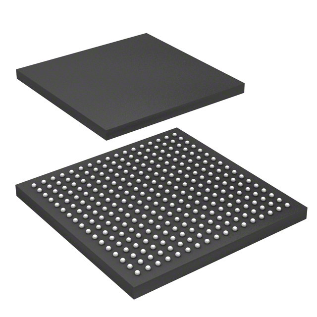


 工商网监
湘ICP备2023018690号
工商网监
湘ICP备2023018690号
